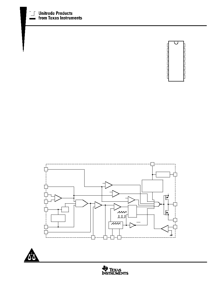
UCC2819, UCC3819
PROGRAMMABLE OUTPUT
POWER FACTOR PREREGULATOR
SLUS482A - APRIL 2001 ≠ REVISED JANUARY 2002
1
www.ti.com
D
Controls Boost Preregulator to Near-Unity
Power Factor
D
World Wide Line Operation
D
Over-Voltage Protection
D
Accurate Power Limiting
D
Average Current Mode Control
D
Improved Noise Immunity
D
Improved Feed-Forward Line Regulation
D
Leading Edge Modulation
D
150-
µ
A Typical Start-Up Current
D
Low-Power BiCMOS Operation
D
10.8-V to 17-V Operation
D
Programmable Output Voltage (Tracking
Boost Topology)
description
The UCC2819/UCC3819 provides all the functions necessary for active power factor corrected preregulators.
The controller achieves near unity power factor by shaping the ac-input line current waveform to correspond
to that of the ac-input line voltage. Average current mode control maintains stable, low distortion sinusoidal line
current.
Designed in Texas Instrument's BiCMOS process, the UCC3819 offers new features such as lower start-up
current, lower power dissipation, overvoltage protection, a shunt UVLO detect circuitry and a leading-edge
modulation technique to reduce ripple current in the bulk capacitor.
The UCC3819 allows the output voltage to be programmed by bringing out the error amplifier noninverting input.
Available in the 16-pin D, DW, N, and PW packages.
block diagram
UDG-01009
VREF
9
2
16
1
15
10
5
4
DRVOUT
GND
CAI
VCC
OVP/EN
VAOUT
1.9 V
PKLMT
7.5 V
REFERENCE
UVLO
16 V/10 V
10.5 V/10 V
VCC
3
OSCILLATOR
12
RT
14
CT
S
Q
R
PWM
LATCH
+
≠
PWM
CAOUT
+
≠
+
≠
+
≠
VOLTAGE
ERROR AMP
8.0 V
7
11
VSENSE
VFF
8
IAC
6
MOUT
MIRROR
2:1
X
2
+
≠
ENABLE
OVP
˜
X
X
MULT
OSC
CLK
CLK
CURRENT
AMP
+
≠
0.33 V
ZERO POWER
R
+
≠
13
VAI
(UCC2819)
(UCC3819)
Copyright
2002, Texas Instruments Incorporated
PRODUCTION DATA information is current as of publication date.
Products conform to specifications per the terms of Texas Instruments
standard warranty. Production processing does not necessarily include
testing of all parameters.
Please be aware that an important notice concerning availability, standard warranty, and use in critical applications of
Texas Instruments semiconductor products and disclaimers thereto appears at the end of this data sheet.
D, DW, N, and PW PACKAGES
(TOP VIEW)
1
2
3
4
5
6
7
8
16
15
14
13
12
11
10
9
GND
PKLMT
CAOUT
CAI
MOUT
IAC
VAOUT
VFF
DRVOUT
VCC
CT
VAI
RT
VSENSE
OVP/EN
VREF
UCC2819, UCC3819
PROGRAMMABLE OUTPUT
POWER FACTOR PREREGULATOR
SLUS482A - APRIL 2001 ≠ REVISED JANUARY 2002
2
www.ti.com
absolute maximum ratings over operating free-air temperature (unless otherwise noted)
Supply voltage, VCC
18 V
. . . . . . . . . . . . . . . . . . . . . . . . . . . . . . . . . . . . . . . . . . . . . . . . . . . . . . . . . . . . . . . . . . . . . . . .
Gate drive current, continuous
0.2 A
. . . . . . . . . . . . . . . . . . . . . . . . . . . . . . . . . . . . . . . . . . . . . . . . . . . . . . . . . . . . . .
Gate drive current
1.2 A
. . . . . . . . . . . . . . . . . . . . . . . . . . . . . . . . . . . . . . . . . . . . . . . . . . . . . . . . . . . . . . . . . . . . . . . . .
Input voltage, CAI, MOUT
8 V
. . . . . . . . . . . . . . . . . . . . . . . . . . . . . . . . . . . . . . . . . . . . . . . . . . . . . . . . . . . . . . . . . . . .
Input voltage, PKLMT
5 V
. . . . . . . . . . . . . . . . . . . . . . . . . . . . . . . . . . . . . . . . . . . . . . . . . . . . . . . . . . . . . . . . . . . . . . . .
Input voltage, VSENSE, OVP/EN, VAI
10 V
. . . . . . . . . . . . . . . . . . . . . . . . . . . . . . . . . . . . . . . . . . . . . . . . . . . . . . . . .
Input current, RT, IAC, PKLMT
10 mA
. . . . . . . . . . . . . . . . . . . . . . . . . . . . . . . . . . . . . . . . . . . . . . . . . . . . . . . . . . . . .
Maximum negative voltage, DRVOUT, PKLMT, MOUT
≠0.5 V
. . . . . . . . . . . . . . . . . . . . . . . . . . . . . . . . . . . . . . . .
Power dissipation
1 W
. . . . . . . . . . . . . . . . . . . . . . . . . . . . . . . . . . . . . . . . . . . . . . . . . . . . . . . . . . . . . . . . . . . . . . . . . . .
Stresses beyond those listed under "absolute maximum ratings" may cause permanent damage to the device. These are stress ratings only, and
functional operation of the device at these or any other conditions beyond those indicated under recommended operating conditions is not implied.
Exposure to absolute-maximum-rated conditions for extended periods may affect device reliability.
AVAILABLE OPTIONS
T
PACKAGE DEVICES
TJ
D PACKAGE
DW PACKAGE
N PACKAGE
PW PACKAGE
0
∞
C to 70
∞
C
UCC3819D
UCC3819DW
UCC3819N
UCC3819PW
≠40
∞
C to 85
∞
C
UCC2819D
UCC2819DW
UCC2819N
UCC2819PW
The D, DW, and PW packages are available taped and reeled. Add TR suffix to device type (e.g. UCC3819DTR) to
order quantities of 2500 devices per reel.
electrical characteristics
, T
A
= 0
∞
C to 70
∞
C for the UCC3819, ≠40
∞
C to 85
∞
C for the UCC2819, VCC = 12 V,
R
T
= 22 k
, C
T
= 270 pF, (unless otherwise noted)
supply current
PARAMETER
TEST CONDITIONS
MIN
TYP
MAX
UNITS
Supply current, off
VCC = (VCC turnon threshold ≠0.3 V)
150
300
µ
A
Supply current, on
VCC = 12 V,
No load on DRVOUT
2
4
6
mA
UVLO
PARAMETER
TEST CONDITIONS
MIN
TYP
MAX
UNITS
VCC turnon threshold
9.7
10.2
10.8
V
VCC turnoff threshold
9.4
9.7
V
UVLO hysteresis
0.3
0.5
V
voltage amplifier
PARAMETER
TEST CONDITIONS
MIN
TYP
MAX
UNITS
VIO
VAOUT = 2.75 V,
VCM = 3.75 V
≠15
15
mV
VAI bias current
VAOUT = 2.75 V,
VCM = 3.75 V
50
200
nA
VSENSE bias current
VSENSE = VREF,
VAOUT = 2.5 V
50
200
nA
CMRR
VCM = 1 V to 7.5 V
50
70
dB
Open loop gain
VAOUT = 2 V to 5 V
50
90
dB
High-level output voltage
IL = ≠150
µ
A
5.3
5.5
5.6
V
Low-level output voltage
IL = 150
µ
A
0
50
150
mV

UCC2819, UCC3819
PROGRAMMABLE OUTPUT
POWER FACTOR PREREGULATOR
SLUS482A - APRIL 2001 ≠ REVISED JANUARY 2002
3
www.ti.com
electrical characteristics
, T
A
= 0
∞
C to 70
∞
C for the UCC3819, ≠40
∞
C to 85
∞
C for the UCC2819, VCC = 12 V,
R
T
= 22 k
, C
T
= 270 pF, (unless otherwise noted)
over voltage protection and enable
PARAMETER
TEST CONDITIONS
MIN
TYP
MAX
UNITS
Over voltage reference
VREF
+0.48
VREF
+0.50
VREF
+0.52
V
Hysteresis
300
500
600
mV
Enable threshold
1.7
1.9
2.1
V
Enable hysteresis
0.1
0.2
0.3
V
current amplifier
PARAMETER
TEST CONDITIONS
MIN
TYP
MAX
UNITS
Input offset voltage
VCM = 0 V,
VCAOUT = 3 V
≠2
0
2
mV
Input bias current
VCM = 0 V,
VCAOUT = 3 V
≠50
≠100
nA
Input offset current
VCM = 0 V,
VCAOUT = 3 V
25
100
nA
Open loop gain
VCM = 0 V,
VCAOUT = 2 V to 5 V
90
dB
Common-mode rejection ratio
VCM = 0 V to 1.5 V,
VCAOUT = 3 V
60
80
dB
High-level output voltage
IL = ≠120
µ
A
5.6
6.5
6.8
V
Low-level output voltage
IL = 1 mA
0.1
0.2
0.5
V
Gain bandwidth product
See Note 1
2.5
MHz
voltage reference
PARAMETER
TEST CONDITIONS
MIN
TYP
MAX
UNITS
Input voltage, (UCC3819)
TA = 0
∞
C to 70
∞
C
7.387
7.5
7.613
V
Input voltage, (UCC2819)
TA = ≠40
∞
C to 85
∞
C
7.369
7.5
7.631
V
Load regulation
IREF = 1 mA to 2 mA
0
10
mV
Line regulation
VCC = 10.8 V to 15 V,
See Note 2
0
10
mV
Short-circuit current
VREF = 0 V
≠20
≠25
≠50
mA
oscillator
PARAMETER
TEST CONDITIONS
MIN
TYP
MAX
UNITS
Initial accuracy
TA = 25
∞
C
85
100
115
kHz
Voltage stability
VCC = 10.8 V to 15 V
≠1
1
%
Total variation
Line, temp,
See Note 1
80
120
kHz
Ramp peak voltage
4.5
5
5.5
V
Ramp amplitude voltage
(peak to peak)
3.5
4
4.5
V
NOTES: 1. Ensured by design, Not production tested.
2. Reference variation for VCC < 10.8 V is shown in Figure 2.
UCC2819, UCC3819
PROGRAMMABLE OUTPUT
POWER FACTOR PREREGULATOR
SLUS482A - APRIL 2001 ≠ REVISED JANUARY 2002
4
www.ti.com
electrical characteristics
, T
A
= 0
∞
C to 70
∞
C for the UCC3819, ≠40
∞
C to 85
∞
C for the UCC2819, VCC = 12 V,
R
T
= 22 k
, C
T
= 270 pF, (unless otherwise noted)
peak current limit
PARAMETER
TEST CONDITIONS
MIN
TYP
MAX
UNITS
PKLMT reference voltage
≠15
15
mV
PKLMT propagation delay
150
350
500
ns
multiplier
PARAMETER
TEST CONDITIONS
MIN
TYP
MAX
UNITS
IMOUT, high line, low power output
current, (0
∞
C to 85
∞
C)
IAC = 500
µ
A, VFF = 4.7 V,
VAOUT = 1.25 V
0
≠6
≠20
µ
A
IMOUT, high line, low power output
current, (≠40
∞
C to 85
∞
C)
IAC = 500
µ
A, VFF = 4.7 V,
VAOUT = 1.25 V
0
≠23
µ
A
IMOUT, high line, high power output
current
IAC = 500
µ
A, VFF = 4.7 V,
VAOUT = 5 V
≠70
≠90
≠105
µ
A
IMOUT, low line, low power output
current
IAC = 150
µ
A, VFF = 1.4 V,
VAOUT = 1.25 V
≠10
≠19
≠50
µ
A
IMOUT, low line, high power output
current
IAC = 150
µ
A, VFF = 1.4 V,
VAOUT = 5 V
≠268
≠300
≠346
µ
A
IMOUT, IAC limited
IAC = 150
µ
A, VFF = 1.3 V,
VAOUT = 5 V
≠250
≠300
≠400
µ
A
Gain constant (K)
IAC = 300
µ
A, VFF = 3 V,
VAOUT = 2.5 V
0.5
1
1.5
1/V
I
ero c rrent
IAC = 150
µ
A, VFF = 1.4 V,
VAOUT = 0.25 V
0
≠2
µ
A
IMOUT, zero current
IAC = 500
µ
A, VFF = 4.7 V,
VAOUT = 0.25 V
0
≠2
µ
A
IMOUT, zero current, (0
∞
C to 85
∞
C)
IAC = 500
µ
A, VFF = 4.7 V,
VAOUT = 0.5 V
0
≠3
µ
A
IMOUT, zero current, (≠40
∞
C to 85
∞
C)
IAC = 500
µ
A, VFF = 4.7 V,
VAOUT = 0.5 V
0
≠3.5
µ
A
Power limit (IMOUT x VFF)
IAC = 150
µ
A, VFF = 1.4 V,
VAOUT = 5 V
≠375
≠420
≠485
µ
W
feed-forward
PARAMETER
TEST CONDITIONS
MIN
TYP
MAX
UNITS
VFF output current
IAC = 300
µ
A
≠140
≠150
≠160
µ
A
gate driver
PARAMETER
TEST CONDITIONS
MIN
TYP
MAX
UNITS
Pullup resistance
IO = ≠100 mA to ≠200 mA
5
12
Pulldown resistance
IO = 100 mA
2
10
Output rise time
CL = 1 nF,
RL = 10
,
VDRVOUT = 0.7 V to 9 V
25
50
ns
Output fall time
CL = 1 nF,
RL = 10
,
VDRVOUT = 9 V to 0.7 V
10
50
ns
Maximum duty cycle
93
95
100
%
Minimum controlled duty cycle
At 100 kHz
2
%
zero power
PARAMETER
TEST CONDITIONS
MIN
TYP
MAX
UNITS
Zero power comparator threshold
Measured on VAOUT
0.20
0.33
0.50
V

UCC2819, UCC3819
PROGRAMMABLE OUTPUT
POWER FACTOR PREREGULATOR
SLUS482A - APRIL 2001 ≠ REVISED JANUARY 2002
5
www.ti.com
pin descriptions
CAI: (current amplifier noninverting input) Place a resistor between this pin and the GND side of current-sense
resistor. This input and the inverting input (MOUT) remain functional down to and below GND.
CAOUT: (current amplifier output) This is the output of a wide bandwidth operational amplifier that senses line
current and commands the PFC pulse-width modulator (PWM) to force the correct duty cycle. Compensation
components are placed between CAOUT and MOUT.
CT: (oscillator timing capacitor) A capacitor from CT to GND sets the PWM oscillator frequency according to:
f
[
0.6
RT
CT
The lead from the oscillator timing capacitor to GND should be as short and direct as possible.
DRVOUT: (gate drive) The output drive for the boost switch is a totem-pole MOSFET gate driver on DRVOUT.
Use a series gate resistor to prevent interaction between the gate impedance and the output driver that might
cause the DRVOUT to overshoot excessively. See characteristic curve (Figure 13) to determine minimum
required gate resister value. Some overshoot of the DRVOUT output is always expected when driving a
capacitive load.
GND: (ground) All voltages measured with respect to ground. VCC and REF should be bypassed directly to
GND with a 0.1-
µ
F or larger ceramic capacitor.
IAC: (current proportional to input voltage) This input to the analog multiplier is a current proportional to
instantaneous line voltage. The multiplier is tailored for very low distortion from this current input (I
IAC
) to
multiplier output. The recommended maximum I
IAC
is 500
µ
A.
MOUT: (multiplier output and current amplifier inverting input) The output of the analog multiplier and the
inverting input of the current amplifier are connected together at MOUT. As the multiplier output is a current, this
is a high-impedance input so the amplifier can be configured as a differential amplifier. This configuration
improves noise immunity and allows for the leading-edge modulation operation. The multiplier output current
is limited to 2
I
IAC
. The multiplier output current is given by the equation:
I
MOUT
+
I
IAC
(V
VAOUT
*
1)
V
VFF
2
K
where K
+
1
V
is the multiplier gain constant.
OVP/EN: (over-voltage/enable) A window comparator input that disables the output driver if the boost output
voltage is a programmed level above the nominal or disables both the PFC output driver and resets SS if pulled
below 1.9 V (typ).
PKLMT: (PFC peak current limit) The threshold for peak limit is 0 V. Use a resistor divider from the negative side
of the current sense resistor to VREF to level shift this signal to a voltage level defined by the value of the sense
resistor and the peak current limit. Peak current limit is reached when PKLMT voltage falls below 0 V.
RT: (oscillator charging current) A resistor from RT to GND is used to program oscillator charging current. A
resistor between 10 k
and 100 k
is recommended. Nominal voltage on this pin is 3 V.

UCC2819, UCC3819
PROGRAMMABLE OUTPUT
POWER FACTOR PREREGULATOR
SLUS482A - APRIL 2001 ≠ REVISED JANUARY 2002
6
www.ti.com
pin descriptions (continued)
VAI: (voltage amplifier non-inverting input) This input can be tied to the VREF or any other voltage reference
(
7.5 V) to set the boost regulator output voltage.
VAOUT: (voltage amplifier output) This is the output of the operational amplifier that regulates output voltage.
The voltage amplifier output is internally limited to approximately 5.5 V to prevent overshoot.
VCC: (positive supply voltage) Connect to a stable source of at least 20 mA between 10 V and 17 V for normal
operation. Bypass VCC directly to GND to absorb supply current spikes required to charge external MOSFET
gate capacitances. To prevent inadequate gate drive signals, the output devices are inhibited unless V
VCC
exceeds the upper under-voltage lockout voltage threshold and remains above the lower threshold.
VFF: (feed-forward voltage) The RMS voltage signal generated at this pin by mirroring 1/2 of the I
IAC
into a single
pole external filter. At low line, the VFF roll should be 14 V.
VSENSE: (voltage amplifier inverting input) This is normally connected to a compensation network and to the
boost converter output through a divider network.
VREF: (voltage reference output) VREF is the output of an accurate 7.5-V voltage reference. This output is
capable of delivering 20 mA to peripheral circuitry and is internally short-circuit current limited. VREF is disabled
and remains at 0 V when V
VCC
is below the UVLO threshold. Bypass VREF to GND with a 0.1-
µ
F or larger
ceramic capacitor for best stability. Please refer to Figures 8 and 9 for VREF line and load regulation
characteristics.
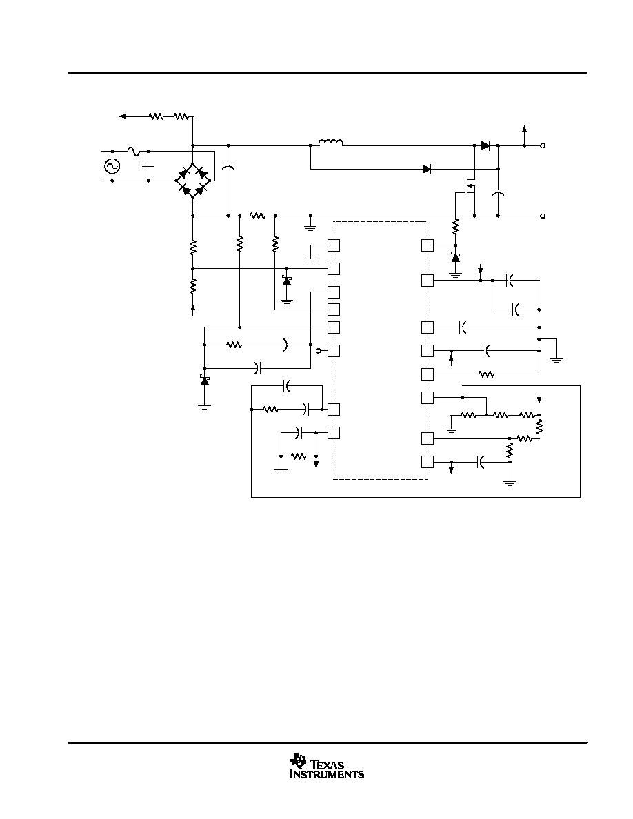
APPLICATION INFORMATION
The UCC3819 is based on the UCC3818 PFC preregulator. For a more detailed application information for this
part, please refer to the UCC3818 datasheet product folder.
The main difference between the UCC3818 and the UCC3819 is that the non-inverting input of the voltage error
amplifier is made available to the user through an external pin (VAI) in the UCC3819. The SS pin and function
were eliminated to accommodate this change.
The benefit of VAI pin is that it can be used to dynamically change the PFC output voltage based on the line
voltage (RMS) level or other conditions. Figure 1 shows one suggested implementation of the tracking boost
PFC converter as this approach is sometimes referred to. The VAI pin is tied to the VFF pin and hence output
voltage scales up with the line voltage. The benefit of this approach is that at lower line voltages the output
voltage is lower and that leads to smaller boost inductor value, lower MOSFET conduction losses and reduced
component stresses. In order for this feature to work, the downstream converter has to operate over a wider
input range.
UCC2819, UCC3819
PROGRAMMABLE OUTPUT
POWER FACTOR PREREGULATOR
SLUS482A - APRIL 2001 ≠ REVISED JANUARY 2002
7
www.ti.com
APPLICATION INFORMATION
UDG≠01008
1
11
7
16
GND
DRVOUT
R17
15
C3
C2
14
C1
13
C4
12
R1
R3
R2
R4
R5
C5
9
4
10
VREF
VCC
CT
VAI
RT
VSENSE
OVP/EN
VREF
VAOUT
3
8
2
VFF
C6
C7
R7
6
5
R9
C8
R8
D6
R10
D5
R11
R12
R14
C13
C14
R13
IAC
D2
D1
C12
VOUT
+
≠
PKLIMIT
CAOUT
CAI
MOUT
IAC
VO
UCC3819
VLINE
VREF
C9
R6
D3
Q1
F1
VO
D4
R19
R20
R21
AC2
AC1
C15
VFF
VCC (FROM BIAS SUPPLY)
Figure 1. Suggested Implementation of UCC3819 in a Tracking Boost PFC Preregulator

UCC2819, UCC3819
PROGRAMMABLE OUTPUT
POWER FACTOR PREREGULATOR
SLUS482A - APRIL 2001 ≠ REVISED JANUARY 2002
8
www.ti.com
APPLICATION INFORMATION
Figure 2
14
12
10
7.45
7.50
7.55
7.60
7.40
VCC ≠ Supply Voltage ≠ V
13
11
9
VREF
≠
Reference V
o
ltage
≠
V
REFERENCE VOLTAGE
vs
SUPPLY VOLTAGE
Figure 3
REFERENCE VOLTAGE
vs
REFERENCE CURRENT
0
5
10
15
20
25
7.495
7.500
7.505
7.510
7.490
VREF
≠
Reference V
o
ltage
≠
V
IVREF ≠ Reference Current ≠ mA
Figure 4
MULTIPLIER OUTPUT CURRENT
vs
VOLTAGE ERROR AMPLIFIER OUTPUT
0.0
1.0
2.0
3.0
4.0
5.0
50
200
250
350
0
100
300
150
IAC = 150
µ
A
IAC = 300
µ
A
IAC = 500
µ
A
I MO
UT
-
Multiplier Output Current
≠
µ
A
VAOUT ≠ Voltage
Error Amplifier
Output ≠ V
Figure 5
MULTIPLIER GAIN
vs
VOLTAGE ERROR AMPLIFIER OUTPUT
1.0
2.0
3.0
4.0
5.0
0.7
1.1
1.3
1.5
0.5
0.9
IAC = 300
µ
A
IAC = 500
µ
A
IAC = 150
µ
A
Multiplier
Gain
≠
K
VAOUT ≠ Voltage
Error Amplifier
Output ≠ V
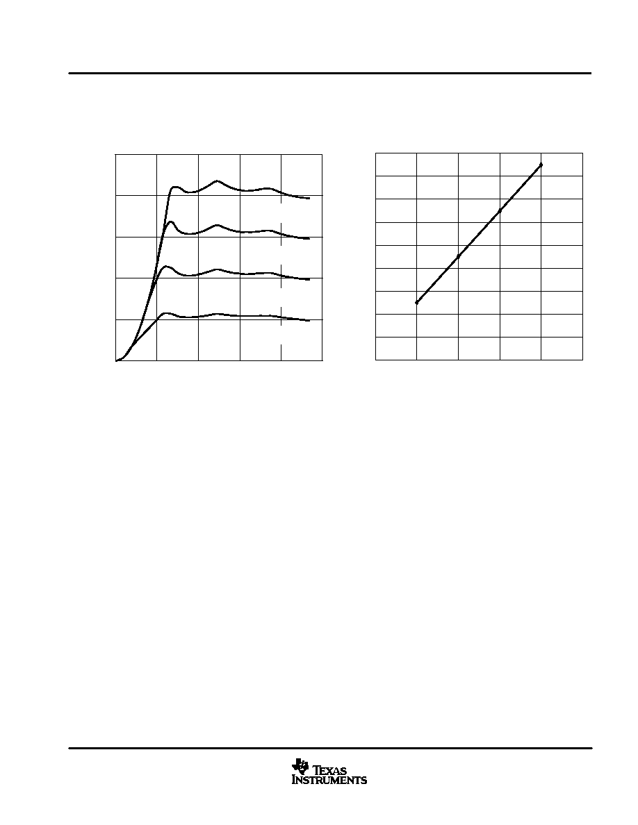
UCC2819, UCC3819
PROGRAMMABLE OUTPUT
POWER FACTOR PREREGULATOR
SLUS482A - APRIL 2001 ≠ REVISED JANUARY 2002
9
www.ti.com
APPLICATION INFORMATION
Figure 6
VFF ≠ Feedforward Voltage ≠ V
1.0
2.0
3.0
4.0
5.0
100
300
400
500
0
200
VAOUT = 3 V
VAOUT = 2 V
VAOUT = 4 V
VAOUT = 5 V
(VFF
◊
I
MO
UT
)
≠
µ
W
MULTIPLIER CONSTANT POWER PERFORMANCE
0.0
Figure 7
10
12
14
16
20
10
14
15
17
8
12
18
9
11
13
16
RECOMMENDED MINIMUM GATE RESISTANCE
vs
SUPPLY VOLTAGE
R
GA
TE
-
Recommended
Minimum Gate Resistance
≠
VCC ≠ Supply Voltage ≠ V

IMPORTANT NOTICE
Texas Instruments Incorporated and its subsidiaries (TI) reserve the right to make corrections, modifications,
enhancements, improvements, and other changes to its products and services at any time and to discontinue
any product or service without notice. Customers should obtain the latest relevant information before placing
orders and should verify that such information is current and complete. All products are sold subject to TI's terms
and conditions of sale supplied at the time of order acknowledgment.
TI warrants performance of its hardware products to the specifications applicable at the time of sale in
accordance with TI's standard warranty. Testing and other quality control techniques are used to the extent TI
deems necessary to support this warranty. Except where mandated by government requirements, testing of all
parameters of each product is not necessarily performed.
TI assumes no liability for applications assistance or customer product design. Customers are responsible for
their products and applications using TI components. To minimize the risks associated with customer products
and applications, customers should provide adequate design and operating safeguards.
TI does not warrant or represent that any license, either express or implied, is granted under any TI patent right,
copyright, mask work right, or other TI intellectual property right relating to any combination, machine, or process
in which TI products or services are used. Information published by TI regarding third≠party products or services
does not constitute a license from TI to use such products or services or a warranty or endorsement thereof.
Use of such information may require a license from a third party under the patents or other intellectual property
of the third party, or a license from TI under the patents or other intellectual property of TI.
Reproduction of information in TI data books or data sheets is permissible only if reproduction is without
alteration and is accompanied by all associated warranties, conditions, limitations, and notices. Reproduction
of this information with alteration is an unfair and deceptive business practice. TI is not responsible or liable for
such altered documentation.
Resale of TI products or services with statements different from or beyond the parameters stated by TI for that
product or service voids all express and any implied warranties for the associated TI product or service and
is an unfair and deceptive business practice. TI is not responsible or liable for any such statements.
Mailing Address:
Texas Instruments
Post Office Box 655303
Dallas, Texas 75265
Copyright
2001, Texas Instruments Incorporated