
UCC281-3/-5/-ADJ
UCC381-3/-5/-ADJ
SLUS214B -JANUARY 2001
FEATURES
∑
Precision Positive Linear Voltage
Regulation
∑
0.5V Dropout at 1A
∑
Guaranteed Reverse Input/ Output
Voltage Isolation with Low Leakage
∑
Low Quiescent Current Irrespective of
Load
∑
Adjustable Output Voltage Version
∑
Fixed Versions for 3.3V and 5V
Outputs
∑
Logic Shutdown Capability
∑
Short Circuit Power Limit of
3%
∑
V
IN
∑
Current Limit
∑
Remote Load Voltage for Accurate
Load Regulation
DESCRIPTION
The UCC381-3/-5/-ADJ family of positive linear series pass regulators is
tailored for low drop out applications where low quiescent power is impor-
tant. Fabricated with a BiCMOS technology ideally suited for low input to
output differential applications, the UCC381 will pass 1A while requiring
only 0.5V of input voltage headroom. Dropout voltage decreases linearly
with output current, so that dropout at 200mA is less than 100mV. Quies-
cent current is always less than 650
µ
A. To prevent reverse current conduc-
tion, on-chip circuitry limits the minimum forward voltage to typically 50mV.
Once the forward voltage limit is reached, the input-output differential volt-
age is maintained as the input voltage drops until undervoltage lockout dis-
ables the regulator.
UCC381-3 and UCC381-5 versions have on-chip resistor networks preset
to regulate either 3.3V or 5.0V, respectively. Furthermore, remote sensing
of the load voltage is possible by connecting the VOUTS pin directly at the
load. The output voltage is then regulated to 1.5% at room temperature and
better than 2.5% over temperature. The UCC381-ADJ version has a regu-
lated output voltage programmed by an external user-definable resistor ra-
tio.
(continued)
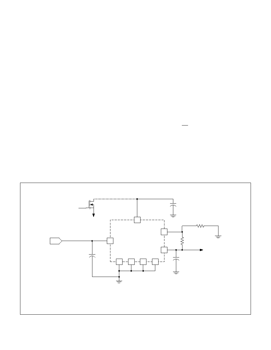
Low Dropout 1 Ampere Linear Regulator Family
1
VOUT
2
GND
7
GND
R2
R1
+
≠
V
PUMP
UVLO
+
≠
8
1.3/2.1A
CURRENT
REFERENCE
VIN
UCC381-ADJ
UCC381-3
UCC381-5
R2
R1
0
OPEN
82k
50k
150k
50k
4
3
GND
6
GND
1.25V
VOUTS
VOLTAGE
AMPLIFIER
CURRENT
LIMIT
THERMAL
SHUTDOWN
REVERSE VOLTAGE
SENSE
3% DUTY CYCLE
CURRENT LIMIT TIMER
5
0.65V
CT*
SHUTDOWN FOR FIXED VERSIONS
*ADJ
VERSION
ONLY
BLOCK DIAGRAM
UDG-98112
2
UCC281-3/-5/-ADJ
UCC381-3/-5/-ADJ
ABSOLUTE MAXIMUM RATINGS
VIN. . . . . . . . . . . . . . . . . . . . . . . . . . . . . . . . . . . . . . . . . . . . . 9V
CT . . . . . . . . . . . . . . . . . . . . . . . . . . . . . . . . . . . . . . .
-
0.3 to 3V
Storage Temperature . . . . . . . . . . . . . . . . . . .
-
65
∞
C to +150
∞
C
Junction Temperature . . . . . . . . . . . . . . . . . . .
-
55
∞
C to +150
∞
C
Lead Temperature (Soldering, 10 sec.) . . . . . . . . . . . . . +300
∞
C
Currents are positive into, negative out of the specified terminal.
Consult Packaging Section of Databook for thermal limitations
and considerations of packages. All voltages are referenced to
GND.
ELECTRICAL CHARACTERISTICS:
Unless otherwise stated, these specifications hold for T
A
= 0
∞
C to 70
∞
C for the
UCC381-X series and
-
40
∞
C to +85
∞
C for the UCC283-X series, V
IN
= V
OUT
+ 1.5V, I
OUT
= 0mA, C
OUT
= 2.2
µ
F. C
T
= 1500pF for
the UCC381-ADJ version and V
OUT
set to 5V. T
J
= T
A
.
PARAMETER
TEST CONDITIONS
MIN
TYP
MAX
UNITS
UCC381-5 Fixed 5V, 1A Family
Output Voltage
T
J
= 25∞C
4.925
5
5.075
V
Over Temperature
4.875
5.125
V
Line Regulation
V
IN
= 5.15V to 9V
1
3
mV
Load Regulation
I
OUT
= 0mA to 1A
2
5
mV
Drop Out Voltage, V
IN
≠ V
OUT
I
OUT
= 1A, V
OUT
= 4.85V, TA < 85∞C
0.5
0.6
V
I
OUT
= 200mA, V
OUT
= 4.85V, TA < 85∞C
100
200
mV
Peak Current Limit
V
OUT
= 0V
2
3.5
A
Overcurrent Threshold
1
1.8
A
Current Limit Duty Cycle
V
OUT
= 0V
3
5
%
Overcurrent Time Out, T
ON
V
OUT
= 0V
400
750
1600
µ
s
Quiescent Current
400
650
µ
A
Quiescent Current in Shutdown
V
IN
= 9V
10
25
µ
A
Shutdown Threshold
At C
T
Input
0.25
0.65
V
Reverse Leakage Current
1V < V
IN
< V
OUT
, V
OUT
< 5.1V, at V
OUT
75
µ
A
UVLO Threshold
V
IN
where V
OUT
passes current
2.5
2.8
3.0
V
Short circuit current is internally limited. The device re-
sponds to a sustained overcurrent condition by turning
off after a T
ON
delay. The device then stays off for a pe-
riod, T
OFF
, that is 32 times the T
ON
delay. The device
then begins pulsing on and off at the T
ON
/(T
ON
+T
OFF
)
duty cycle of 3%. This drastically reduces the power dis-
sipation during short circuit such that heat sinking, if at all
required, must only accommodate normal operation. On
the fixed output versions of the device T
ON
is fixed at
400
µ
s
-
a guaranteed minimum. On the adjustable ver-
sion an external capacitor sets the on time. The off time
is always 32 times T
ON
.
The UCC381 can be shutdown to 25
µ
A (max) by pulling
the CT pin low.
Internal power dissipation is further controlled with ther-
mal overload protection circuitry. Thermal shutdown oc-
curs if the junction temperature exceeds 165
∞
C. The chip
will remain off until the temperature has dropped 20
∞
C.
The UCC281 series is specified for operation over the in-
dustrial range of
-
40
∞
C to +85
∞
C, and the UCC381 se-
ries is specified from 0
∞
C to +70
∞
C. These devices are
available in the 8 pin DP surface mount power package.
For other packaging options consult the factory.
DESCRIPTION (cont.)
1
2
3
4
8
7
6
5
GND
VOUT
VOUTS
GND
GND
VIN
CT*
GND
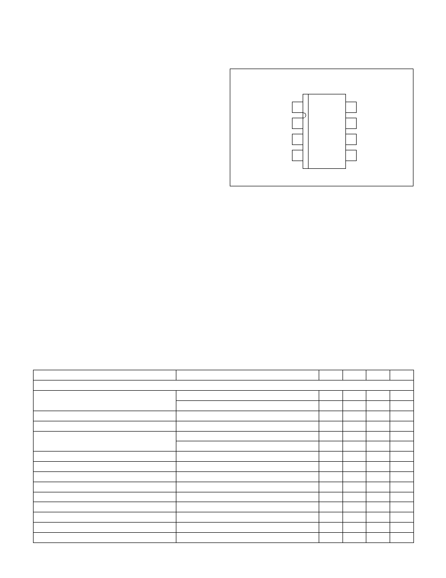
CONNECTION DIAGRAMS
SOIC-8 (Top View)
DP Package
* ADJ version only
3
UCC281-3/-5/-ADJ
UCC381-3/-5/-ADJ
ELECTRICAL CHARACTERISTICS:
Unless otherwise stated, these specifications hold for T
A
= 0
∞
C to 70
∞
C for the
UCC381-X series and
-
40
∞
C to +85
∞
C for the UCC283-X series, V
IN
= V
OUT
+ 1.5V, I
OUT
= 0mA, C
OUT
= 2.2
µ
F. C
T
= 1500pF for
the UCC381-ADJ version and V
OUT
set to 5V. T
J
= T
A
.
PARAMETER
TEST CONDITIONS
MIN
TYP
MAX
UNITS
UCC381-3 Fixed 3.3V, 1A Family
Output Voltage
T
J
= 25∞C
3.25
3.3
3.35
V
Over Temperature
3.22
3.38
V
Line Regulation
V
IN
= 3.45V to 9V
1
3
mV
Load Regulation
I
OUT
= 0mA to 1A
2
5
mV
Dropout Voltage, V
IN
- V
OUT
I
OUT
= 1A, V
OUT
= 3.15V, T
A
< 85∞C
0.6
0.8
V
I
OUT
= 200mA, V
OUT
= 3.15V, T
A
< 85∞C
100
200
mV
Peak Current Limit
V
OUT
= 0V
2
3.5
A
Overcurrent Threshold
1
1.8
A
Current Limit Duty Cycle
V
OUT
= 0V
3
5
%
Overcurrent Time Out, T
ON
V
OUT
= 0V
400
750
1600
µ
s
Quiescent Current
400
650
µ
A
Quiescent Current in Shutdown
V
IN
= 9V
10
25
µ
A
Shutdown Threshold
At C
T
Input
0.25
0.65
V
Reverse Leakage Current
1V < V
IN
< V
OUT
, V
OUT
< 3.35V, at V
OUT
75
µ
A
UVLO Threshold
V
IN
where V
OUT
passes current
2.5
2.8
3.0
V
UCC381-ADJ Adjustable Output, 1A Family
Regulating Voltage at ADJ Input
T
J
= 25∞C
1.23
1.25
1.27
V
Over Temperature
1.22
1.28
V
Line Regulation, at ADJ Input
V
IN
= V
OUT
+ 150mV to 9V
1
3
mV
Load Regulation, at ADJ Input
I
OUT
= 0mA to 1A
2
5
mV
Dropout Voltage, V
IN
- V
OUT
I
OUT
= 1A, V
OUT
= 4.85V
0.5
0.6
V
I
OUT
= 200mA, V
OUT
= 4.85V
100
200
mV
Peak Current Limit
V
OUT
= 0V
2
3.5
A
Overcurrent Threshold
1
1.8
A
Current Limit Duty Cycle
V
OUT
= 0V
3
5
%
Overcurrent Time Out, T
ON
V
OUT
= 0V, C
T
= 1500pF
400
1000
1600
µ
s
Quiescent Current
400
650
µ
A
Quiescent Current in Shutdown
V
IN
= 9V
10
25
µ
A
Shutdown Threshold
At C
T
Input
0.25
0.65
V
Reverse Leakage Current
1V < V
IN
< V
OUT
, V
OUT
< 9V, at V
OUT
100
µ
A
Bias Current at ADJ Input
100
250
nA
UVLO Threshold
V
IN
where V
OUT
passes current
2.5
2.8
3.0
V
4
UCC281-3/-5/-ADJ
UCC381-3/-5/-ADJ
PIN DESCRIPTIONS
CT: For UCC381-3 and UCC381-5 versions, this is the
shutdown pin which, when pulled low, turns off the regu-
lator output and puts the device in a low current state.
For the UCC381-ADJ version, a capacitor is required be-
tween the CT pin and GND to set the T
ON
time during
overcurrent according to the following (typical) equation:
T
C
ON
CT
=
∑
660 000
,
GND: All voltages are measured with respect to this pin.
This is the low noise ground reference input for regula-
tion. The output decoupling capacitor should be tied to
PIN 7.
VIN: Positive supply input for the regulator. Bypass this
pin to GND with at least 1
µ
F of low ESR, ESL capaci-
tance if the source is located further than 1 inch from the
device.
VOUT: Output for regulator. The regulator does not re-
quire a minimum output capacitor for stability. Choose
the appropriate size capacitor for the application with re-
spect to the required transient loading. For example, if
the load is very dynamic, a large capacitor will smooth
out the response to load steps.
VOUTS: Feedback for regulator sensing of the output
voltage. For loads which are a considerable resistive dis-
tance from the VOUT pin, the VOUTS pin can be used to
move the resistance into the control loop of the regulator,
thereby effectively canceling the IR drop associated with
the load path. For local regulation, merely connect this
pin directly to the VOUT pin. For the UCC381-ADJ ver-
sion, the output voltage can be set by two external resi-
tors according to the following relationship:
V
R
R
OUT
=
∑ +
1 25
1
2
1
.
where R1 is a resistor connected between VOUT and
VOUTS and R2 is a resistor connected between VOUTS
and GND.
7
6
3
2
8
5
4
1
1.0
µ
F
R
1
NOTE 1
R
2
NOTE 1
C
T
NOTE 2
SHUTDOWN
V
IN
CT
VIN
GND
GND
GND
GND
VOUTS
VOUT
OUTPUT
C
OUT
UCC381
TYPICAL APPLICATION CIRCUIT
Note 1: R1 and R2 for adjustable version only. For 3.3V and 5V versions connect VOUT to VOUTS. See Pin Descriptions.
Note 2: C
T
timing capacitor is for adjustable version only. For 3.3V and 5V versions, the CT pin is used to enable or shutdown
the part. See Pin Descriptions.
UDG-98148
5
UCC281-3/-5/-ADJ
UCC381-3/-5/-ADJ
Overview
The UCC381 family of low dropout linear (LDO) regula-
tors provide a regulated output voltage for applications
with up to 1A of load current. The regulator features a
low dropout voltage and short circuit protection, making
their use ideal for demanding high current applications
requiring fault tolerance.
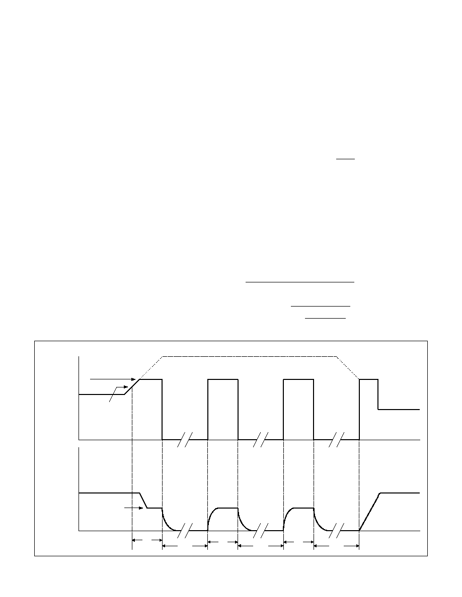
Short Circuit Protection
The UCC381 provides unique short circuit protection
circuitry that reduces power dissipation during a fault.
When an overload situation is detected, the device en-
ters a pulsed mode of operation at 3% duty cycle re-
ducing the heat sink requirements during a fault. The
UCC381 has two current thresholds that determine its
behavior during a fault as shown in Fig. 1.
When the regulator current exceeds the Overcurrent
Threshold for a period longer than the T
ON
, the
UCC381 shuts off for a period (T
OFF
) which is 32 times
T
ON
. If the short circuit current exceeds the Peak Cur-
rent Limit, the regulator limits the current to peak cur-
rent limit during the T
ON
period. The peak current limit
is nominally 1 Amp greater than the overcurrent thresh-
old. The regulator will continue in pulsed mode until the
fault is cleared as illustrated in Fig. 1.
A capacitive load on the regulator's output will appear as a
short circuit during start-up. If the capacitance is too large,
the output voltage will not come into regulation during the
initial T
ON
period and the UCC381 will enter pulsed mode
operation. The peak current limit, T
ON
period, and load
characteristics determine the maximum value of output ca-
pacitor that can be charged. For a constant current load
the maximum output capacitance is given as follows:
(
)
(
)
C
I
I
T
V
Farads
OUT
CL
LOAD
ON
OUT
max
=
-
∑
(1)
For worst case calculations the minimum values of on time
(T
ON
) and peak current limit (I
CL
) should be used. The ad-
justable version allows the T
ON
time to be adjusted with a
capacitor on the CT pin:
( )
(
)
(
)
T
C
Farads
ON adj
µ
µ
sec
,
=
∑
660 000
(2)
For a resistive load (R
LOAD
) the maximum output capacitor
can be estimated from:
(
)
C
T
R
n
V
I
R
OUT
ON
LOAD
OUT
CL
LOAD
max
=
∑
-
∑
l
1
1
Farads
(3)
APPLICATION INFORMATION
32T
ON
T
ON
T
ON
T
ON
32T
ON
32T
ON
V
O
(nom)
OUTPUT
VOLTAGE
I
O
(nom)
OUTPUT
CURRENT
R
OL
I
CL
PEAK CURRENT
LIMIT
OVERCURRENT
THRESHOLD
OVERLOAD
Figure 1. UCC381 short circuit timing.
UDG-98150
6
UCC281-3/-5/-ADJ
UCC381-3/-5/-ADJ
Dropout Performance
Referring to the Block Diagram, the dropout voltage of
the UCC381 is equal to the minimum voltage drop (V
IN
to
V
OUT
) across the N-Channel MOSFET. The dropout volt-
age is dependent on operating conditions such as load
current, input and load voltages, as well as temperature.
The UCC381 achieves a low Rds
(ON)
through the use of
an internal charge-pump (V
PUMP
) that drives the MOS-
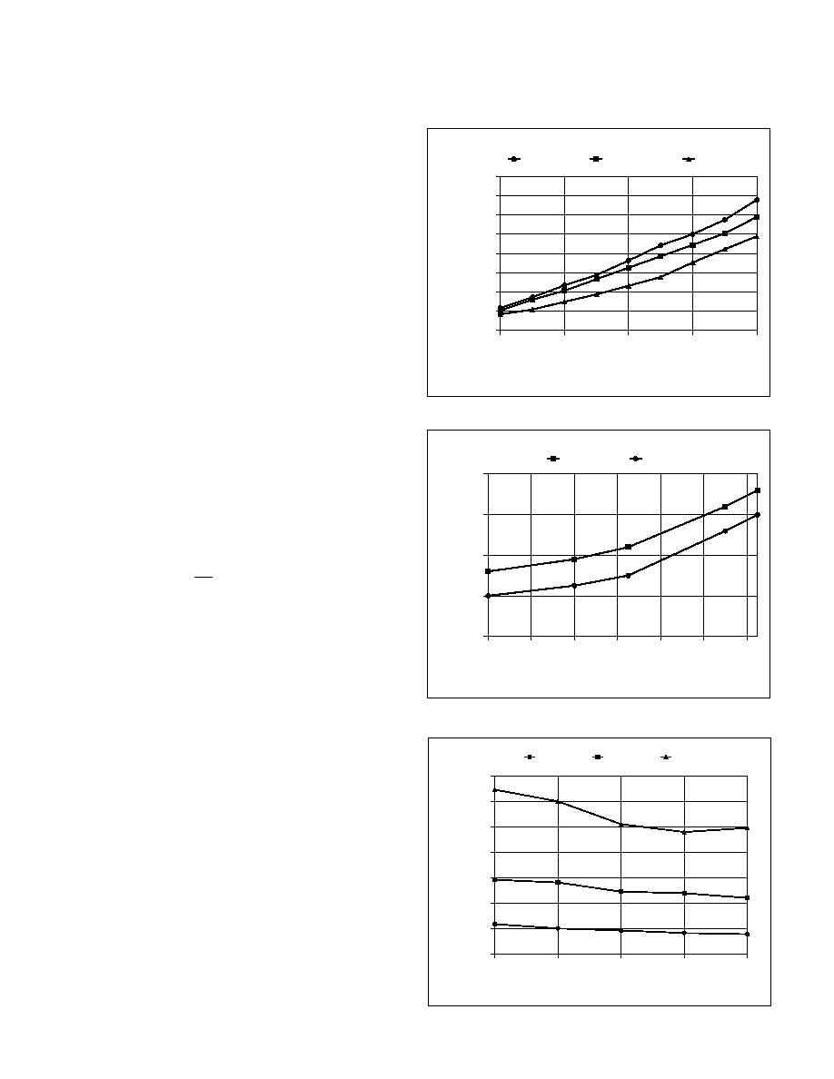
FET gate. Fig. 2 depicts typical dropout voltages versus
load current for the 3.3V and 5V versions of the part, as
well as the adjustable version programmed to 3.0V.
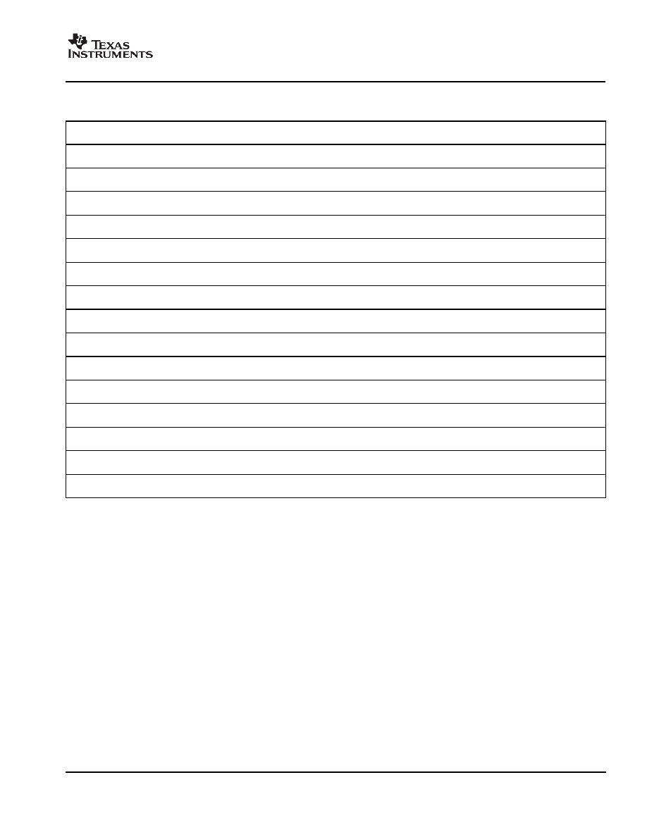
Fig. 3 depicts the typical dropout performance of the ad-
justable version with various output voltages and load
currents.
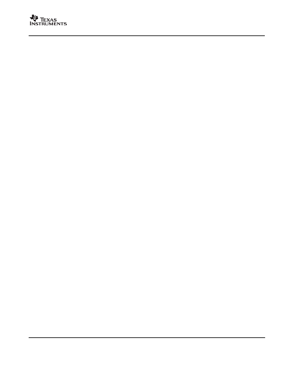
Operating temperatures effect the RDS(ON) and dropout
voltage of the UCC381. Fig. 4 graphs the typical dropout
for the 3.3V and 5V versions with a 3A load over tem-
perature.
Voltage Programming
Referring to the Typical Application Circuit, the output
voltage for the adjustable version is externally pro-
grammed through a resistive divider at the VOUTS pin as
shown.
V
R
R
Volts
OUT
=
∑ +
1 25
1
2
1
.
(4)
For the fixed Voltage versions the resistive divider is in-
ternally set, and the VOUTS pin should be connected to
the VOUT pin. The maximum programmed output volt-
age for the adjustable part is constrained by the 9V ab-
solute rating of the IC (including the charge pump
voltage) and its ability to enhance the N-Channel MOS-
FET. Unless the load current is well below the 1A rating
of the device, output voltages above 7V are not recom-
mended.
The minimum output voltage can be pro-
grammed down to 1.25V, however, the input voltage
must always be greater than the UVLO of the part.
Shutdown Feature
All versions include a shutdown feature, limiting quies-
cent current to 25
µ
A typical. The UCC381 is shut down
by pulling the CT pin to below 0.25V. As shown in the
applications circuit, a small logic level MOSFET or BJT
transistor connected to the CT pin can be driven with a
digital signal, putting the device in shutdown. If the CT
pin is not pulled low, the IC will internally pull up on the
pin, enabling the regulator. The CT pin should not be
forced high, as this will interfere with the short circuit pro-
tection feature. Selection of the timing capacitor for the
adjustable version is explained in the
Short Circuit Pro-
tection section.
APPLICATION INFORMATION (cont.)
0
0.1
0.2
0.3
0.4
0.5
0.6
0.7
3
3.5
4
4.5
5
V
OUT
(V)
V
IN
-V
OUT
(V
)
Iout = 0.2A
Iout = 0.5A
Iout = 1.0A
Figure 3. Typical dropout voltate vs. I
OUT
and V
OUT.
0
0.1
0.2
0.3
0.4
0.5
0.6
0.7
0.8
0.2
0.4
0.6
0.8
1
I
OUT
(A)
V
OUT
-V
IN
(V
)
Vout = 3V
Vout = 3.3V
Vout = 5V
Figure 2. Typical dropout vs. load current.
0.4
0.5
0.6
0.7
0.8
-40
-20
0
20
40
60
80
TEMPERATURE (∞C)
V
IN
-V
OUT
(V
)
DROP (3V)
DROP (5V)
Figure 4. Typical dropout vs. temperature (1A load).

7
UCC281-3/-5/-ADJ
UCC381-3/-5/-ADJ
UNITRODE CORPORATION
7 CONTINENTAL BLVD. ∑ MERRIMACK, NH 03054
TEL. (603) 424-2410 ∑ FAX (603) 424-3460
Thermal Design
The Packing Information section of the data book con-
tains reference material for the thermal ratings of various
packages. The section also includes an excellent article
Thermal Characteristics of Surface Mount Packages, that
is the basis of the following discussion.
Thermal design for the UCC381 includes two modes of
operation, normal and pulsed mode. In normal operation,
the linear regulator and heat sink must dissipate power
equal to the maximum forward voltage drop multiplied by
the maximum load current. Assuming a constant current
load, the expected heat rise at the regulator's junction
can be calculated as follows:
(
)
T
P
jc
ca
C
RISE
DISS
=
∑
+
∞
(5)
Where theta is thermal resistance and P
DISS
is the power
dissipated. The thermal resistance of both the SOIC-8
DP package (junction to case) is 22 degrees Celsius per
Watt. In order to prevent the regulator from going into
thermal shutdown, the case to ambient theta must keep
the junction temperature below 150C. If the LDO is
mounted on a 5 square inch pad of 1 ounce copper, for
example, the thermal resistance from junction to ambient
becomes 40-70 degrees Celsius per Watt. If a lower ther-
mal resistance is required by the application, the device
heat sinking would need to be improved.
When the UCC381 regulator is in pulsed mode, due to
an overload or short circuit in the application, the maxi-
mum
average power dissipation is calculated as follows:
(
)
(
)
P
V
V
I
T
T
Watts
PULSE avg
IN
OUT
CL
ON
ON
=
-
∑
∑
∑
33
(6)
As seen in equation 6, the average power during a fault
is reduced dramatically by the duty cycle, allowing the
heat sink to be sized for normal operation. Although the
peak power in the regulator during the T
ON
period can be
significant, the thermal mass of the package will gener-
ally keep the junction temperature from rising unless the
T
ON
period is increased to tens of milliseconds.
Ripple Rejection
Even though the UCC381 linear regulators are not opti-
mized for fast transient applications (Refer to UC182
"Fast LDO Linear Regulator"), they do offer significant
power supply rejection at lower frequencies. Fig 5. de-
picts ripple rejection performance in a typical application.
The performance can be improved with additional filter-
ing.
APPLICATION INFORMATION (cont.)
0
10
20
30
40
50
60
70
80
90
1.0E+02
1.0E+03
1.0E+04
1.0E+05
FREQUENCY
RI
PPLE
R
EJ
ECTI
ON
(
db)
10uF,
I
OUT
= 100mA
1uF, I
OUT
= 100mA
1uF, I
OUT
= 1A
10uF, I
OUT
= 1A
Figure 5. Ripple rejection vs. frequency.
PACKAGING INFORMATION
Orderable Device
Status
(1)
Package
Type
Package
Drawing
Pins Package
Qty
Eco Plan
(2)
Lead/Ball Finish
MSL Peak Temp
(3)
UCC281DP-5
ACTIVE
SOIC
D
8
75
Green (RoHS &
no Sb/Br)
CU NIPDAU
Level-2-260C-1 YEAR
UCC281DP-ADJ
ACTIVE
SOIC
D
8
75
Green (RoHS &
no Sb/Br)
CU NIPDAU
Level-2-260C-1 YEAR
UCC281DPTR-5
ACTIVE
SOIC
D
8
2500 Green (RoHS &
no Sb/Br)
CU NIPDAU
Level-2-260C-1 YEAR
UCC281DPTR-5G4
ACTIVE
SOIC
D
8
2500 Green (RoHS &
no Sb/Br)
CU NIPDAU
Level-2-260C-1 YEAR
UCC281DPTR-ADJ
ACTIVE
SOIC
D
8
2500 Green (RoHS &
no Sb/Br)
CU NIPDAU
Level-2-260C-1 YEAR
UCC281DPTR-ADJG4
ACTIVE
SOIC
D
8
2500 Green (RoHS &
no Sb/Br)
CU NIPDAU
Level-2-260C-1 YEAR
UCC381DP-3
ACTIVE
SOIC
D
8
75
Green (RoHS &
no Sb/Br)
CU NIPDAU
Level-2-260C-1 YEAR
UCC381DP-5
ACTIVE
SOIC
D
8
75
Green (RoHS &
no Sb/Br)
CU NIPDAU
Level-2-260C-1 YEAR
UCC381DP-ADJ
ACTIVE
SOIC
D
8
75
Green (RoHS &
no Sb/Br)
CU NIPDAU
Level-2-260C-1 YEAR
UCC381DP-ADJG4
ACTIVE
SOIC
D
8
75
Green (RoHS &
no Sb/Br)
CU NIPDAU
Level-2-260C-1 YEAR
UCC381DPTR-3
ACTIVE
SOIC
D
8
2500 Green (RoHS &
no Sb/Br)
CU NIPDAU
Level-2-260C-1 YEAR
UCC381DPTR-3G4
ACTIVE
SOIC
D
8
2500 Green (RoHS &
no Sb/Br)
CU NIPDAU
Level-2-260C-1 YEAR
UCC381DPTR-5
ACTIVE
SOIC
D
8
2500 Green (RoHS &
no Sb/Br)
CU NIPDAU
Level-2-260C-1 YEAR
UCC381DPTR-ADJ
ACTIVE
SOIC
D
8
2500 Green (RoHS &
no Sb/Br)
CU NIPDAU
Level-2-260C-1 YEAR
UCC381DPTR-ADJG4
ACTIVE
SOIC
D
8
2500 Green (RoHS &
no Sb/Br)
CU NIPDAU
Level-2-260C-1 YEAR
(1)
The marketing status values are defined as follows:
ACTIVE: Product device recommended for new designs.
LIFEBUY: TI has announced that the device will be discontinued, and a lifetime-buy period is in effect.
NRND: Not recommended for new designs. Device is in production to support existing customers, but TI does not recommend using this part in
a new design.
PREVIEW: Device has been announced but is not in production. Samples may or may not be available.
OBSOLETE: TI has discontinued the production of the device.
(2)
Eco
Plan
-
The
planned
eco-friendly
classification:
Pb-Free
(RoHS)
or
Green
(RoHS
&
no
Sb/Br)
-
please
check
http://www.ti.com/productcontent
for the latest availability information and additional product content details.
TBD: The Pb-Free/Green conversion plan has not been defined.
Pb-Free (RoHS): TI's terms "Lead-Free" or "Pb-Free" mean semiconductor products that are compatible with the current RoHS requirements
for all 6 substances, including the requirement that lead not exceed 0.1% by weight in homogeneous materials. Where designed to be soldered
at high temperatures, TI Pb-Free products are suitable for use in specified lead-free processes.
Green (RoHS & no Sb/Br): TI defines "Green" to mean Pb-Free (RoHS compatible), and free of Bromine (Br) and Antimony (Sb) based flame
retardants (Br or Sb do not exceed 0.1% by weight in homogeneous material)
(3)
MSL, Peak Temp. -- The Moisture Sensitivity Level rating according to the JEDEC industry standard classifications, and peak solder
temperature.
Important Information and Disclaimer:The information provided on this page represents TI's knowledge and belief as of the date that it is
provided. TI bases its knowledge and belief on information provided by third parties, and makes no representation or warranty as to the
PACKAGE OPTION ADDENDUM
www.ti.com
4-Nov-2005
Addendum-Page 1
accuracy of such information. Efforts are underway to better integrate information from third parties. TI has taken and continues to take
reasonable steps to provide representative and accurate information but may not have conducted destructive testing or chemical analysis on
incoming materials and chemicals. TI and TI suppliers consider certain information to be proprietary, and thus CAS numbers and other limited
information may not be available for release.
In no event shall TI's liability arising out of such information exceed the total purchase price of the TI part(s) at issue in this document sold by TI
to Customer on an annual basis.
PACKAGE OPTION ADDENDUM
www.ti.com
4-Nov-2005
Addendum-Page 2

IMPORTANT NOTICE
Texas Instruments Incorporated and its subsidiaries (TI) reserve the right to make corrections, modifications,
enhancements, improvements, and other changes to its products and services at any time and to discontinue
any product or service without notice. Customers should obtain the latest relevant information before placing
orders and should verify that such information is current and complete. All products are sold subject to TI's terms
and conditions of sale supplied at the time of order acknowledgment.
TI warrants performance of its hardware products to the specifications applicable at the time of sale in
accordance with TI's standard warranty. Testing and other quality control techniques are used to the extent TI
deems necessary to support this warranty. Except where mandated by government requirements, testing of all
parameters of each product is not necessarily performed.
TI assumes no liability for applications assistance or customer product design. Customers are responsible for
their products and applications using TI components. To minimize the risks associated with customer products
and applications, customers should provide adequate design and operating safeguards.
TI does not warrant or represent that any license, either express or implied, is granted under any TI patent right,
copyright, mask work right, or other TI intellectual property right relating to any combination, machine, or process
in which TI products or services are used. Information published by TI regarding third-party products or services
does not constitute a license from TI to use such products or services or a warranty or endorsement thereof.
Use of such information may require a license from a third party under the patents or other intellectual property
of the third party, or a license from TI under the patents or other intellectual property of TI.
Reproduction of information in TI data books or data sheets is permissible only if reproduction is without
alteration and is accompanied by all associated warranties, conditions, limitations, and notices. Reproduction
of this information with alteration is an unfair and deceptive business practice. TI is not responsible or liable for
such altered documentation.
Resale of TI products or services with statements different from or beyond the parameters stated by TI for that
product or service voids all express and any implied warranties for the associated TI product or service and
is an unfair and deceptive business practice. TI is not responsible or liable for any such statements.
Following are URLs where you can obtain information on other Texas Instruments products and application
solutions:
Products
Applications
Amplifiers
amplifier.ti.com
Audio
www.ti.com/audio
Data Converters
dataconverter.ti.com
Automotive
www.ti.com/automotive
DSP
dsp.ti.com
Broadband
www.ti.com/broadband
Interface
interface.ti.com
Digital Control
www.ti.com/digitalcontrol
Logic
logic.ti.com
Military
www.ti.com/military
Power Mgmt
power.ti.com
Optical Networking
www.ti.com/opticalnetwork
Microcontrollers
microcontroller.ti.com
Security
www.ti.com/security
Telephony
www.ti.com/telephony
Video & Imaging
www.ti.com/video
Wireless
www.ti.com/wireless
Mailing Address:
Texas Instruments
Post Office Box 655303 Dallas, Texas 75265
Copyright
2005, Texas Instruments Incorporated