
UCC28220, UCC28221
SLUS544A - SEPTEMBER 2003 - REVISED AUGUST 2004
INTERLEAVED DUAL PWM CONTROLLER
WITH PROGRAMMABLE MAX DUTY CYCLE
1
www.ti.com
FEATURES
D
2-MHz High Frequency Oscillator with 1-MHz
Operation Per Channel
D
Matched Internal Slope Compensation
Circuits
D
Programmable Maximum Duty Cycle Clamp
60% to 90% Per Channel
D
Peak Current Mode Control with
Cycle-by-Cycle Current Limit
D
Current Sense Discharge Transistor for
Improved Noise Immunity
D
Accurate Line Under and Over-Voltage Sense
with Programmable Hysteresis
D
Opto-Coupler Interface
D
110-V Internal Start-Up JFET (UCC28221)
D
Operates from 12-V Supply (UCC28220)
D
Programmable Soft-Start
APPLICATIONS
D
High Output Current (50-A to 100-A)
Converters
D
Maximum Power Density Designs
D
High Efficiency 48-V Input with Low Output
Ripple Converters
D
High Power Offline, Telecom and Datacom
Power Supplies
DESCRIPTION
The UCC28220 and UCC28221 are a family of BiCMOS
interleaved dual channel PWM controllers. Peak
current mode control is used to ensure current sharing
between the two channels. A precise maximum duty
cycle clamp can be set to any value between 60% and
90% duty cycle per channel.
UCC28220 has an UVLO turn-on threshold of 10 V for
use in 12-V supplies while UCC28221 has a turn-on
threshold of 13 V for systems needing wider UVLO
hysteresis. Both have 8-V turn-off thresholds.
TYPICAL APPLICATION
UCC28221
3
7
6
4
5
1
8
15
11
12
14
13
9
10
VDD
CS1
SLOPE
CS2
SS
CTRL
LINEOV
LINEUV
OUT1
OUT2
CHG
DISCHG
Bias
E/A
2
16
LINE
VIN
VIN
(+48V)
REF
GND
CS1
VOUT
REF
1/2 UCC27324
1/2 UCC27324
CS2
HYS
NOTE: Pin 16 is a no connect (N/C) on UCC28220 which does not include the JFET option.
Copyright
2004, Texas Instruments Incorporated
Please be aware that an important notice concerning availability, standard warranty, and use in critical applications of Texas Instruments
semiconductor products and disclaimers thereto appears at the end of this data sheet.
PRODUCTION DATA information is current as of publication date.
Products conform to specifications per the terms of Texas Instruments
standard warranty. Production processing does not necessarily include
testing of all parameters.
UCC28220, UCC28221
SLUS544A - SEPTEMBER 2003 - REVISED AUGUST 2004
2
www.ti.com
DESCRIPTION (CONTINUED)
Additional features include a programmable internal slope compensation with a special circuit which is used to
ensure exactly the same slope is added to each channel and a high voltage 110-V internal JFET for easier
startup for the wider hysteresis UCC28221 version.
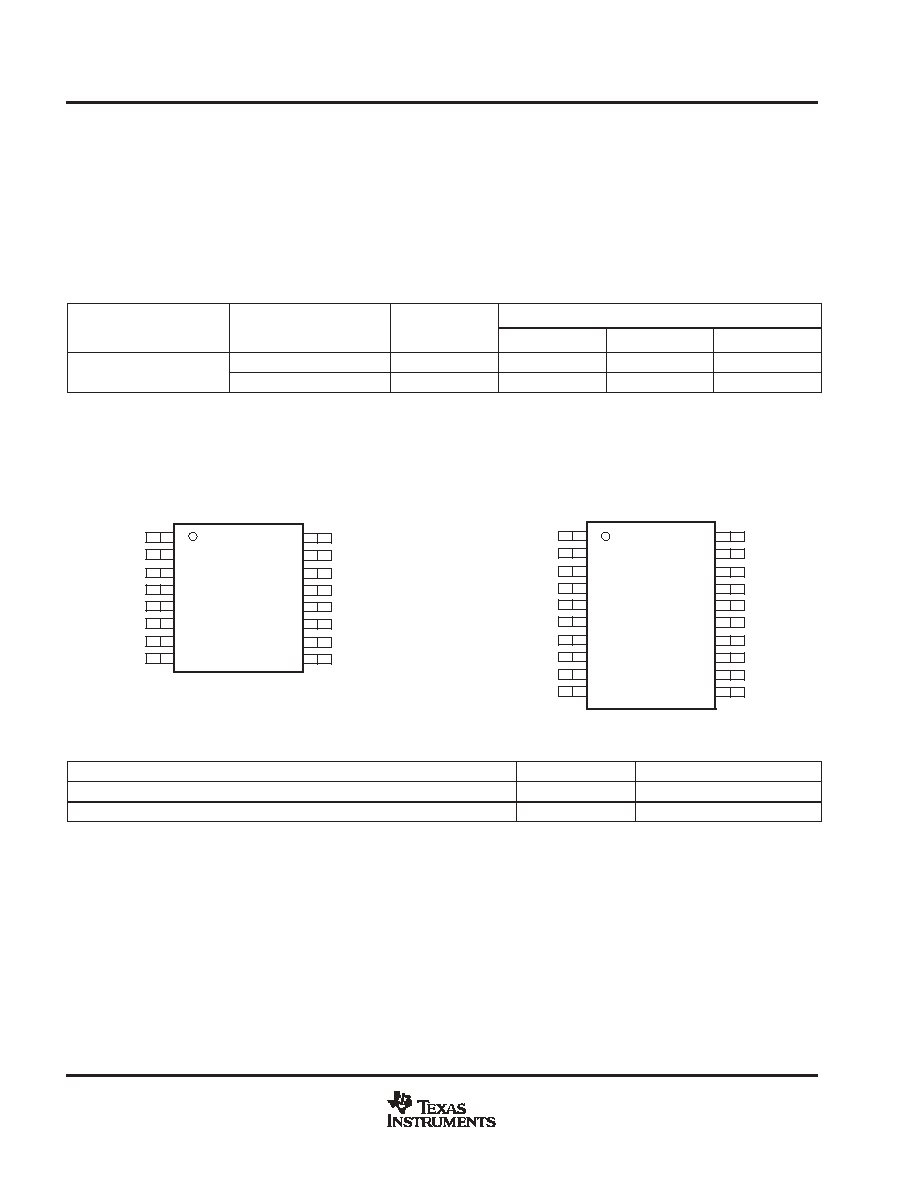
The UCC28220 is available in both 16-pin SOIC and low-profile TSSOP packages. The UCC28221 also comes
in 16-pin SOIC package and a slightly larger 20-pin TSSOP package to allow for high voltage pin spacing to
meet UL1950 creepage clearance safety requirements.
ORDERING INFORMATION
TEMPERATURE RANGE
UVLO THRESHOLDS
110-V HV JFET
STARTUP CIR-
PACKAGED DEVICES
TEMPERATURE RANGE
TA = TJ
UVLO THRESHOLDS
STARTUP CIR-
CUIT
SOIC-16 (D)
TSSOP-16 (PW)
TSSOP-20 (PW)
-40
�
C to +105
�
C
10 V on / 8 V off
NO
UCC28220D
UCC28220PW
-
-40
�
C to +105
�
C
13 V on / 8 V off
YES
UCC28221D
-
UCC28221PW
NOTE: D (SOIC) and PW (TSSOP) packages are available taped and reeled. Add R suffix to device type, e.g. UCC28220DR or UCC28221PWR.
The reel quanities are 2,500 devices per reel for D package and 2,000 devices per reel for the PW package.
CONNECTION DIAGRAM
1
2
3
4
5
6
7
8
16
15
14
13
12
11
10
9
LINEOV
LINEHYS
VDD
CS1
SLOPE
CS2
SS
CTRL
VIN (for UCC28221)
N/C (for UCC28220)
LINEUV
REF
OUT1
OUT2
GND
CHG
DISCHG
UCC28220D, UCC28220PW
and UCC28221D PACKAGE
(TOP VIEW)
1
2
3
4
5
6
7
8
9
10
20
19
18
17
16
15
14
13
12
11
N/C
LINEOV
LINEHYS
VDD
CS1
SLOPE
CS2
SS
CTRL
N/C
VIN
N/C
LINEUV
REF
OUT1
OUT2
GND
CHG
DISCHG
N/C
UCC28221PW PACKAGE
(TOP VIEW)
RECOMMENDED OPERATION CONDITIONS
Parameter
Symbol
Condition
High voltage start-up input
VIN
36 V to 76 V
Supply voltage
VDD
8 V to 14.5 V

UCC28220, UCC28221
SLUS544A - SEPTEMBER 2003 - REVISED AUGUST 2004
3
www.ti.com
ABSOLUTE MAXIMUM RATINGS
over operating free-air temperature (unless otherwise noted)
}
Parameter
UCC2822X
UNIT
High voltage start-up input, VIN
110
V
Supply voltage, VDD
15
V
Output current (OUT1, OUT2) dc , IOUT(dc)
�
10
mA
OUT1/ OUT2 capacitive load
200
pF
REF output current, IREF
10
mA
Current sense inputs, CS1, CS2
-1.0 to 2.0
V
Analog inputs (CHG, DISCHG, SLOPE, REF, CNTRL)
-0.3 to 3.6
V
Analog inputs (SS, LINEOV, LINEUV, LINEHYS)
-0.3 to 7.0
V
Power dissipation at TA = 25
�
C (PW package)
400
mW
Power dissipation at TA = 25
�
C (D package)
650
mW
Junction operating temperature, TJ
-55 to 150
�
C
Storage temperature, Tstg
-65 to 150
�
C
Lead temperature (soldering, 10 sec.), Tsol
300
�
C
Stresses beyond those listed under "absolute maximum ratings" may cause permanent damage to the device. These are stress ratings only, and
functional operation of the device at these or any other conditions beyond those indicated under "recommended operating conditions" is not
implied. Exposure to absolute-maximum-rated conditions for extended periods may affect device reliability.
All voltages are with respect to GND. Currents are positive into, negative out of the specified terminal. Consult Packaging Section of the Databook
for thermal limitations and considerations of packages.
ELECTRICAL CHARACTERISTICS:
V
DD
= 12 V, 0.1-
�
F capacitor from VDD to GND, 0.1-
�
F capacitor from REF to GND, F
OSC
= 1 MHz, T
A
= -40
�
C to
105
�
C, T
A
= T
J
, (unless otherwise noted).
PARAMETER
TEST CONDITION
MIN
TYP
MAX
UNITS
Overall Section
Operating VDD range
8
14
V
Quiescent current
SS = 0 V, no switching, Fosc = 1 MHz
1.5
3
4
mA
Operating current
Outputs switching, Fosc = 1 MHz
1.6
3.5
6
mA
Startup Section
Startup current
UCC28220 VDD < (UVLO-0.8)
200
A
Startup current
UCC28221 VDD < (UVLO-0.8)
500
�
A
UVLO start threshold
UCC28220
9.5
10
10.5
UVLO start threshold
UCC28221
12.3
13
13.7
V
UVLO stop threshold
7.6
8
8.4
V
UVLO hysteresis
UCC28220
1.8
2
2.2
V
UVLO hysteresis
UCC28221
4.8
5
5.2
JFET ON threshold
SS = 0, outputs not switching, VDD decreasing
9.5
10
10.5
V
JFET ON threshold
SS = 2 V,Cntrl = 2 V, output switching, VDD decreasing;
same threshold as UVLO stop
7.6
8
8.4
V
High voltage JFET current
VIN = 36 V to 76 V, VDD = 0 V
16
48
100
High voltage JFET current
VIN = 36 V to 76 V, VDD = 10 V
4
16
40
mA
High voltage JFET current
VIN = 36 V to 76 V, VDD < UVLO
4
12
40
mA
JFET leakage
VIN = 36 V to 76 V, VDD = 14 V
100
�
A
UCC28220, UCC28221
SLUS544A - SEPTEMBER 2003 - REVISED AUGUST 2004
4
www.ti.com
ELECTRICAL CHARACTERISTICS:
V
DD
= 12 V, 0.1-
�
F capacitor from VDD to GND, 0.1-
�
F capacitor from REF to GND, F
OSC
= 1 MHz, T
A
= -40
�
C to
105
�
C, T
A
= T
J
, (unless otherwise noted).
PARAMETER
TEST CONDITION
MIN
TYP
MAX
UNITS
Reference
Output voltage
8 V < VDD < 14 V, ILOAD=0 mA to -10 mA
3.15
3.3
3.45
V
Output current
Outputs not switching; CNTRL = 0 V
10
mA
Ouput short circuit current
VREF = 0 V
-40
-20
-10
mA
VREF UVLO
2.55
3
3.25
V
Soft-Start
SS charge current
RCHG=10.2 k
, SS = 0 V
-70
-100
-130
A
SS discharge current
RCHG=10.2 k
, SS = 2 V
70
100
130
�
A
SS initial voltage
LINEOV=2 V, LINEUV = 0 V
0.5
1
1.5
V
SS voltage at 0% dc
Point at which output starts switching
0.5
1.2
1.8
V
SS voltage ratio
75%
90%
100%
SS Max voltage
LINEOV = 0 V, LINEUV = 2 V
3
3.5
4
V
Oscillator and PWM
Output frequency
RCHG = 10.2 k
, RDISCHG = 10.2 k
450
500
550
kHz
Oscillator frequency
RCHG = 10.2 k
, RDISCHG = 10.2 k
900
1000
1100
kHz
Output maximum duty cycle
RCHG = 10.2 k
, RDISCHG = 10.2 k
, measured at OUT1
and OUT2
73%
75%
77%
%
CHG voltage
2
2.5
3
V
DISCHG voltage
2
2.5
3
V
Slope Compensation
Slope
RSLOPE = 75 k
, RCH = 66 k
, RDISCHG = 44 k
, Csx =
0 V to 0.5 V
140
200
260
mV/us
Channel matching
RSLOPE = 75 k
, Csx = 0 V
0%
10%
Current Sense
CS1, CS2 bias current
CS1 = 0, CS2 = 0
-500
0
500
nA
Prop delay CSx to OUTx
CSx input 0 V to 1.5 V step
40
85
ns
CS1, CS2 sink current
CSx = 2 V
2.3
4.5
7
mA
CNTRL Section
Resistor ratio(1)
0.6
Ctrl input current
CTRL = 0 V and 3.3 V
-100
0
100
nA
Ctrl voltage at 0% dc
CSx = 0 V, Point at which output starts switching (checks
resistor ratio)
0.5
1.2
1.8
V
NOTES: (1). Ensured by design. Not 100% tested in production.

UCC28220, UCC28221
SLUS544A - SEPTEMBER 2003 - REVISED AUGUST 2004
5
www.ti.com
ELECTRICAL CHARACTERISTICS:
V
DD
= 12 V, 0.1-
�
F capacitor from VDD to GND, 0.1-
�
F capacitor from REF to GND, F
OSC
= 1 MHz, T
A
= -40
�
C to
105
�
C, T
A
= T
J
, (unless otherwise noted).
PARAMETER
TEST CONDITION
MIN
TYP
MAX
UNITS
Output Section (OUT1, OUT2)
Low level
IOUT = 10 mA
0.4
1
V
High level
IOUT = -10 mA, VREF � VOUT
0.4
1
V
Rise time
CLOAD = 50 pF
10
20
ns
Fall time
CLOAD = 50 pF
10
20
ns
LINE Sense section
LINEOV threshold
TA = 25
�
C
1.240
1.260
1.280
LINEOV threshold
TA =-40
�
C to 105
�
C
1.235
1.260
1.285
LINEUV threshold
TA = 25
�
C
1.240
1.260
1.280
V
LINEUV threshold
TA =-40
�
C to 105
�
C
1.235
1.260
1.285
V
LINEHYST pull up voltage
LINEOV = 2 V, LINEUV = 2 V
3.1
3.25
3.4
LINEHYST off leakage
LINEOV = 0 V, LINEUV = 2 V
-500
0
500
nA
LINEHYS pull-up resistance
I = -20
�
A
100
500
LINEHYS pull-down resistance
I = 20
�
A
100
500
LINEOV, LINEUV bias I
LINEOV = 1.25 V, LINEUV = 1.25 V
-500
500
nA
NOTES: (1). Ensured by design. Not 100% tested in production.

UCC28220, UCC28221
SLUS544A - SEPTEMBER 2003 - REVISED AUGUST 2004
6
www.ti.com
FUNCTIONAL BLOCK DIAGRAM
14
REF
10
CHG
9
DISCHG
8
CTRL
4
CS1
6
CS2
5
SLOPE
2
LINEHYS
12
OUT2
11
GND
13
OUT1
7
SS
3
VDD
16
VIN
(N/C on
UCC28220)
SLOPE
COMPENSATION
S
Q
Q
R
+
CLK1
S
Q
Q
R
+
CLK2
OSC
20 k
30 k
1 pF
REFERENCE
UVLO/ JFET
CONTROL
RUN
Soft-Start
VREF
VREF
T
Q
Q
CLK1
CLK2
+
+
-
1
LINEOV
15 LINEUV
LINE OV/UV
RUN
LATCH
LATCH
+
+
0.5 V
0.5 V
RUN
RUN
P
2
FF
NOTE: Pinout for 16 pin option shown. See the 20-pin connection to UCC28221PW in the Terminal Functions table on the next page.

UCC28220, UCC28221
SLUS544A - SEPTEMBER 2003 - REVISED AUGUST 2004
7
www.ti.com
Terminal Functions
TERMINAL
PIN NUMBER
FUNCTION
UCC28220D
UCC28220PW
UCC28221D
UCC28221PW
NAME
I/O
FUNCTION
1
1
2
LINEOV
I
Input for line over voltage comparator
2
2
3
LINEHYS
I
Sets line comparator hysteresis
3
3
4
VDD
I
Device supply input
4
4
5
CS1
I
Channel 1 current sense input
5
5
6
SLOPE
I
Sets slope compensation
6
6
7
CS2
I
Channel 2 current sense input
7
7
8
SS
I
Soft-start input
8
8
9
CTRL
I
Feedback control input
9
9
12
DISCHG
I
Sets oscillator discharge current
10
10
13
CHG
I
Sets oscillator charge current
11
11
14
GND
-
Device ground
12
12
15
OUT2
O
PWM output from channel 2
13
13
16
OUT1
O
PWM output from channel 1
14
14
17
REF
O
Reference voltage output
15
15
18
LINEUV
I
Input for line under voltage comparator
-
16
20
VIN
I
High voltage start-up input
16
-
1, 10, 11, 19
N/C
-
No connection
PIN DESCRIPTIONS
VDD: This is used to supply power to the device, monitoring this pin is a the UVLO circuit. This is used to insure
glitch-free startup operation. Until VDD reaches its UVLO threshold, it remains in a low power mode, drawing
approximately 150
�
A of current and forcing pins, SS, CS1, CS2, OUT1, and OUT2 to logic 0 states. If the VDD
falls below 8 V after reaching turn-on, it will go back into this low power state. In the case of the UCC28221, the
UVLO threshold is 13 V. It is 10 V for the UCC28220. Both versions have a turn-off threshold of 8 V.
VIN (UCC28221 only): This pin has an internal high voltage JFET used for startup. The drain is connected to
VIN, while its' source is connected to VDD. During startup, this JFET delivers 12 mA typically with a minimum
of 4 mA to VDD, which in turn, charges up the VDD bypass capacitor. When VDD gets to 13 V, the JFET is turned
off.
CS1 and CS2: These 2 pins are the current sense inputs to the device. The signals are internally level shifted
by 0.5 V before the signal gets to the PWM comparator. Internally the slope compensation ramp is added to this
signal. The linear operating range on this input is 0 to 1.5 V. Also, this pin gets pulled to ground each time its
respective output goes low. (ie: OUT1 and OUT2).
SLOPE: This pin sets up a current used for the slope compensation ramp. A resistor to ground sets up a current,
which is internally divided by 25 and then applied to an internal 10-pF capacitor. Under normal operation th dc
voltage on this pin is 2.5 V..
SS: A capacitor to ground sets up the soft-start time for the open loop soft-start function. The source and sink
current from this pin is equal to 3/7th of the oscillator charge current set by the resistor on the CHG pin. The
soft start capacitor is held low during UVLO and during a Line OV or UV condition. Once an OV or UV fault
occurs, the soft-start capacitor is discharged by a current equal to its charging current. The capacitor does NOT
quickly discharge during faults. In this way, the controller has the ability to recover quickly from very short line
transients. This pin can also be used as an Enable/Disable function.

UCC28220, UCC28221
SLUS544A - SEPTEMBER 2003 - REVISED AUGUST 2004
8
www.ti.com
CHG: A resistor from this pin to GND sets up the charging current of the internal C
T
capacitor used in the
oscillator. This resistor, in conjunction with the resistor on the DISCHG pin is used to set up the operating
frequency and maximum duty cycle. Under normal operation the dc voltage on this pin is 2.5 V.
DISCHG: A resistor from this pin to GND sets up the discharge current of the internal C
T
capacitor used in the
oscillator. This resistor, in conjunction with the resistor on the CHG pin is used to set up the operating frequency
and maximum duty cycle. Under normal operation the dc voltage on this pin is 2.5 V.
OUT1 and OUT2: These output buffers are intended to interface with high current MOSFET drivers. The output
drive capability is approximately 33 mA and has an output impedance of 100
. The outputs swing between
GND and REF.
LINEOV: This pin is connected to a comparator and used to monitor the line voltage for an over voltage
condition. The typical threshold is 1.26 V.
LINEUV: This pin is connected to a comparator and used to monitor the line voltage for an under voltage
condition. The typical threshold is 1.26 V.
LINEHYST: This pin is controlled by both the LINEOV and LINEUV pins. It is used to control the hysteresis
values for both the over and under voltage line detectors.
REF: REF is a 3.3-V output used primarily as a source for the output buffers and other internal circuits. It is
protected from accidental shorts to ground. For improved noise immunity it is recommended that the reference
pin be bypassed with a minimum of 0.1
�
F of capacitance to GND.
APPLICATION INFORMATION
General
The device is comprised of several housekeeping blocks as well as two slope compensated PWM channels that
are interleaved. The circuit is intended to run from an external VDD supply voltage between 8 V and 14 V,
however, the UCC28221 has the addition of a high voltage startup JFET with control circuitry which can be used
for system startup. Other functions contained in the device are supply UVLO, 3.3-V reference, accurate line OV
and UV functions, a high speed programmable oscillator for both frequency and duty cycle, programmable slope
compensation, and programmable soft start functions.
The UCC28220/1 is a primary side controller for a two channel interleaved power converter. The device is
compatible with forward or flyback converters as long as a duty cycle clamp between 60 and 90 percent is
required. The active clamp forward and flyback converters as well as the RCD and resonant reset forward
converters are therefore compatible with this device. To ensure the two channels share the total converter output
current, current mode control with internal slope compensation is used. Slope compensation is user
programmable via a dedicated pin and can be set over a 50:1 range, ensuring good small-signal stability over
a wide range of applications.

UCC28220, UCC28221
SLUS544A - SEPTEMBER 2003 - REVISED AUGUST 2004
9
www.ti.com
APPLICATION INFORMATION
LINE Over Voltage and Under Voltage
Three pins are provided to turn-off the output drivers and reset the soft-start capacitor when the converter input
voltage is outside a prescribed range. The under-voltage set point and under-voltage hysteresis are accurately
set via external resistors. The over-voltage set point is also accurately set via a resistor ratio, but the hysteresis
is fixed by the same resistor that sets the u*nder-voltage hysteresis.
Figure 1 and 2 show detailed functional diagram and operation of the under voltage lockout (UVLO) and
over-voltage lockout (OVLO) features. The equations for setting the thresholds defined in Figure 2 are:
V1
+
1.26
R1
(R2
)
R3)
)
1.26
V2
+
1.26
(R1
)
Rx)
Rx
, where Rx
+
R4 (R2
)
R3)
V4
+
1.26
(R1
)
R2
)
R3)
R3
V3
+
V4
*
1.26
R1
R4
The UVLO hysteresis and the OVLO hysteresis can then be calculated as V2 - V1 and V4 - V3, respectively.
By examining the design equations it becomes apparent that the value of R4 sets the amount of hysteresis at
both thresholds. By realizing this fact, the designer can then set the value of R4 based on the most critical
hysteresis specification either at high line or at low line. In most designs the value of R4 will be determined by
the desired amount of hysteresis around the UVLO threshold. As an example consider a telecom power supply
with the following input UVLO and OVLO design specifications:
�
V1 = 32.0 V
�
V2 = 34.0 V
�
V3 = 83.0 V
�
V4 = 84.7 V
Then,
�
R1 = 976 k
�
R2 = 24.9 k
�
R3 = 15.0 k
and
�
R4 = 604 k
(1)
(2)
(3)
(4)

UCC28220, UCC28221
SLUS544A - SEPTEMBER 2003 - REVISED AUGUST 2004
10
www.ti.com
APPLICATION INFORMATION
15
1
2
R2
R1
R3
Input
Voltage
+
UV
HYS
OV
+
1.26 V
+
1.26 V
LINE_GOOD
S1
OPEN
S2
CLOSED
1.26 V
R4
Figure 1. Line UVLO and OVLO Functional Diagram
V1
V2
V3
V4
LINE_GOOD
ENABLE
OFF
Figure 2. Line UVLO and OVLO Operation
VDD
Because the driver output impedance is high the energy storage requirements on the VDD capacitor is low. For
improved noise immunity it is recommended that the VDD pin, be bypassed with a minimum of 0.1
�
F of
capacitance to GND. In most typical applications the bias voltage for the MOSFET drivers will also be used as
the VDD supply voltage for the chip. In the aforementioned applications it is beneficial to add a low valued
resistor between the bulk storage capacitor of the driver and the VDD capacitor for the UCC28220/1. By adding
a resistor in series with the bias supply any noise that is present on the bias supply will be filtered out before
getting to the VDD pin of the controller.

UCC28220, UCC28221
SLUS544A - SEPTEMBER 2003 - REVISED AUGUST 2004
11
www.ti.com
APPLICATION INFORMATION
Reference
For improved noise immunity it is recommended that the reference pin, REF, be bypassed with a minimum of
0.1uF of capacitance to GND.
Oscillator Operation and Maximum Duty Cycle Setpoint
The oscillator uses an internal capacitor to generate the time base for both PWM channels. The oscillator is
programmable over a 200 kHz to 2MHz frequency range with 20% to 80% maximum duty cycle range. Both the
dead time and the frequency of the oscillator are divided by 2 to generate the PWM clock and off-time information
for each of the outputs. In this way, a 20% oscillator duty cycle corresponds to a 60% maximum duty cycle at
each output, where an 80% oscillator duty cycle yields a 90% duty cycle clamp at each output.
The design equations for the oscillator and maximum duty cycle set point are given by:
F
OSC
+
2
F
OUT
D
MAX(osc)
+
1
*
2
1
*
D
MAX(out)
R
CHG
+
K
OSC
D
MAX(osc)
F
OSC
R
DISCHG
+
K
OSC
1
*
D
MAX(osc)
F
OSC
Where:
�
K
OSC
= 2.04 x 10
10
[
/
s]
�
F
OUT
= Switching frequency at the outputs of the chip [Hz]
�
D
MAX(out)
= Maximum duty cycle limit at the outputs of the chip
�
D
MAX(osc)
= Maximum duty cycle of the Oscillator for the desired maximum duty cycle at the outputs
�
F
OSC
= Oscillator frequency for desired output frequency [Hz]
�
R
CHG
= External oscillator resistor which sets the charge current - [
]
�
R
DISCHG
= External oscillator resistor which sets the discharge current - [
]
Start-Up JFET Section
A 110-V start-up JFET is included to start the device from a wide range (36 V-75 V) telecom input source. When
VDD is lower than 13 V the JFET is on, behaving as a current source charging the bias capacitors on VDD and
supplying current to the device. In this way, the VDD bypass capacitors are charged to 13 V where the outputs
start switching and the JFET is turned off. To enable a constant bias supply to the device during a pulse skipping
condition, the JFET is turned back on whenever VDD decreases below 10 V and the outputs are not switching.
Thus, the current from the JFET can overcome the internal bias currents, as long as the device is not actively
switching the output drivers. See Figure 2 below for a graphical representation of the JFET/VDD operation. The
UCC28220 does not contain an internal JFET and has a startup threshold of 10 V which makes it capable of
directly operating off a 12 V dc bus
(5)
(6)
(7)
(8)

UCC28220, UCC28221
SLUS544A - SEPTEMBER 2003 - REVISED AUGUST 2004
12
www.ti.com
APPLICATION INFORMATION
VDD
HV JFET
OUTx
GATE DRV
ON
0V
8 - 14 V
13 V
10 V
OFF
ON
OFF
8 V (UVLO off)
13 V
NORMAL OPERATION
Figure 3. JFET Device Operation with VDD Voltage
Soft-Start
A current is forced out of the SS pin, equal to 3/7 of the current set by R
CHG
, to provide a controlled ramp voltage.
The current set by the R
CHG
resistor is equal to 2.5 V divided by R
CHG
. This ramp voltage overrides the
commanded duty cycle on the CTRL pin, allowing a controlled start-up. Assuming the UCC28221 is biased on
the primary side, the soft start should be quite quick to allow the secondary bias to be generated and the
secondary side control can then take over. Once the soft-start time interval is complete, a closed loop soft-start
on the secondary side can be executed.
ISS
+
3
7
2.5
R
CHG
where,
ISS = current which is sourced out of the SS pin during the soft-start time - [Amps]
Current Sense
The current sense signals CS1 and CS2 are level shifted by 0.5 V and have the slope compensation ramps
added to them before being compared to the control voltage at the input of the PMW comparators. The
amplitude of the current sense signal at full load should be selected such that it is very close to the maximum
control voltage in order to limit the peak output current during short circuit operation.
Output Drivers
The UCC28220/1 is intended to interface with the UCC27323/4/5 family of MOSFET drivers. As such, the output
drive capability is low, effectively 100
and the driver outputs swing between GND and REF.
(9)

UCC28220, UCC28221
SLUS544A - SEPTEMBER 2003 - REVISED AUGUST 2004
13
www.ti.com
APPLICATION INFORMATION
Slope Compensation
The slope compensation circuit in the UCC28220/1 operates on a cycle-by-cycle basis. The two channels have
separate slope compensation circuits. These are fabricated in precisely the same way so as current sharing
is unaffected by the slope compensation circuit. For each channel, an internal capacitor is reset whenever that
channel's output is off. At the beginning of the PWM cycle, a current is mirrored off the SLOPE pin into the
capacitor, developing an independent ramp. Since the two channel's ramps will start when the channel's output
changes from a low to high state, the ramps are thus interleaved. These internal ramps are added to the voltages
on the current sense pins, CS1 and CS2 and the result forms an input to the PWM comparators.
PWM
CS1
(4)
+
-
REF
CTRL
(8)
+
SLOPE
(5)
C_SC
OUT 1
TO RESET
of
PWM LATCH
ON OFF
2.5/(25*R_SLOPE) = I_SC
R_SLOPE
0.5V
10 pF
S1
S2
Figure 4. Slope Compensation Detail for Channel 1. Duplicate Matched Circuitry Exists for Channel 2.
To ensure stability, the slope compensation circuit must add between 1/5 and 1 times the inductor downslope
to each of the current sense signals prior to being applied to the PWM comparator's input.

UCC28220, UCC28221
SLUS544A - SEPTEMBER 2003 - REVISED AUGUST 2004
14
www.ti.com
APPLICATION INFORMATION
Determining the value for the slope compensation resistor:
Design Example:
NCT(p) = 1
VOUT = 12
Np = 7
RSENSE = 5.23
FS(out) = 500000
NCT(s) = 50
LOUT = 3.2 x 10 -6
Ns = 5
VEA(cl) = 1.98
FS(out) = 500000
Where,
�
N
CT(p)
= Number of primary turns on the Current Transformer - [Turns]
�
N
CT(s)
= Number of Secondary turns on the current transformer - [Turns]
�
V
OUT
= Nominal output voltage of the converter - [V]
�
L
OUT
= Inductance value of each output inductor - [H]
�
N
P
= Number of primary turns on the main transformer - [Turns]
�
N
S
= Number of secondary turns on the main transformer - [Turns]
�
R
SENSE
= Value of current sense resistor on secondary of current sense transformer - [Ohms]
�
V
EA(cl)
= Maximum Value of the E/A output voltage - [Volts]
�
F
S(out)
= Switching frequency of each output - [Hz]
Determine the correct value for the slope resistor, R
SLOPE
, to provide the desired amount of slope
compensation.
N
CT
+
N
CT(p)
N
CT(s)
, Current Transformer Turns Ratio
1.
Transform the Secondary Inductor Downslope to the Primary
S
L(prime)
+
V
OUT
L
OUT
N
s
N
p
,
S
L(prime)
+
2.679 A
m
s
2.
Calculate the Transformed Slope Voltage at Sense Resistor:
VS
L(prime)
+
S
L(prime)
N
CT
R
SENSE
,
VS
L(prime)
+
2.281 V
m
s
3.
Calculate the R
SLOPE
value to give a compensating ramp equal to the transformed slope voltage given
above.:
M
+
1.0
Desired ratio between the compensating ramp and the output inductor downslope ramp, transformed to the
primary sense resistor
R
SLOPE
+
10
4
M
VS
L(prime)
10
*
6
,
R
SLOPE
+
35.556 k
W

UCC28220, UCC28221
SLUS544A - SEPTEMBER 2003 - REVISED AUGUST 2004
15
www.ti.com
TYPICAL APPLICATION CIRCUITS
UCC28221
3
7
6
4
5
1
8
15
11
12
14
13
9
10
VDD
CS1
SLOPE
CS2
SS
CTRL
OV
UV
OUT1
OUT2
CHG
DISCHG
Bias
E/A
2
16
HYS
VIN
REF
GND
REF
1/2 UCC27424
1/2 UCC27424
CS1
CS2
VIN
VOUT
Figure 5. Interleaved Flyback Application Circuit Using the UCC28221

UCC28220, UCC28221
SLUS544A - SEPTEMBER 2003 - REVISED AUGUST 2004
16
www.ti.com
UCC28220
3
7
6
4
5
1
8
15
11
12
14
13
9
10
VDD
CS1
SLOPE
CS2
SS
CTRL
OV
UV
OUT1
OUT2
CHG
DISCHG
Bias
E/A
2
16
HYS
N/C
REF
GND
1/2 UCC27424
1/2 UCC27424
CS2
CS1
VIN
VOUT
Figure 6. Interleaved Boost Application Circuit Using the UCC28220

UCC28220, UCC28221
SLUS544A - SEPTEMBER 2003 - REVISED AUGUST 2004
17
www.ti.com
TYPICAL CHARACTERISTICS
Figure 7
UVLO THRESHOLDS
vs
TEMPERATURE
-50
-25
0
25
50
75
100
125
7.5
8.5
9.5
10.5
11.5
12.5
13.5
V
UVLO
- UVLO Thresholds- V
Tj - Temperature -
�
C
UCC28221 UVLO on threshold
UCC28220 UVLO on threshold and UCC28221
JFET on threshold (when not switching)
UCC28220 and UCC28221 UVLO off threshold and
UCC28221 JFET on threshold (when switching)
Figure 8
QUIESCENT CURRENT
vs
SUPPLY VOLTAGE
I DD
- Quiescent
Current - mA
0
2
4
6
8
10
12
14
0.0
0.5
1.0
1.5
2.0
2.5
3.0
16
3.5
4.0
VDD - Supply Voltage - V
UCC28221 EXCLUDES JFET CURRENT
UCC28220
UCC28221
Figure 9
SUPPLY CURRENT
vs
SUPPLY VOLTAGE
0
2
4
6
8
10
12
14
-50
-40
-30
-20
-10
0
10
16
20
30
I DD
- Supply Current - mA
VDD - Supply Voltage - V
UCC28221
V
IN
= 36 V
JFET source current
Figure 10
REFERENCE VOLTAGE
vs
TEMPERATURE
VREF - ReferenceV
oltage - V
-50
-25
0
25
50
75
100
3.15
3.20
3.25
3.30
3.35
3.40
3.45
125
Tj - Temperature -
�
C
No Load
Load

UCC28220, UCC28221
SLUS544A - SEPTEMBER 2003 - REVISED AUGUST 2004
18
www.ti.com
TYPICAL CHARACTERISTICS
Figure 11
LINEOV AND LINEUV THRESHOLDS
vs
TEMPERATURE
Vth
-
T
rip Threshold - V
-50
-25
0
25
50
75
100
1.230
1.235
1.240
1.245
1.250
1.255
1.260
125
1.265
1.270
Tj - Temperature -
�
C
LINEOV
LINEUV
Figure 12
SLOPE COMPENSATION
vs
TEMPERATURE
-50
-25
0.0
25
50
75
100
125
170
175
180
185
190
195
200
205
210
215
220
225
230
Tj - Temperature -
�
C
SLOPE - Slope Compensation - mV per
�
s
R
SLOPE
= 75 k
CS1 = 0 V
CS1 = 0.5 V
Figure 13
PROGRAMMING RESISTOR
vs
SLOPE COMPENSATION
10
100
1000
SLOPE - Slope Compensation - mV per
�
s
R
SLOPE
- Slope Programming Resistor -
106
105
104
103
Figure 14
CHANNEL1 AND CHANNEL2 SLOPE MATCHING
vs
TEMPERATURE
Mismatch
-
%
-10
-8
-6
-4
-2
0
2
4
6
8
10
-50
-25
0.0
25
50
75
100
125
Tj - Temperature -
�
C
R
SLOPE
= 75 k
CS0 = 0 V
CS1 = 0 V

UCC28220, UCC28221
SLUS544A - SEPTEMBER 2003 - REVISED AUGUST 2004
19
www.ti.com
TYPICAL CHARACTERISTICS
Figure 15
RISE AND FALL TIME
vs
TEMPERATURE (CL = 50 pf)
T
r
and Tf - Rise and Fall T
ime - ns
-50
-25
0
25
50
75
100
0
1
2
3
4
5
6
125
7
8
9
10
11
12
13
14
15
16
17
18
19
20
Tj - Temperature -
�
C
Fall Time
Rise Time
Figure 16
VOH AND VOL
vs
TEMPERATURE
V
O
-
Output
V
oltage
- V
-50
-25
0
25
50
75
100
0.0
0.1
0.2
0.3
0.4
0.5
0.6
125
0.7
0.8
0.9
1.0
Tj - Temperature -
�
C
VREF - VOUT (VOH)
VOL
I
OUT
= 10 mA
Figure 17
SOFTSTART CHARGE CURRENT
vs
TEMPERATURE
ISSCH - Charge Current -
�
A
-50
-25
0
25
50
75
100
-130
-120
-110
-100
-90
-80
-70
125
Tj - Temperature -
�
C
R
CHG
= 10.2 k
Figure 18
SOFTSTART DISCHARGE CURRENT
vs
TEMPERATURE
-50
-25
0
25
50
75
100
125
70
80
90
100
110
120
130
Tj - Temperature -
�
C
ISSdis - Charge Current -
�
A

UCC28220, UCC28221
SLUS544A - SEPTEMBER 2003 - REVISED AUGUST 2004
20
www.ti.com
TYPICAL CHARACTERISTICS
Figure 19
PROGRAMMING RESISTORS
vs
SWITCHING FREQUENCY
RCHRG RDISRG - Resistance -
fS -
Switching Frequency
- Hz
10K
100K
1M
1K
10K
100K
10M
1M
RCHRG = RDISRG
D
MAX
= 75%
Figure 20
OSCILLATOR FREQUENCY
vs
TEMPERATURE
f S
-
Oscillator Frequency
-
kHz
-50
-25
0
25
50
75
100
450
460
470
480
490
500
510
125
520
530
540
550
Tj - Temperature -
�
C
RCHRG = RDISRG = 10.2 k
Figure 21
PROGRAMMABLE MAX DUTY CYCLE
vs
TEMPERATURE
D
C
- Duty Cycle - %
-50
-25
0
25
50
75
100
73
74
75
76
77
125
Tj - Temperature -
�
C
RCHRG = RDISRG = 10.2 k
Figure 22
CSx to OUTx delay
vs
CSx Peak Voltage
CSx to OUTx delay - ns
CSx - Peak Voltage - V
0
0.2
0.4
0.6
0.8
1.0
1.2
0
10
20
30
40
50
60
1.4
70
80
90
100
1.6
1.8
105
�
C
25
�
C
-40
�
C

UCC28220, UCC28221
SLUS544A - SEPTEMBER 2003 - REVISED AUGUST 2004
21
www.ti.com
APPLICATION INFORMATION
Related Products
DEVICE
DESCRIPTION
PACKAGE OPTION
UCC27323/4/5
Dual 4-A High Speed Low Side MOSFET Drivers
SOIC-8, PowerPAD MSOP-8, PDIP-8
UCC27423/4/5
Dual 4-A High Speed Low Side MOSFET Drivers
with Enable
SOIC-8, PowerPAD MSOP-8, PDIP-8
TPS2811/12/13
Dual 2.4-A High Speed Low Side MOSFET Drivers
SOIC-8, TSSOP-8, PDIP-8
UC3714/15
Dual 2.4-A High Speed Low Side MOSFET Drivers
SOIC-8, PowerSOIC-14, PDIP-8
References and Resources:
An evaluation module and an associated user's guide are available. The UCC28221 is used in a two-channel
interleaved Forward design converting from 36-V to 76-V dc input voltage to a regulated 12-V dc output. The
power module has two isolated 100 W forward power stages operating at 500 kHz, which are operating 180
degrees out of phase with each other allowing for output current ripple cancellation and smaller magnetic
design. This design also takes advantage of the UCC28221's on-board 110-V internal JFET start up circuit that
removes the need of an external trickle charge resistor for boot strapping. This circuit turns off after auxiliary
power is supplied to the device conserving power.
D
Evaluation Module, UCC28221EVM, 48 V
IN
, 12 V
OUT
, 200-W Interleaved Forward Converter
D
User's Guide, UCC28221 Evaluation Module, Texas Instruments Literature Number SLUU173

UCC28220, UCC28221
SLUS544A - SEPTEMBER 2003 - REVISED AUGUST 2004
22
www.ti.com
MECHANICAL DATA
D (R-PDSO-G**)
PLASTIC SMALL-OUTLINE
PACKAGE
8 PINS SHOWN
8
0.197
(5,00)
A MAX
A MIN
(4,80)
0.189
0.337
(8,55)
(8,75)
0.344
14
0.386
(9,80)
(10,00)
0.394
16
DIM
PINS **
4040047/E 09/01
0.069 (1,75) MAX
Seating Plane
0.004 (0,10)
0.010 (0,25)
0.010 (0,25)
0.016 (0,40)
0.044 (1,12)
0.244 (6,20)
0.228 (5,80)
0.020 (0,51)
0.014 (0,35)
1
4
8
5
0.150 (3,81)
0.157 (4,00)
0.008 (0,20) NOM
0
�
- 8
�
Gage Plane
A
0.004 (0,10)
0.010 (0,25)
0.050 (1,27)
NOTES: A. All linear dimensions are in inches (millimeters).
B. This drawing is subject to change without notice.
C. Body dimensions do not include mold flash or
protrusion, not to exceed 0.006 (0,15).
D. Falls within JEDEC MS-012

UCC28220, UCC28221
SLUS544A - SEPTEMBER 2003 - REVISED AUGUST 2004
23
www.ti.com
MECHANICAL DATA
PW (R-PDSO-G**)
PLASTIC SMALL-OUTLINE
PACKAGE
14 PINS SHOWN
0,65
M
0,10
0,10
0,25
0,50
0,75
0,15 NOM
Gage Plane
28
9,80
9,60
24
7,90
7,70
20
16
6,60
6,40
4040064/F 01/97
0,30
6,60
6,20
8
0,19
4,30
4,50
7
0,15
14
A
1
1,20 MAX
14
5,10
4,90
8
3,10
2,90
A MAX
A MIN
DIM
PINS **
0,05
4,90
5,10
Seating Plane
0
�
- 8
�
NOTES: A. All linear dimensions are in millimeters.
B. This drawing is subject to change without notice.
C. Body dimensions do not include mold flash or
protrusion not to exceed 0,15.
D. Falls within JEDEC MO-153

IMPORTANT NOTICE
Texas Instruments Incorporated and its subsidiaries (TI) reserve the right to make corrections, modifications,
enhancements, improvements, and other changes to its products and services at any time and to discontinue
any product or service without notice. Customers should obtain the latest relevant information before placing
orders and should verify that such information is current and complete. All products are sold subject to TI's terms
and conditions of sale supplied at the time of order acknowledgment.
TI warrants performance of its hardware products to the specifications applicable at the time of sale in
accordance with TI's standard warranty. Testing and other quality control techniques are used to the extent TI
deems necessary to support this warranty. Except where mandated by government requirements, testing of all
parameters of each product is not necessarily performed.
TI assumes no liability for applications assistance or customer product design. Customers are responsible for
their products and applications using TI components. To minimize the risks associated with customer products
and applications, customers should provide adequate design and operating safeguards.
TI does not warrant or represent that any license, either express or implied, is granted under any TI patent right,
copyright, mask work right, or other TI intellectual property right relating to any combination, machine, or process
in which TI products or services are used. Information published by TI regarding third-party products or services
does not constitute a license from TI to use such products or services or a warranty or endorsement thereof.
Use of such information may require a license from a third party under the patents or other intellectual property
of the third party, or a license from TI under the patents or other intellectual property of TI.
Reproduction of information in TI data books or data sheets is permissible only if reproduction is without
alteration and is accompanied by all associated warranties, conditions, limitations, and notices. Reproduction
of this information with alteration is an unfair and deceptive business practice. TI is not responsible or liable for
such altered documentation.
Resale of TI products or services with statements different from or beyond the parameters stated by TI for that
product or service voids all express and any implied warranties for the associated TI product or service and
is an unfair and deceptive business practice. TI is not responsible or liable for any such statements.
Following are URLs where you can obtain information on other Texas Instruments products and application
solutions:
Products
Applications
Amplifiers
amplifier.ti.com
Audio
www.ti.com/audio
Data Converters
dataconverter.ti.com
Automotive
www.ti.com/automotive
DSP
dsp.ti.com
Broadband
www.ti.com/broadband
Interface
interface.ti.com
Digital Control
www.ti.com/digitalcontrol
Logic
logic.ti.com
Military
www.ti.com/military
Power Mgmt
power.ti.com
Optical Networking
www.ti.com/opticalnetwork
Microcontrollers
microcontroller.ti.com
Security
www.ti.com/security
Telephony
www.ti.com/telephony
Video & Imaging
www.ti.com/video
Wireless
www.ti.com/wireless
Mailing Address:
Texas Instruments
Post Office Box 655303 Dallas, Texas 75265
Copyright
2004, Texas Instruments Incorporated