 | –≠–ª–µ–∫—Ç—Ä–æ–Ω–Ω—ã–π –∫–æ–º–ø–æ–Ω–µ–Ω—Ç: UCC2839N | –°–∫–∞—á–∞—Ç—å:  PDF PDF  ZIP ZIP |
UCC2839
UCC3839
SLUS179A - APRIL 1999 - REVISED NOVEMBER 2001
FEATURES
∑ Practical Secondary Side Control of
Isolated Power Supplies
∑ Provides a Self Regulating Bias
Supply From a High Input Voltage
Using an External N-Channel
Depletion Mode FET
∑ Onboard Precision, Fixed Gain,
Differential Current Sense Amplifier
∑ Wide Bandwidth Current Error
Amplifier
∑ 5V Reference
∑ High Current, Programmable Gm
Amplifier Optimized to Drive
Opto-couplers
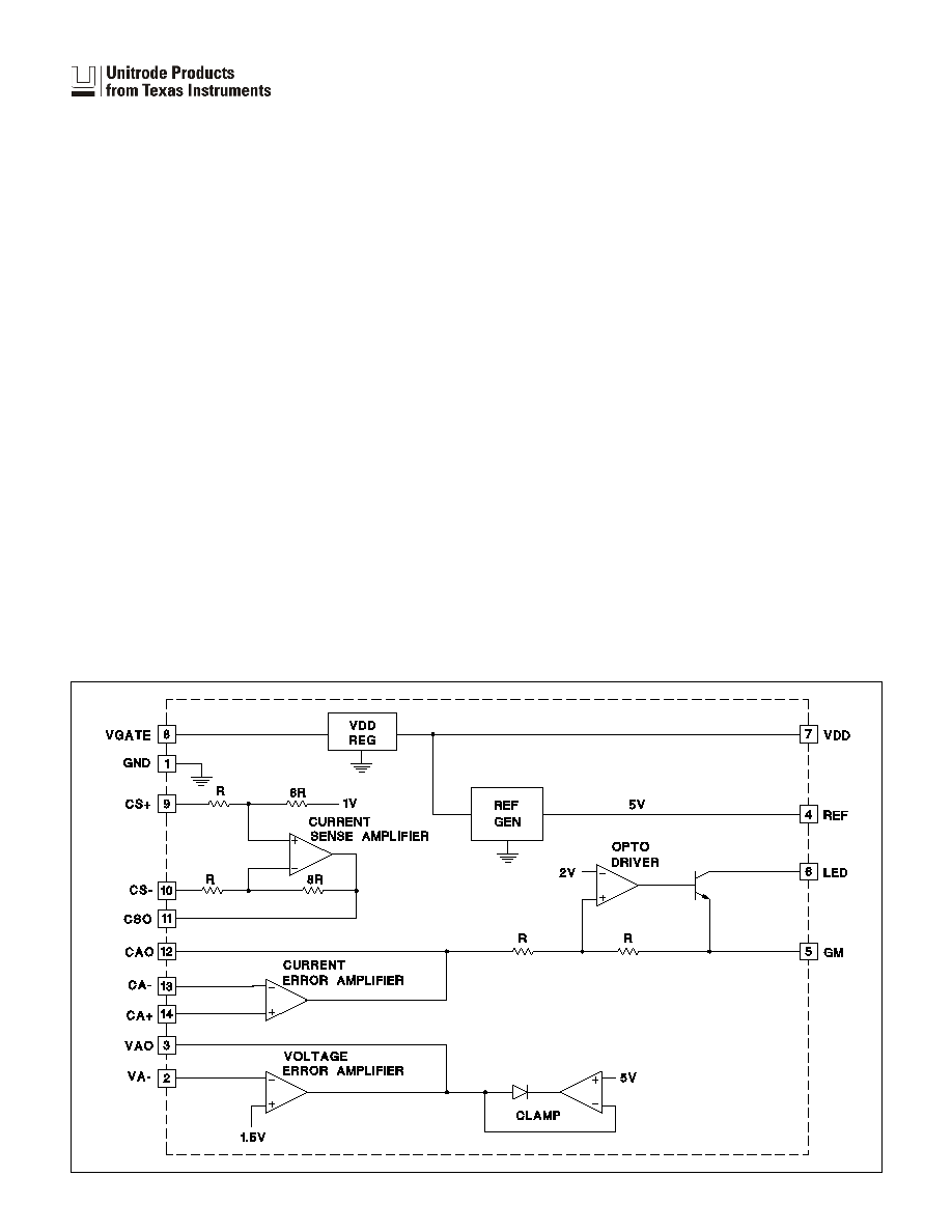
Secondary Side Average Current Mode Controller
BLOCK DIAGRAM
UDG-97011
DESCRIPTION
The UCC3839 provides the control functions for secondary side average
current mode control in isolated power supplies. Start up, pulse width mod-
ulation and MOSFET drive must be accomplished independently on the
primary side. Communication from secondary to primary side is antici-
pated through an opto-isolator.
Accordingly, the UCC3839 contains a fixed gain current sense amplifier,
voltage and current error amplifiers, and a Gm type buffer/driver amplifier
for the opto-isolator. Additional housekeeping functions include a precision
5V reference and a bias supply regulator.
Power for the UCC3839 can be generated by peak rectifying the voltage of
the secondary winding of the isolation transformer. From this unregulated
voltage, the UCC3839's bias supply regulator will generate its own 7.5V
bias supply using an external, N-channel, depletion mode FET.
The UCC3839 can be configured for traditional average current mode con-
trol where the output of the voltage error amplifier commands the current
error amplifier. It can also be configured for output voltage regulation with
average current mode short circuit current limiting, employing two parallel
control loops regulating the output voltage and output current independ-
ently.
2
UCC2839
UCC3839
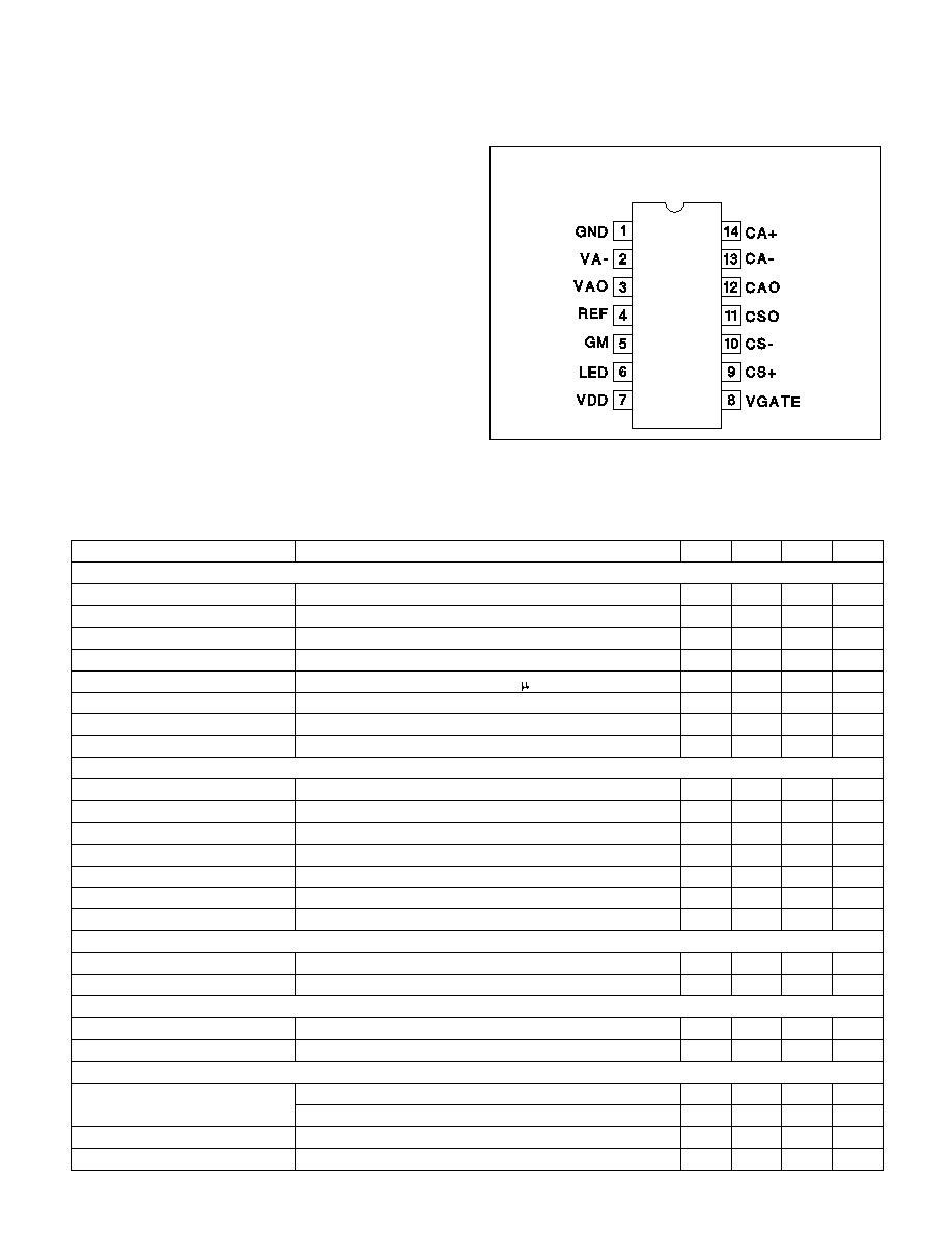
CONNECTION DIAGRAMS
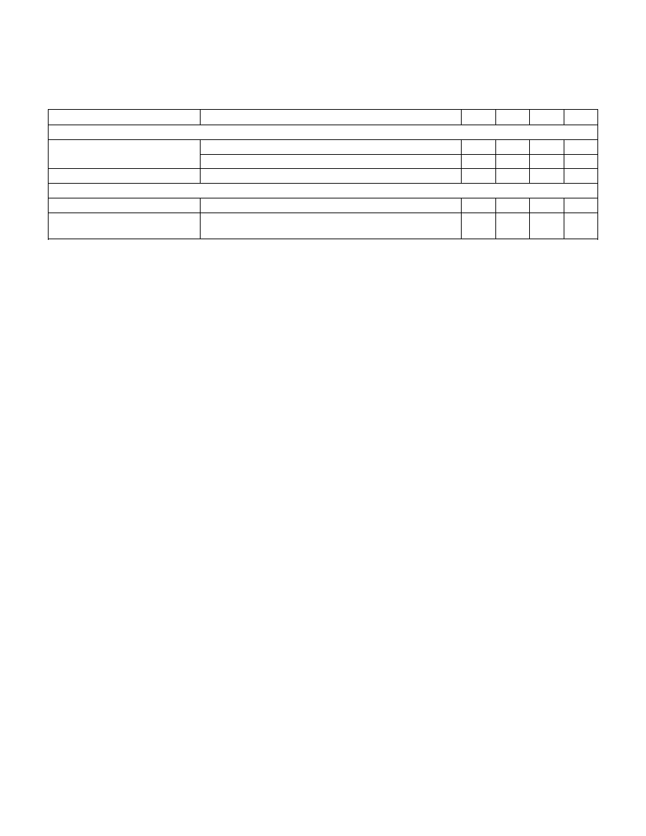
ELECTRICAL CHARACTERISTICS:
Unless otherwise specified, 0∞C to 70∞C for the UCC3839, ≠40∞C to 85∞ for the
UCC2839. V
LINE
= 10V, RG = 400
. T
A
= T
J
.
PARAMETER
TEST CONDITIONS
MIN
TYP
MAX
UNITS
Current Error Amplifier
VIO
10
mV
AVOL
60
dB
CMRR
V
CM
= 0.5V to 5.5V
60
dB
PSRR
V
LINE
= 10V to 20V
60
dB
CAO High
CA≠ = 1V, CA+ = 1.1V, I
CAO
= ≠100 A
4.8
7
V
I
CAO
CA≠ = 1V, CA+ = 1.1V, CAO = 0.5V
≠500
≠250
µA
CAO Low
CA≠ = 1V, CA+ = 0.9V, I
CAO
= 500
µA
0.2
0.4
V
GBW
F = 100kHz, T
A
= 25∞C
3
5
MHz
Voltage Error Amplifier
VA≠
1.46
1.5
1.525
V
AVOL
60
dB
PSRR
V
LINE
= 10V to 20V
60
dB
VAO High
I
VAO
= ≠100
µA to 100µA
4.8
5
5.2
V
I
VAO
VA≠ = 1.45V, VAO = 0.5V
≠500
≠250
µA
VAO Low
VA≠ = 1.55V, VAO = 0.5V, I
VAO
= 500
µA
0.2
0.4
V
GBW
(Note 1)
3
5
MHz
Current Sense Amplifier
CSO Zero
CS+ = CS≠ = ≠0.3V to 5.5V, I
CSO
= ≠100
µA to 100µA
0.85
1
1.15
V
AV
CS+ = 0, CS≠ = 0mV to ≠200mV
7.75
8
8.2
V/V
Current Sense Amplifier (cont.)
Slew Rate
CS+ = 0, CS≠ = 0mV to ≠0.5V
2
4
V/
µs
CSO
CS+ = ≠200mV, CS≠ = ≠700mV
4.75
5
5.2
V
LED Driver
I
LED
LED = 5.5V, CA≠ = 1V, CA+ = 1.1V, RG = 400
0
10
µA
LED = 5.5V, CA≠ = 1V, CA+ = 0.9V, RG = 400
9
10
11
mA
Gm
LED = 5.5V, CAO = 1V to 3V, RG = 400
2.25
2.5
2.75
mS
Slew Rate
CAO = 2V to 2.5V, LED = 400
to 5.5V, RG = 400
1
4
V/
µs
DIL-14, SOIC-14 (Top View)
D or N Package
ABSOLUTE MAXIMUM RATINGS
Supply Voltage . . . . . . . . . . . . . . . . . . . . . . . . . . . . . . . . . . 15V
Supply Current
(LED not connected) . . . . . . . . . . . . . . . . . . . . . . . . . . . 2mA
(LED connected) . . . . . . . . . . . . . . . . . . . . . . . . . . . . . 14mA
Analog Inputs . . . . . . . . . . . . . . . . . . . . . . . . . . . . ≠0.3V to 15V
Power Dissipation at T
A
= 60∞C
(LED not connected). . . . . . . . . . . . . . . . . . . . . . . . . . 20mW
(LED connected). . . . . . . . . . . . . . . . . . . . . . . . . . . . . 55mW
Storage Temperature . . . . . . . . . . . . . . . . . . . ≠65∞C to +150∞C
Junction Temperature . . . . . . . . . . . . . . . . . . . ≠55∞C to +150∞C
Lead Temperature (Soldering, 10sec.) . . . . . . . . . . . . . +300∞C
Currents are positive into, negative out of the specified terminal.
Consult Packaging Section of Databook for thermal limitations
and considerations of package.
3
UCC2839
UCC3839
ELECTRICAL CHARACTERISTICS:
Unless otherwise specified, 0∞C to 70∞C for the UCC3839, ≠40∞C to 85∞ for the
UCC2839. V
LINE
= 10V, RG = 400
. T
A
= T
J
.
PARAMETER
TEST CONDITIONS
MIN
TYP
MAX
UNITS
Precision Reference
REF
T
J
= 25∞C
4.94
5
5.06
V
I
REF
= 0mA to 1mA, V
LINE
= 10V to 20V
4.9
5.1
V
VA+/REF
0.298
0.3
0.302
V/V
VDD Regulator
VDD
IDD = 0mA to ≠15mA, V
LINE
= 10V to 40V
7
7.5
8
V
I
VDD
V
LINE
= 10V to 40V, CA≠ = 0V, CA+ = 1V, VA≠ = 2.9V, CS+
= CS≠ = 0, I
REF
= 0
1.3
2
mA
Note 1: Ensured by design. Not 100% tested in production.
CA≠: Current Error Amplifier Negative Input.
CAO: Current Error Amplifier Output. Output source cur-
rent is limited, and output sink current is guaranteed to
be greater than the VAO output source current. Current
loop compensation components are generally connected
to CAO and CA≠.
CA+: Current Error Amplifier Positive Input.
CS≠: Current Sense Amplifier Negative Input.
CSO: Current Sense Amplifier Output. Internally set gain
V
OUT
/V
IN
= 8 V
IN
= 0V results in CSO = 1V.
CS+: Current Sense Amplifier Positive Input.
GM: Gm (transconductance) Programming Pin. Resistor
R
GM
= 400
to GND.
GND: Chip Ground.
LED: Output of LED Driver. Connect LED from VDD pin
to LED.
REF: 5V Precision Reference Buffer Output. Minimum
Decoupling Capacitance = 0.01
µF
VA≠: Voltage Error Amplifier Negative Input. Voltage Er-
ror Amplifier is internally referenced to 1.5V
VAO: Voltage Error Amplifier Output. In a two loop aver-
age current mode control configuration, VAO is con-
nected to CA+ and is the current command signal. VAO
is internally clamped not to exceed 5V for short circuit
control. In a single loop voltage mode control configura-
tion with a parallel average short circuit current control
loop, VAO is connected directly to CAO. Output source
current is limited, and output sink current is guaranteed
to be greater than the CAO output source current.
VDD: 7.5V Regulator output. Supply for most of the chip.
Minimum Decoupling Capacitance = 0.01
µF
VGATE: External FET Gate Control Voltage.
PIN DESCRIPTIONS
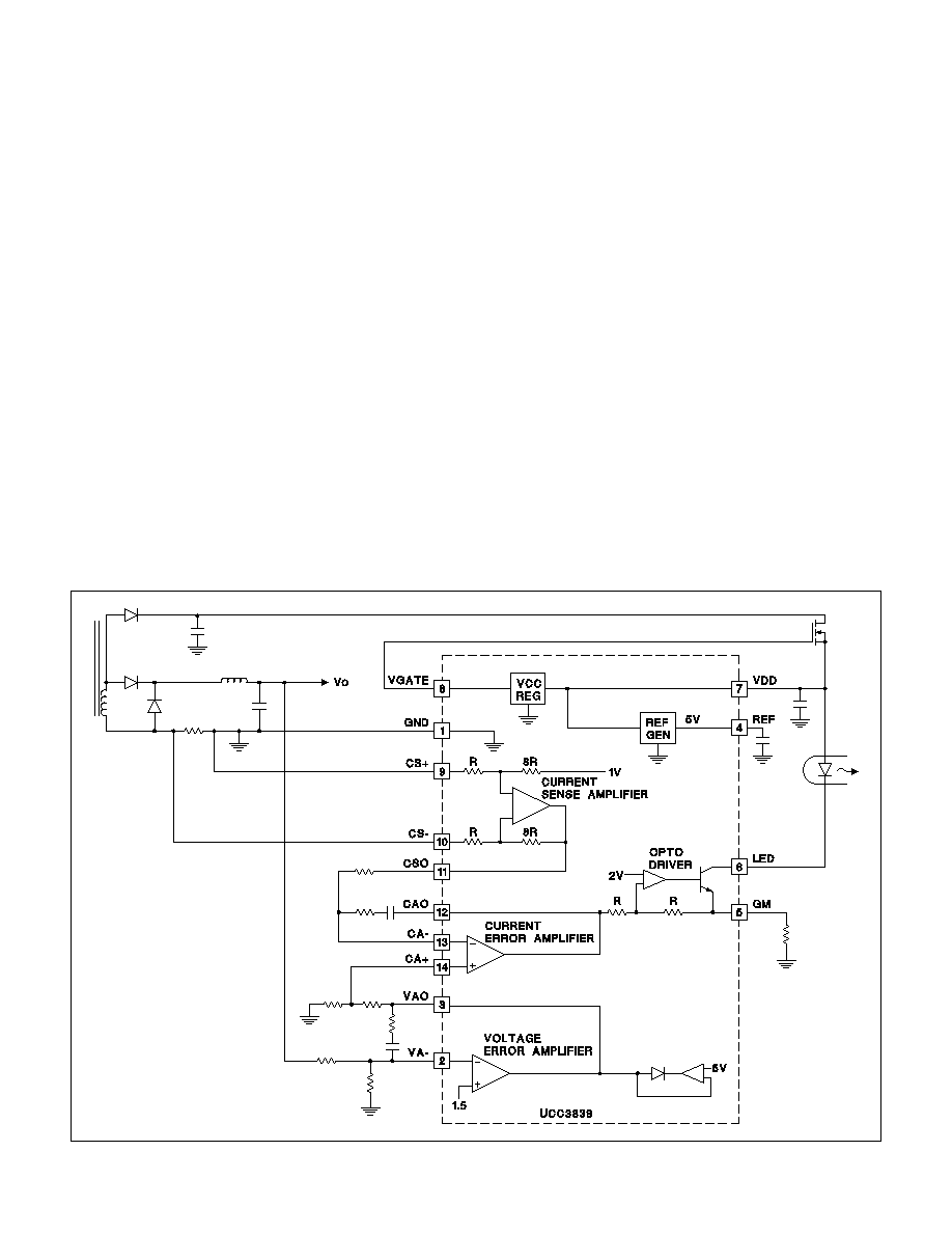
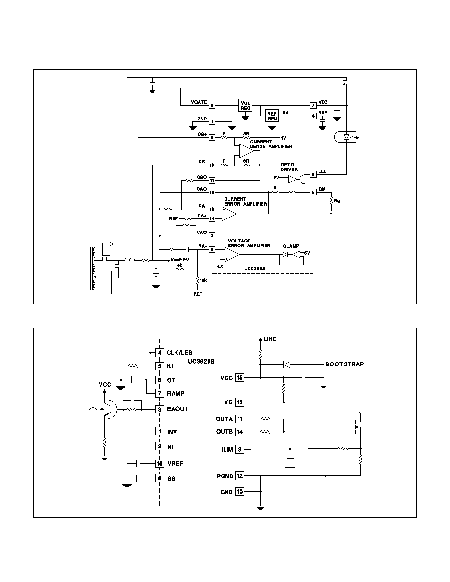
Fig. 1 shows a typical secondary side average current
mode controller configuration using the UCC3839. In this
configuration, output voltage is sensed and regulated by
the voltage error amplifier. Its output, VAO provides the
reference for the current error amplifier at the CA+ pin.
VAO can be connected to CA+ directly or through a re-
sistive divider depending on the particular application re-
quirements.
Average current mode control needs accurate output cur-
rent information which is provided by a low value current
sense resistor. The voltage proportional to the con-
verter's output current is sensed and amplified by the
precision current sense amplifier of the chip. The
onboard current sense amplifier has a gain of 8 and is in-
tended for differential sensing of the shunt voltage with a
common mode voltage range from 0V up to 5V. The out-
put of the current sense amplifier, CSO is 1V for zero in-
put which guarantees that the circuit can control currents
down to 0A.
The CSO signal is fed to the CA≠ input of the current er-
ror amplifier through a resistor. The current error amplifier
takes the VAO and CSO signals and generates the error
signal for the pulse width modulator.
APPLICATION INFORMATION
4
UCC2839
UCC3839
Figure 1. Secondary side average current mode controller.
UDG-97012
Since the PWM function is located on the primary side of
the power converter the CAO signal must be sent across
the safety isolation boundary. The UCC3839 anticipates
an opto-coupler to provide isolation between primary and
secondary. Therefore, CAO drives a transconductance
amplifier that controls LED current in an opto-isolator.
During start up and when CAO exceeds 4V, the current
in the LED drops to zero. Maximum LED current is ob-
tained during normal operation as CAO reaches its low-
est potential. Its value is determined by the programming
resistor value from the GM pin to circuit GND.
An alternative secondary side controller configuration is
introduced in Fig. 2. In this circuit, the voltage and current
control loops of the UCC3839 are connected parallel. It
can be achieved by connecting the VAO and CAO pins
together. The error amplifier with the lower output voltage
controls the current in the opto-coupler providing the
feedback signal for the PWM section on the primary side.
Voltage regulation is still maintained by the voltage error
amplifier until a user programmable output current is
reached. At this time CAO will take control over the Gm
amplifier and the output current of the converter will be
regulated while the output voltage falls below its nominal
value. This current level is set at the CA+ input by a re-
sistive divider from the 5V reference of the chip.
Since the chip is powered from a peak rectifier which
maintains the bias supply for the UCC3839 even under
short circuit conditions, both of these techniques can be
used to eliminate the short circuit runaway problem in
isolated power supplies using peak current mode control
on the primary side.
APPLICATION INFORMATION (cont.)
5
UCC2839
UCC3839
Figure 3. Typical primary side circuit for use with secondary side average current mode controller.
UDG-97014
Figure 2. Voltage mode with average current short circuit limit.
APPLICATION INFORMATION (cont.)
UDG-97014

IMPORTANT NOTICE
Texas Instruments Incorporated and its subsidiaries (TI) reserve the right to make corrections, modifications,
enhancements, improvements, and other changes to its products and services at any time and to discontinue
any product or service without notice. Customers should obtain the latest relevant information before placing
orders and should verify that such information is current and complete. All products are sold subject to TI's terms
and conditions of sale supplied at the time of order acknowledgment.
TI warrants performance of its hardware products to the specifications applicable at the time of sale in
accordance with TI's standard warranty. Testing and other quality control techniques are used to the extent TI
deems necessary to support this warranty. Except where mandated by government requirements, testing of all
parameters of each product is not necessarily performed.
TI assumes no liability for applications assistance or customer product design. Customers are responsible for
their products and applications using TI components. To minimize the risks associated with customer products
and applications, customers should provide adequate design and operating safeguards.
TI does not warrant or represent that any license, either express or implied, is granted under any TI patent right,
copyright, mask work right, or other TI intellectual property right relating to any combination, machine, or process
in which TI products or services are used. Information published by TI regarding third≠party products or services
does not constitute a license from TI to use such products or services or a warranty or endorsement thereof.
Use of such information may require a license from a third party under the patents or other intellectual property
of the third party, or a license from TI under the patents or other intellectual property of TI.
Reproduction of information in TI data books or data sheets is permissible only if reproduction is without
alteration and is accompanied by all associated warranties, conditions, limitations, and notices. Reproduction
of this information with alteration is an unfair and deceptive business practice. TI is not responsible or liable for
such altered documentation.
Resale of TI products or services with statements different from or beyond the parameters stated by TI for that
product or service voids all express and any implied warranties for the associated TI product or service and
is an unfair and deceptive business practice. TI is not responsible or liable for any such statements.
Mailing Address:
Texas Instruments
Post Office Box 655303
Dallas, Texas 75265
Copyright
2001, Texas Instruments Incorporated