 | –≠–ª–µ–∫—Ç—Ä–æ–Ω–Ω—ã–π –∫–æ–º–ø–æ–Ω–µ–Ω—Ç: UCC284-12 | –°–∫–∞—á–∞—Ç—å:  PDF PDF  ZIP ZIP |
UCC284-5/-12/-ADJ
UCC384-5/-12/-ADJ
SLUS234A - JANUARY 2000
FEATURES
∑ Precision Negative Series
Pass Voltage Regulation
∑ 0.2V Drop Out at 0.5A
∑ Wide Input voltage Range
≠3.2V to ≠15V
∑ Low Quiescent Current
Irrespective of Load
∑ Simple Logic Shutdown
Interfacing
∑ ≠5V, ≠12V and Adjustable
Output
∑ 2.5% Duty Cycle Short Circuit
Protection
∑ Remote Load Sensing for
Accurate Load Regulation
∑ 8-Pin DP Package
Low Dropout 0.5A Negative Linear Regulator
3
8
2
6
7
5
+
≠
R1
R2
1
4
GND
VOUTS
VOUT
+
≠
+
≠
1.25V
≠2.6V
≠1.6V
OVERCURRENT
S
Q
Q
R
THERMAL
SHUTDOWN
1
µA
DISCHARGE
40
µA
VPUMP
SD/CT
CHARGE
700mA
50k
GM
TON
TOFF
UVLO
VIN
VIN
VIN
VIN
≠2.2V
R1
R2
0
OPEN
UCC384-ADJ
UCC384-5
UCC384-12
375K
375K
125K
43.6K
+
≠
+
≠
SHUTDOWN
≠0.6V
(≠)
(≠)
(+)
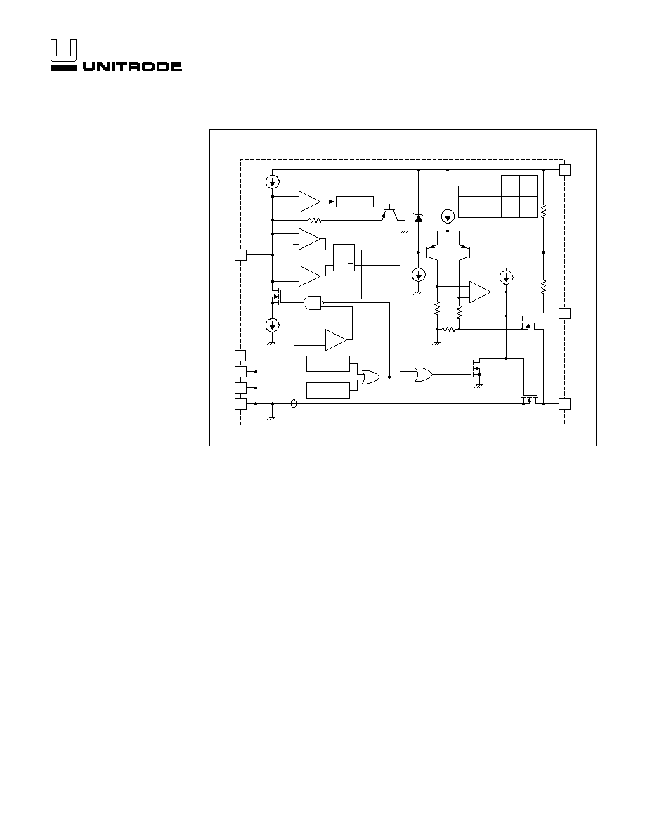
BLOCK DIAGRAM
UDG-99030
The UCC384 family of negative linear series pass regula-
tors is tailored for low drop out applications where low
quiescent
power
is
important.
Fabricated
with
a
BCDMOS technology ideally suited for low input to out-
put differential applications, the UCC384 will pass 0.5A
while requiring only 0.2V of input voltage headroom.
Drop out voltage decreases linearly with output current,
so that drop out at 50mA is less than 20mV.
Quiescent current consumption for the device under nor-
mal (non-drop out) conditions is typically 200
µA. An inte-
grated charge pump is internally enabled only when the
device is operating near drop out with low VIN. This
guarantees that the device will meet the drop out specifi-
cations even for maximum load current and a VIN of
≠3.2V with only a modest increase in quiescent current.
Quiescent current is always less than 350
µA, with the
charge pump enabled. Quiescent current of the UCC384
does not increase with load current.
Short circuit current is internally limited. The device re-
sponds to a sustained over current condition by turning
off after a T
ON
delay. The device then stays off for a pe-
riod, T
OFF
, that is 40 times the T
ON
delay. The device
then begins pulsing on and off at the T
ON/
T
OFF
duty cycle
of 2.5%. This drastically reduces the power dissipation
during short circuit such that heat sinking, if at all re-
quired, must only accommodate normal operation. An
external capacitor sets the on time. The off time is al-
ways 40 times T
ON
.
The UCC384 can be shutdown to 45
µA (maximum) by
pulling the SD/CT pin more positive than ≠0.6V. To allow
for simpler interfacing, the SD/CT pin may be pulled up
to +6V above the ground pin without turning on clamping
diodes.
Internal power dissipation is further controlled with ther-
mal overload protection circuitry. Thermal shutdown oc-
curs if the junction temperature exceeds 140∞C. The chip
will remain off until the temperature has dropped 20∞C.
DESCRIPTION
2
UCC284-5/-12/-ADJ
UCC384-5/-12/-ADJ
ELECTRICAL CHARACTERISTICS:
Unless otherwise specified, T
A
= 0∞C to 70∞C for the UCC384 and ≠40∞C to 85∞C
for the UCC284, VIN = VOUT ≠ 1.5V, I
OUT
= 0mA, C
OUT
= 4.7
µF, and CT = 0.015µF. For UCC384-ADJ, VOUT is set to ≠3.3V.
T
J
= T
A
.
PARAMETER
TEST CONDITIONS
MIN
TYP
MAX
UNITS
UCC384-5 Fixed ≠5V 0.5A Regulation Section
Output Voltage
T
A
= 25∞C
≠5.075
≠5
≠4.925
V
Over all conditions
≠5.100
≠4.850
V
Line Regulation
VIN = ≠5.3V to ≠15V
1.5
10
mV
Load Regulation
I
OUT
= 0mA to 0.5A
0.1
0.25
%
Output Noise Voltage
T
A
= 25∞C, BW = 10Hz to 10kHz
200
µVRMS
Drop Out Voltage, VOUT ≠ VIN
I
OUT
0.5A, VOUT = ≠4.8V
0.20
0.50
V
I
OUT
50mA, VOUT = ≠4.8V
20
50
mV
UCC384-5 Fixed ≠5V 0.5A Power Supply Section
Input Voltage Range
≠15
≠5.2
V
Quiescent Current Charge Pump On
VIN = ≠4.85V (Note 1)
280
350
µA
Quiescent Current
VIN = ≠15V
200
250
µA
Quiescent Current in Shutdown
VIN = ≠15V, SD/CT = 0V, No Load
24
45
µA
Shutdown Threshold
At Shutdown Pin
≠1.0
≠0.6
≠0.4
V
Shutdown Input Current
SD/CT = 0V
5
17
25
µA
Output Leakage in Shutdown
VIN = ≠15V, VOUT = 0, 25
∞C
1
10
A
Over Temperature
50
A
Over Temperature Shutdown
140
∞C
Over Temperature Hysteresis
20
∞C
UCC384-5 Fixed ≠5V 0.5A Current Limit Section
Peak Current Limit
VOUT = 0V
0.7
1.1
1.5
A
Over Current Threshold
0.55
0.7
0.9
A
Current Limit Duty Cycle
VOUT = 0V
2.5
4
%
Overcurrent Time Out, T
ON
VOUT = 0V
300
450
650
µs
UCC384-12 Fixed 12V 0.5A Regulation Section
Output Voltage
T
A
= 25∞C
≠12.18
≠12
≠11.82
V
Over all conditions
≠12.24
≠11.64
V
Line Regulation
VIN = ≠12.5V to ≠15V
5
15
mV
Load Regulation
I
OUT
= 0mA to 0.5A
0.1
0.3
%
Output Noise Voltage
T
A
= 25∞C, BW = 10Hz to 10kHz
200
µVRMS
Drop Out Voltage, VOUT - VIN
I
OUT
0.5A, VOUT = ≠11.6V
0.15
0.5
V
I
OUT
50mA, VOUT = ≠11.6V
15
50
mV
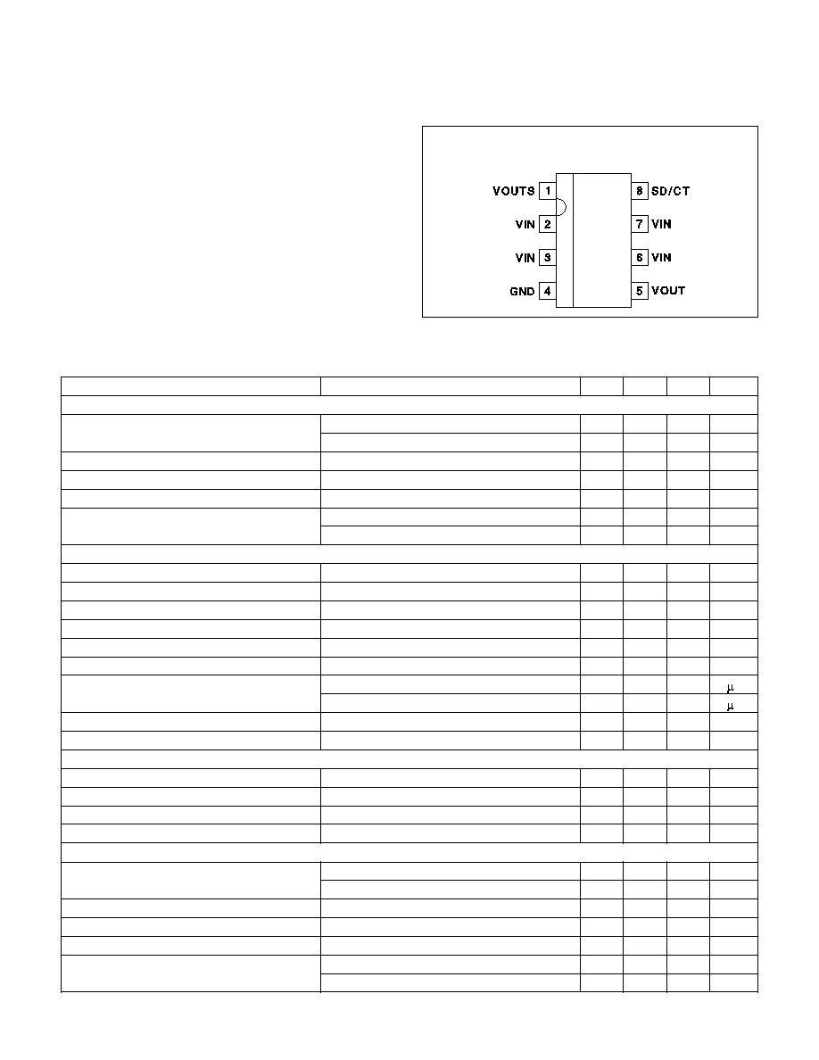
CONNECTION DIAGRAM
SOIC-8 (Top View)
DP Package
Supply Voltage, VIN . . . . . . . . . . . . . . . . . . . . . . . . . . . . . ≠16V
Shutdown Voltage, SD/CT . . . . . . . . . . . . . . . . . . . . +6V to ≠5V
Storage Temperature . . . . . . . . . . . . . . . . . . .
-65∞C to +150∞C
Junction Temperature . . . . . . . . . . . . . . . . . . . ≠55∞C to +150∞C
Lead Temperature (Soldering, 10 sec.) . . . . . . . . . . . . . +300∞C
All voltages are with respect to ground. Currents are positive
into, negative out of the specified terminal. All voltages are with
respect to ground. Consult Packaging Section of Databook for
thermal limitations and considerations of packages.
ABSOLUTE MAXIMUM RATINGS
3
UCC284-5/-12/-ADJ
UCC384-5/-12/-ADJ
ELECTRICAL CHARACTERISTICS:
Unless otherwise specified, T
A
= 0∞C to 70∞C for the UCC384 and ≠40∞C to 85∞C
for the UCC284, VIN = VOUT ≠ 1.5V, I
OUT
= 0mA, C
OUT
= 4.7
µF, and CT = 0.015µF. For UCC384-ADJ, VOUT is set to ≠3.3V.
T
J
= T
A
.
PARAMETER
TEST CONDITIONS
MIN
TYP
MAX
UNITS
UCC384-12 Fixed ≠12V 0.5A Power Supply Section
Input Voltage Range
≠15
≠12.2
V
Quiescent Current
VIN = ≠15V
220
350
µA
Quiescent Current in Shutdown
VIN = ≠15V, SD/CT = 0V, No Load
24
45
µA
Shutdown Threshold
At Shutdown Pin
≠1.0
≠0.6
≠0.4
V
Shutdown Input Current
SD/CT = 0V
5
17
25
µA
Output Leakage in Shutdown
VIN = ≠15V, VOUT = 0, 25
∞C
1
10
µA
Over Temperature
50
µA
Over Temperature Shutdown
140
∞C
Over Temperature Hysteresis
20
∞C
UCC384-12 Fixed -12V 0.5A Current Limit Section
Peak Current Limit
VOUT = 0V
0.7
1.2
1.5
A
Over Current Threshold
0.55
0.7
0.9
A
Current Limit Duty Cycle
VOUT = 0V
2.5
4
%
Over Current Time Out, T
ON
VOUT = 0V
300
450
650
µs
UCC384-ADJ Adjustable 0.5A Regulation Section
Reference Voltage
T
A
= 25∞C
≠1.27
≠1.25
≠1.23
V
Over Temperature
≠1.275
≠1.215
V
Line Regulation
VIN = ≠3.5V to ≠15V, VOUT = VOUTS
0.5
3
mV
Load Regulation
I
OUT
= 0mA to 0.5A
0.1
0.18
%
Output Noise Voltage
T
A
= 25∞C, BW = 10Hz to 10kHz
200
µVRMS
Drop Out Voltage, VOUT - VIN
I
OUT
0.5A, VOUT = ≠3.15V
0.25
0.5
V
I
OUT
50mA, VOUT = 3.15V
25
50
mV
Sense Pin Input Current
100
250
nA
UCC384-ADJ Adjustable 0.5A Power Supply Section
Input Voltage Range
≠15
≠3.5
V
Undervoltage Lockout
≠3.2
≠2.7
V
Quiescent Current Charge Pump On
VIN = ≠3.15V (Note 1)
200
350
µA
Quiescent Current
VIN = ≠15V
200
250
µA
Quiescent Current in Shutdown
VIN = ≠15V, SD/CT = 0V, No Load
24
45
µA
Shutdown Threshold
At Shutdown Pin
≠1.0
≠0.6
≠0.4
V
Shutdown Input Current
SD/CT = 0V
5
17
25
µA
Output Leakage in Shutdown
VIN = ≠15V, VOUT = 0, 25
∞C
1
10
µA
Over Temperature
50
µA
Over Temperature Shutdown
140
∞C
Over Temperature Hysteresis
20
∞C
UCC384-ADJ Adjustable 0.5A Current Limit Section
Peak Current Limit
VOUT = 0V
0.7
1.1
1.5
A
Over Current Threshold
0.55
0.7
0.9
A
Current Limit Duty Cycle
VOUT = 0V
2.5
4
%
Over Current Time Out, T
ON
VOUT = 0V
300
450
650
µs
Note 1: Internal Charge Pump is enabled only for drop-out condition with low VIN. Only in this condition is the Charge Pump re-
quired to provide additional output FET gate drive to maintain drop-out specifications. For conditions where the Charge
Pump is not required, it is disabled, which lowers overall device power consumption.

4
UCC284-5/-12/-ADJ
UCC384-5/-12/-ADJ
GND: This is the low noise ground reference input. All
voltages are measured with respect to the GND pin.
SD/CT: This is the shutdown pin and also the short cir-
cuit timing pin. Pulling this pin more positive than ≠0.6V
will put the circuit in a low current shutdown mode.
Placing a timing capacitor between this pin and GND will
set the short circuit charging time, TON during an
overcurrent condition. During an overcurrent condition,
the output will be pulsed at approximately a 2.5% duty
cycle.
Note: The CT capacitor must be connected between this pin
and GND, not VIN, to assure that the SD/CT pin is not pulled
significantly negative during power-up. This pin should not be
externally driven more negative than ≠5V or the device will be
damaged.
VIN: This is the negative input supply. Bypass this pin to
GND with at least 1
µF of low ESR, ESL capacitance.
VOUT: Regulated negative output voltage. A single
4.7
µF capacitor should be connected between this pin
and GND. Smaller value capacitors can be used for light
loads, but this will degrade the load step performance of
the regulator.
VOUTS: This is the feedback pin for sensing the output
of the regulator. For the UCC384-5 and UCC384-12 ver-
sions, VOUTS can be connected directly to VOUT. If the
load is placed at a considerable distance from the regu-
lator, the VOUTS lead can be used as a Kelvin connec-
tion
to
minimize
errors
due
to
lead
resistance.
Connecting VOUTS at the load will move the resistance
of the VOUT wire into the control loop of the regulator,
thereby effectively canceling the IR drop associated with
the load path.
When using a UCC384-ADJ, the output voltage can be
programmed by placing a resistor divider across the out-
put to GND. VOUTS is connected to the center tap of the
divider providing the feedback for the regulator. This con-
figuration is shown in Fig. 1.
PIN DESCRIPTIONS
Overview
The UCC384 family of NEGATIVE low dropout linear
(LDO) regulators provides a regulated output voltage for
applications with up to 0.5A of load current. The regula-
tors feature a low dropout voltage and short circuit pro-
tection,
making
their
use
ideal
for
demanding
applications requiring fault protection.
Programming the output voltage on the UCC384
The UCC384-5 and UCC384-12 have fixed output volt-
ages of ≠5V and ≠12V respectively. Connecting VOUTS
to VOUT will give the proper output voltage with respect
to ground.
The UCC384-ADJ can be programmed for any output
voltage between ≠1.25V and ≠15V. This is easily accom-
plished with the addition of an external resistor divider
connected between GND and VOUT with VOUTS con-
nected to the center tap of the divider. For an output of
≠1.25V, no resistors are needed and VOUTS is con-
nected directly to VOUT. The regulator input voltage can-
not be more positive than the UVLO threshold, or
approximately ≠3V. Thus, low drop out cannot be
achieved when programming the output voltage more
positive than approximately ≠3.3V. A typical Application
circuit is shown in Fig. 1.
For the UCC384-ADJ, the output voltage is programmed
by the following equation:
VOUT
R
R
= -
∑ +
1 25
1
1
2
.
(1)
When R1 or R2 are selected to be greater than about
100k
, a small ceramic capacitor should be placed
across R1 to cancel the input pole created by R1 and the
parasitic capacitance appearing on VOUTS. Values of
approximately 20pF should be adequate.
APPLICATION INFORMATION
5
4
1
3
2
R1
R2
VOUT
VOUTS
GND
6
7
VIN
VIN
VIN
VIN
CIN
VIN
8
CT
SD/CT
COUT
VOUT
+
+
(+)
(≠)
(+)
(≠)
C1
UCC384-ADJ
1
µF
4.7
µF
0.015
µF
Figure 1. Typical application schematic.
UDG-99029
Note 1: R1 and R2 for ≠ADJ version only. For ≠5 and ≠12
versions, connect VOUTS to VOUT.
5
UCC284-5/-12/-ADJ
UCC384-5/-12/-ADJ
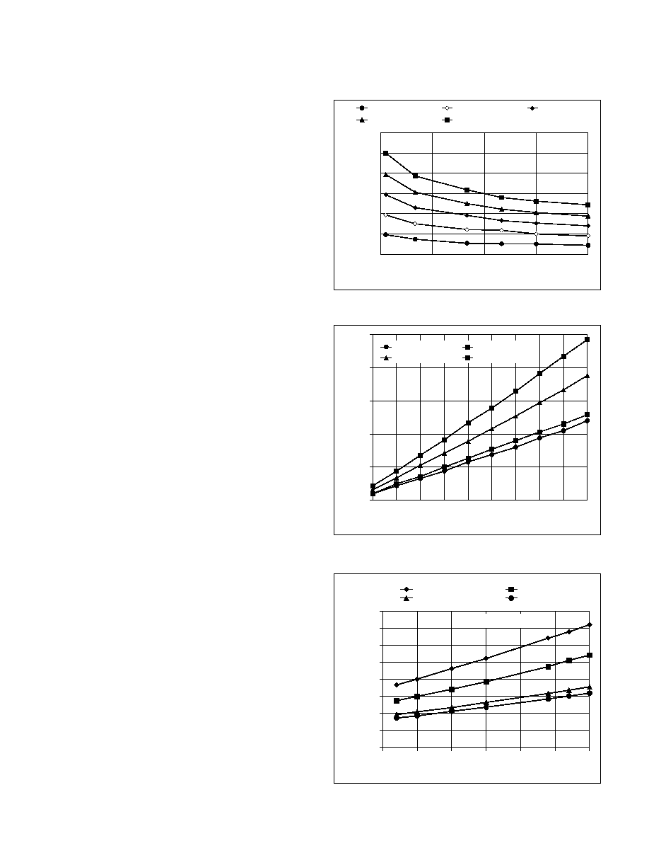
Dropout Performance
The UCC384 is tailored for low dropout applications
where low quiescent power is important. Fabricated with
a BCDMOS technology ideally suited for low input to out-
put differential applications, the UCC384 will pass 0.5A
while requiring only 0.2V of headroom. The dropout volt-
age is dependent on operating conditions such as load
current, input and load voltages, and temperature. The
UCC384 achieves a low R
DS
(on) through the use of an
internal charge-pump that drives the MOSFET gate.
Fig. 2 shows typical dropout voltages versus output volt-
age for the UCC384≠5V and ≠12V versions as well as
the UCC384-ADJ version programmed between ≠3.3V
and ≠15V. Since the dropout voltage is also affected by
output current, Fig. 3 shows typical dropout voltages vs.
load current for different values of V
OUT
.
Operating temperatures also effect the R
DS
(on) and the
dropout voltage of the UCC384. Fig. 4 shows typical
dropout voltages for the UCC384 over temperature un-
der a full load of 0.5A.
Short Circuit Protection
The UCC384 provides unique short circuit protection cir-
cuitry that reduces power dissipation during a fault.
When an overcurrent condition is detected, the device
enters a pulsed mode of operation, limiting the output to
a 2.5% duty cycle. This will reduce the heat sink require-
ments during a fault. The operation of the UCC384 dur-
ing an overcurrent condition is shown in Fig. 5.
UCC384 Short Circuit Timing
During normal operation the output voltage is in regula-
tion and the SD/CT pin is held to ≠1.5V via a 50k
inter-
nal source impedance. If the output current rises above
the Overcurrent Threshold, the CT capacitor will be
charged by a 40
µA current sink. The voltage on the
SD/CT pin will move in a negative direction with respect
to GND.
During an overcurrent condition, the regulator will ac-
tively limit the maximum output current to the Peak Cur-
rent Limit. This will limit the output voltage of the
regulator to:
V
I
R
OUT
PEAK
L
=
∑
If the output current stays above the Overcurrent Thresh-
old, the voltage on the SD/CT pin will reach ≠2.6V with
respect to GND and the output will turn off. The CT ca-
pacitor is then discharged by a 1
µA current source.
When the voltage on the SD/CT pin reaches ≠1.6V with
respect to GND, the output will turn back on. This pro-
cess will repeat until the output current falls below the
Overcurrent Threshold.
APPLICATION INFORMATION (cont.)
0
0.05
0.1
0.15
0.2
0.25
0.3
3
6
9
12
15
≠Vout (V)
V
i
n
-
V
out
(
V
)
Iout=0.1A
Iout=0.2A
Iout=0.3A
Iout=0.4A
Iout=0.5A
Figure 2. Dropout voltage vs. output voltage.
0
0.05
0.1
0.15
0.2
0.25
0.3
0.35
0.4
-50
-25
0
25
50
75
100
TEMPERATURE (∞C)
V
IN
-V
O
U
T
(
v
)
Vout = -3.3v
Vout = -5v
Vout = -12v
Vout = -15v
Iout = ≠500mA
Figure 4. Dropout voltage vs. temperature.
0
0.05
0.1
0.15
0.2
0.25
0.05 0.1 0.15 0.2 0.25 0.3 0.35 0.4 0.45 0.5
Iout (A)
V
i
n
-
V
out
(V
)
VOUT= -15V
VOUT= -12V
VOUT= -5V
VOUT= -3.3V
Figure 3. Dropout voltage vs. load current.

6
UCC284-5/-12/-ADJ
UCC384-5/-12/-ADJ
IOUT=0A
IOUT (NOM)
IOVER
IPEAK
VOUT = 0V
VOUT
=(IPEAK)(RL)
VOUT NOM. (≠V)
CT = 0V
CT (NOM) = ≠ 1.6V
CT = ≠ 2.6V
NOTE: CURRENT FLOW IS INTO THE DEVICE
~40xTON
~40xTON
T
ON
T
OFF
T
ON
T
OFF
T
ON
Figure 5. Short circuit timing.
APPLICATION INFORMATION (cont.)
UDG-99031
T
ON
, the time the output is on during an overcurrent con-
dition is determined by the following equation:
( )
T
CT
F
V
A
ON
=
∑
µ
µ
1
40
seconds
(2)
TOFF, the time the output is off during an overcurrent
condition is determined by the following equation:
( )
T
CT
F
V
A
OFF
=
∑
µ
µ
1
1
seconds
(3)
Capacitive Loads
A capacitive load on the regulator's output will appear as
a short circuit during start-up. If the capacitance is too
large, the output voltage will not come into regulation
during the initial TON period and the UCC384 will enter a
pulsed mode operation. For a constant current load the
maximum allowed output capacitance is calculated as
follows:
(
)
( )
( )
[
]
( )
( )
C
I
A
I
A
T
V
V
Farads
OUT
PEAK
LOAD
ON
OUT
max
sec
=
-
∑
(4)
7
UCC284-5/-12/-ADJ
UCC384-5/-12/-ADJ
For worst case calculations, the minimum value for TON
should be used, which is based on the value of CT ca-
pacitor selected. For a resistive load the maximum output
capacitor can be estimated as follows:
(
)
( )
( )
( )
C
T
R
n
V
V
I
A
R
OUT
ON
LOAD
OUT
MAX
LOAD
max
sec
( )
( )
=
∑
-
∑
l
1
1
Farads
(5)
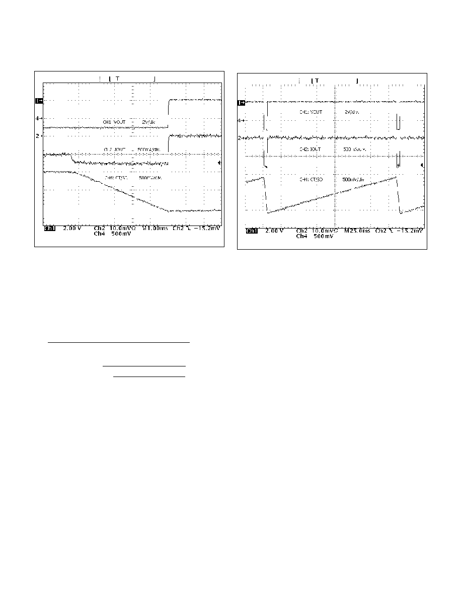
Fig. 6 and Fig. 7 are oscilloscope photos of the
UCC384-ADJ operating during an overcurrent condition.
Fig. 6 shows operation of the circuit as the output current
initially rises above the Overcurrent Threshold. This is
shown on a 1ms/div. scale. Fig. 7 shows operation of the
same circuit on a 25ms/div. scale allowing us to see one
complete cycle of operation during an overcurrent condi-
tion.
Shutdown Feature of the UCC384
The shutdown feature of the UCC384 allows the device
to be placed in a low quiescent current mode. The
UCC384 is shut down by pulling the SD/CT pin more
positive than ≠0.6V with respect to GND. Fig. 8 shows
how a shutdown circuit can be configured for the
UCC384 using a standard TTL signal to control it.
Controlling the SD/CT Pin
Forcing the SD/CT pin to any fixed voltage will affect the
operation of the circuit. As mentioned before, pulling the
SD/CT pin more positive than ≠0.6V will put the circuit in
a shutdown mode, limiting the quiescent current to less
than 45
µA. Pulling this pin more positive than +6V with
respect to GND will damage the device.
Forcing the SD/CT pin to any fixed voltage between
≠0.6V and ≠2.6V with respect to GND will cause the cir-
cuit to ignore an overcurrent condition. In this situation,
the output will not be pulsed at a 2.5% duty cycle, but the
output current will still be limited to the Peak Current
Limit. This circuit maybe used where a fixed current limit
is needed, while a 2.5% duty cycle is undesirable. The
UCC384 will supply a maximum current in this configura-
tion as long as the temperature of the device does not
exceed the Over Temperature Shutdown. This will be de-
termined by the Peak Current being supplied, the input
and output voltages, and the type of heat sink being
used. Thermal Design will be discussed later on in this
data sheet.
Forcing the SD/CT pin to a voltage level between ap-
proximately ≠2.6V and ≠5V with respect to GND will turn
the output off completely. The output will stay off as long
as the voltage is applied. Pulling this pin more negative
than ≠5V with respect to GND will damage the device.
APPLICATION INFORMATION (cont.)
Figure 6. UCC384-ADJ operation during overcurrent
condition (1ms/div).
Figure 7. UCC384-ADJ operation during overcurrent
condition (25ms/div.).
8
UCC284-5/-12/-ADJ
UCC384-5/-12/-ADJ
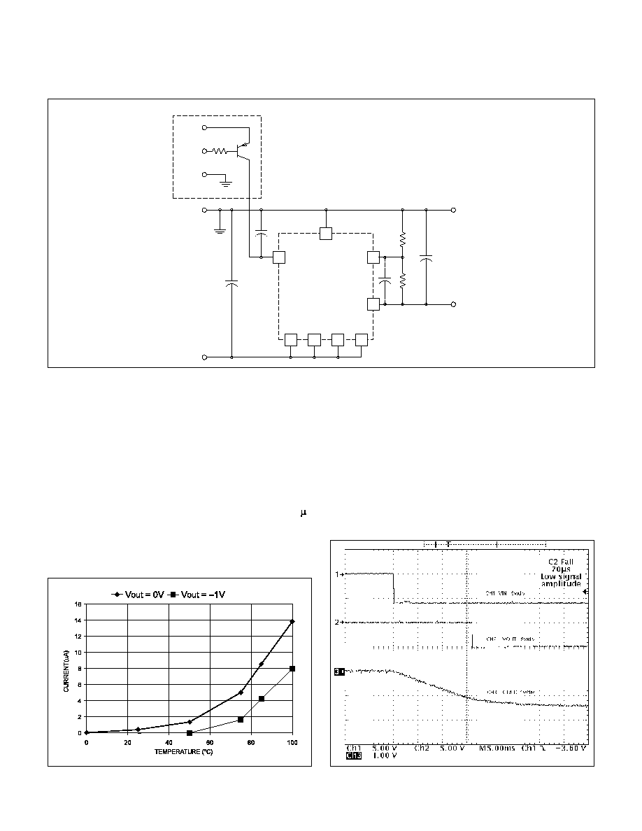
Fig. 9 shows typical VOUT leakage current as a function
of temperature during shutdown.
VIN to VOUT Delay
During power-up there is a delay between VIN and
VOUT. The majority of this delay time is due to the
charging time of the CT capacitor. When VIN moves
more negative than the UVLO of the device with respect
to GND, the CT capacitor will start to charge. A 17 A
current sink is used only during power-up to charge the
CT capacitor. When the voltage on the SD/CT pin
reaches approximately ≠1.6V with respect to GND, the
output will turn on and regulate. The larger the value of
the CT capacitor, the greater the delay time between VIN
and VOUT. Fig. 10 shows the VIN to VOUT startup de-
lay, approximately 16ms, for a circuit with CT = 0.22
µF.
Shorter delay times can be achieved with a smaller CT
capacitor. The problem with a smaller CT capacitor is
that with a very large load, the circuit may stay in
overcurrent mode and never turn on. A circuit with a
large capacitive load will need a large CT capacitor to
operate properly.
Figure 9. VOUT leakage current in shutdown (V
IN
=
≠15V).
5
4
1
3
2
R1
R2
VOUT
VOUTS
GND
6
7
VIN
VIN
VIN
VIN
CIN
VIN
8
CT
SD/CT
COUT
VOUT
+
+
(+)
(≠)
(+)
(-)
C1
UCC384-ADJ
TTL SHUTDOWN CIRCUIT
1
µF
0.015
µF
4.7
µF
470k
+5V
LOGIC
INPUT
+5V
GND
Figure 8. TTL controlled shutdown circuit for the UCC384.
APPLICATION INFORMATION (cont.)
UDG-99032
Figure 10. VIN to VOUT delay time during power-up
with CT = 0.22
µ
F.
9
UCC284-5/-12/-ADJ
UCC384-5/-12/-ADJ
One way to shorten the delay from VIN to VOUT during
power-up, is by the use of the Quick Start-up circuit
shown in Fig. 11.
With the Quick Start-Up circuit, the delay time between
VIN and VOUT during start-up can be reduced dramati-
cally. Fig. 12 shows that with the Quick Start-Up circuit,
the VIN to VOUT delay time has been reduced to ap-
proximately 1ms.
Operation of the Quick Start-Up Circuit
During normal start-up, the UCC384 will not turn on until
the voltage on the SD/CT pin reaches approximately
≠1.6V with respect to ground. It will take a certain
amount of time for the CT capacitor to charge to this
point. For a circuit that has a very large load, the CT ca-
pacitor will also need to be large in order for the
overcurrent timing to work properly. A large value of ca-
pacitance on the SD/CT pin will increase the VIN to
VOUT delay time.
The quick start-up circuit uses Q1 to quickly pull the
SD/CT pin in a negative direction during start-up, thus
decreasing the VIN to VOUT delay time. When VIN is ap-
plied to the circuit, Q1 turns on and starts to charge the
CT capacitor. The current pulled through R4 will deter-
mine the rate at which CT is charged. R4 can be calcu-
lated as follows:
( )
( )
( )
R
V
V
T
CT F
IN
D
4
1 6
=
∑
∑
sec
.
Ohms
(6)
TD is the approximate VIN to VOUT delay time you wish
to achieve.
Q1 will need to be turned off after a fixed time to prevent
the SD/CT pin from going too far negative with respect to
GND. If the SD/CT pin is allowed to go too far negative
with respect to GND, the output will turn off again or pos-
sibly even damage the SD/CT pin. The maximum
amount of time that Q1 should be allowed to be on is re-
ferred to as TM and can be calculated as follows:
T
T
M
D
=
∑
2 6
1 6
.
.
Seconds
(7)
APPLICATION INFORMATION (cont.)
5
4
1
3
2
R1
R2
VOUT
VOUTS
GND
6
7
VIN
VIN
VIN
VIN
CIN
VIN
8
CT
SD/CT
COUT
VOUT
+
+
(+)
(≠)
(+)
(≠)
C1
UCC384-ADJ
R3
C2
2N7000
QUICK START CURRENT
R4
0.22
µF
0.1
µF
18k
12k
1
µF
4.7
µF
Q1
Figure 11. Quick start-up circuit for UCC384.
UDG-99032
Figure 12. VIN to VOUT delay time with quick
start-up circuit.
10
UCC284-5/-12/-ADJ
UCC384-5/-12/-ADJ
R3 along with C2 set the time that Q1 is allowed to be
on. Since TM is the maximum amount of time that Q1
should be allowed to stay on, an added safety margin
may be to use 0.9
∑ TM instead. This will ensure that Q1
is turned off in the proper amount of time. With a chosen
value for C2, R3 can be calculated as follows:
( )
( )
( )
( )
R
T
C
F
n
V
V
V
V
M
IN
IN
3
0 9
2
1
1 6
=
∑
∑
∑ -
-
.
sec
.
l
Ohms
(8)
After the CT capacitor has charged up for a time equal to
0.9
∑ TM , Q1 will turn off and allow the SD/CT pin to be
pulled back to ≠1.5V with respect to GND through a 50k
resistor. At this point , the SD/CT pin can be used by the
UCC384 overcurrent timing control.
Minimum V
IN
To V
OUT
Delay Time
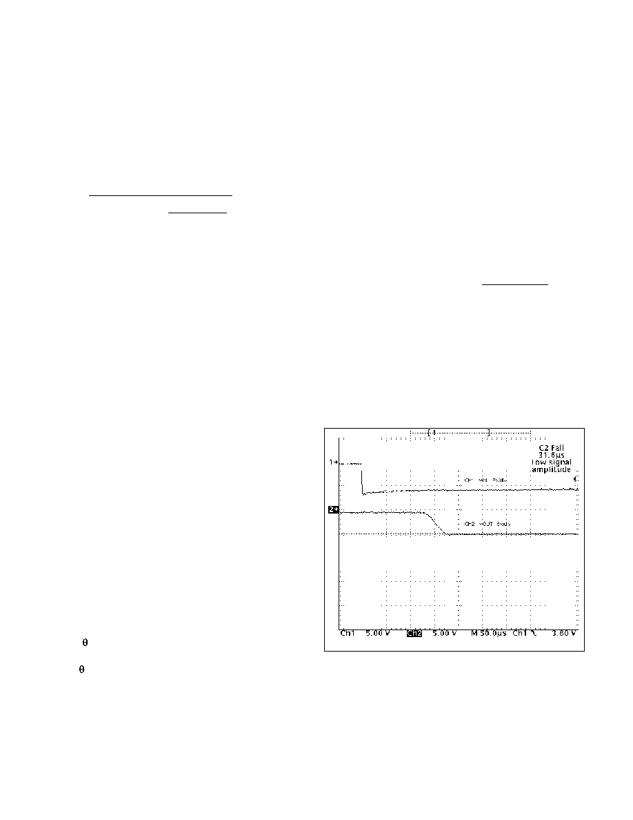
Although it may desirable to have as short a delay time
as possible, a small portion of this delay time is fixed by
the UCC384 and cannot be shortened. This is shown in
Fig. 13, where the CT capacitor has been removed from
the circuit completely, giving a fixed VIN to VOUT delay
of approximately 150
µs for a circuit with VIN = ≠6V and
VOUT = ≠5V.
Thermal Design
The Packaging Information section of this data book con-
tains reference material for the thermal ratings of various
packages. The section also includes an excellent article
entitled
Thermal Characteristics of Surface Mount Pack-
ages
, which is the basis for the following discussion.
Thermal design for the UCC384 includes two modes of
operation, normal and pulsed. In normal mode, the linear
regulator and heat sink must dissipate power equal to
the maximum forward voltage drop multiplied by the
maximum load current. Assuming a constant current
load, the expected heat rise at the regulator's junction
can be calculated as follows:
(
)
T
P
jc
ca
C
RISE
DISS
=
∑
+
∞
(9)
Theta ( ) is the thermal resistance and P
DISS
is the
power dissipated. The junction to case thermal resis-
tance (
jc
) of the SOIC-8 DP package is 22∞C/W. In or-
der to prevent the regulator from going into thermal
shutdown, the case to ambient thermal resistance (
ja
)
must keep the junction temperature below 150
∞C. If the
UCC384 is mounted on a 5 square inch pad of 1 ounce
copper, for example, the thermal resistance (
ja
) be-
comes 40-70
∞C/W. If a lower thermal resistance is re-
quired by the application, the device heat sinking would
need to be improved.
When the UCC384 is in a pulsed mode, due to an
overcurrent condition, the maximum average power dis-
sipation is calculated as follows:
( )
( )
[
]
( )
( )
( )
P
V
V
V
V
I
A
T
T
Watt
AVE
IN
OUT
PEAK
ON
ON
=
-
∑
∑
∑
sec
sec
40
s
(10)
As seen in equation 10, the average power during a fault
is reduced dramatically by the duty cycle, allowing the
heat sink to be sized for normal operation. Although the
peak power in the regulator during the T
ON
period can be
significant, the thermal mass of the package will gener-
ally keep the junction temperature from rising unless the
T
ON
period is increased to several milliseconds.
APPLICATION INFORMATION (cont.)
Figure 13. VIN to VOUT delay with CT capacitor
removed.
UNITRODE CORPORATION
7 CONTINENTAL BLVD. ∑ MERRIMACK, NH 03054
TEL. (603) 424-2410 FAX (603) 424-3460