
UCC284Ù5, UCC284Ù12, UCC284ÙADJ, UCC384Ù5, UCC384Ù12, UCC384ÙADJ
LOW-DROPOUT 0.5-A NEGATIVE LINEAR REGULATOR
SLUS234D Ù JANUARY 2000 Ù REVISED FEBRUARY 2002
1
POST OFFICE BOX 655303
ñ
DALLAS, TEXAS 75265
D
Precision Negative Series Pass Voltage
Regulation
D
0.2 V Dropout at 0.5 A
D
Wide Input Voltage Range Ù3.2 V to Ù15 V
D
Low Quiescent Current Irrespective of Load
D
Simple Logic Shutdown Interfacing
D
Ù5 V, Ù12 V, and Adjustable Output
D
2.5% Duty Cycle Short Circuit Protection
description
The UCC384-x family of negative linear-series pass regulators is tailored for low-dropout applications where
low-quiescent power is important. Fabricated with a BCDMOS technology ideally suited for low input-to-output
differential applications, the UCC384-x passes 0.5 A while requiring only 0.2 V of input-voltage headroom.
Dropout voltage decreases linearly with output current, so that dropout at 50 mA is less than 20 mV.
Quiescent current consumption for the device under normal (non-dropout) conditions is typically 200
ç
A. An
integrated charge pump is internally enabled only when the device is operating near dropout with low VIN. This
ensured that the device meets the dropout specifications even for maximum load current and a VIN of Ù3.2 V
with only a modest increase in quiescent current. Quiescent current is always less than 350
ç
A, with the charge
pump enabled. The quiescent current of the UCC384 does not increase with load current.
Short-circuit current is internally limited. The device responds to a sustained overcurrent condition by turning
off after a t
ON
delay. The device then stays off for a period, t
OFF
, that is 40 times the t
ON
delay. The device then
begins pulsing on and off at the t
ON
/t
OFF
duty cycle of 2.5%. This drastically reduces the power dissipation during
short circuit such that heat sinking, if at all required, must only accommodate normal operation. An external
capacitor sets the on time. The off time is always 40 times t
ON
.
The UCCx84-x can be shutdown to 45
ç
A (maximum) by pulling the SD/CT pin more positive than Ù0.7 V. To
allow for simpler interfacing, the SD/CT pin may be pulled up to 6 V above the ground pin without turning on
clamping diodes.
Internal power dissipation is further controlled with thermal-overload protection circuitry. Thermal shutdown
occurs if the junction temperature exceeds 140
¯
C. The chip remains off until the temperature has dropped 20
¯
C
(T
J
= 120
¯
C).
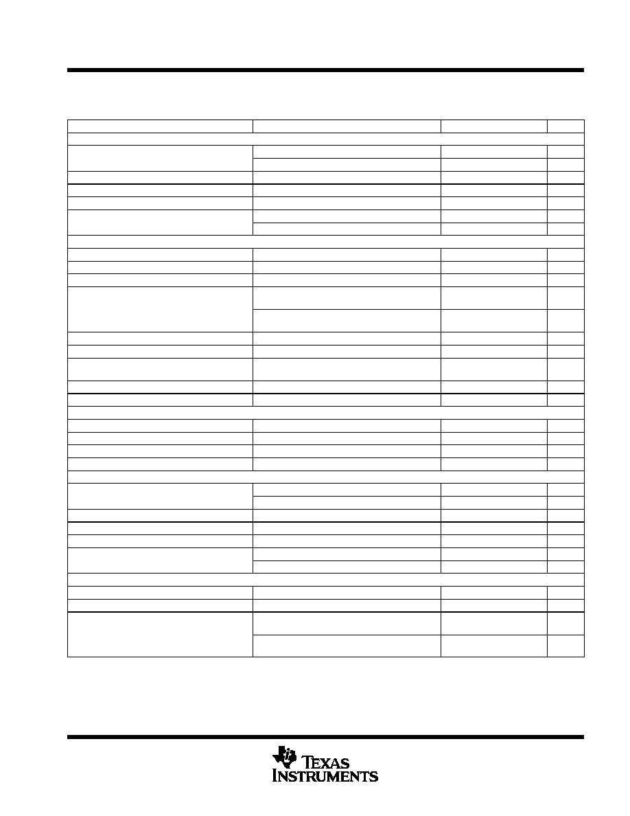
AVAILABLE OPTIONS
TA
OUTPUT VOLTAGE (V)
PACKAGE DEVICES
TA
TYP
(SOIC) DP
Ù5
UCC284DPÙ5
Ù 40
¯
C to 85
¯
C
Ù12
UCC284DPÙ12
40 C to 85 C
ADJ
UCC284DPÙADJ
Ù5
UCC384DPÙ5
0
¯
C to 70
¯
C
Ù12
UCC384DPÙ12
ADJ
UCC384DPÙADJ
All package types are available taped and reeled. Add TR suffix to device type
(e.g. UCC284DPÙ5TR) to order quantities of 3000 devices per reel.
Copyright
2000, Texas Instruments Incorporated
PRODUCTION DATA information is current as of publication date.
Products conform to specifications per the terms of Texas Instruments
standard warranty. Production processing does not necessarily include
testing of all parameters.
Please be aware that an important notice concerning availability, standard warranty, and use in critical applications of
Texas Instruments semiconductor products and disclaimers thereto appears at the end of this data sheet.
DP PACKAGE
(FRONT VIEW)
VIN
VIN
SD/CT
VOUT
VIN
VOUTS
VIN
GND
1
2
3
4
8
7
6
5

UCC284Ù5, UCC284Ù12, UCC284ÙADJ, UCC384Ù5, UCC384Ù12, UCC384ÙADJ
LOW-DROPOUT 0.5-A NEGATIVE LINEAR REGULATOR
SLUS234D Ù JANUARY 2000 Ù REVISED FEBRUARY 2002
2
POST OFFICE BOX 655303
ñ
DALLAS, TEXAS 75265
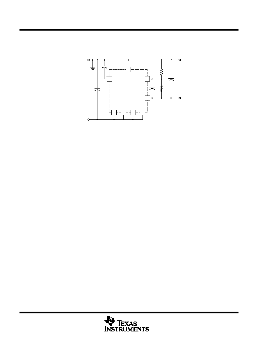
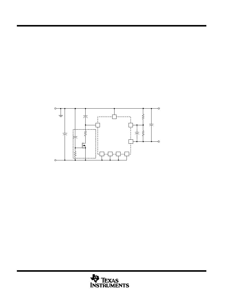
functional block diagram
3
8
2
6
7
5
R1
R2
1
4
GND
VOUTS
VOUT
1.25 V
Ù2.6 V
Ù1.6 V
OVERCURRENT
S
Q
Q
R
THERMAL
SHUTDOWN
1Ù
ç
A
DISCHARGE
40
ç
A
VPUMP
SD/CT
CHARGE
700 mA
50 k
GM
TON
TOFF
UVLO
VIN
VIN
VIN
VIN
Ù2.2 V
R1
R2
0
OPEN
UCC384ÙADJ
UCC384Ù5
UCC384Ù12
375K
375K
125K
43.6K
SHUTDOWN
Ù0.7 V
(Ù)
(+)
+
+
+
+
+
(Ù)
UDGÙ99030
absolute maximum ratings over operating free-air temperature (unless otherwise noted)
}
Input voltage range
, V
IN
Ù16 V
. . . . . . . . . . . . . . . . . . . . . . . . . . . . . . . . . . . . . . . . . . . . . . . . . . . . . . . . . . . . . . . . . .
Shutdown voltage range, SD/CT
Ù5 V to 6 V
. . . . . . . . . . . . . . . . . . . . . . . . . . . . . . . . . . . . . . . . . . . . . . . . . . . . . . .
Operating virtual junction temperature range, T
J
Ù55
¯
C to 150
¯
C
. . . . . . . . . . . . . . . . . . . . . . . . . . . . . . . . . . . . .
Storage temperature range T
stg
Ù65
¯
C to 150
¯
C
. . . . . . . . . . . . . . . . . . . . . . . . . . . . . . . . . . . . . . . . . . . . . . . . . . . .
Lead temperature (Soldering, 10 seconds)
300
¯
C
. . . . . . . . . . . . . . . . . . . . . . . . . . . . . . . . . . . . . . . . . . . . . . . . . .
Stresses beyond those listed under "absolute maximum ratings" may cause permanent damage to the device. These are stress ratings only, and
functional operation of the device at these or any other conditions beyond those indicated under "recommended operating conditions" is not
implied. Exposure to absolute-maximum-rated conditions for extended periods may affect device reliability.
All voltages are with respect to ground. Currents are positive into and negative out of the specified terminals.
UCC284Ù5, UCC284Ù12, UCC284ÙADJ, UCC384Ù5, UCC384Ù12, UCC384ÙADJ
LOW-DROPOUT 0.5-A NEGATIVE LINEAR REGULATOR
SLUS234D Ù JANUARY 2000 Ù REVISED FEBRUARY 2002
3
POST OFFICE BOX 655303
ñ
DALLAS, TEXAS 75265
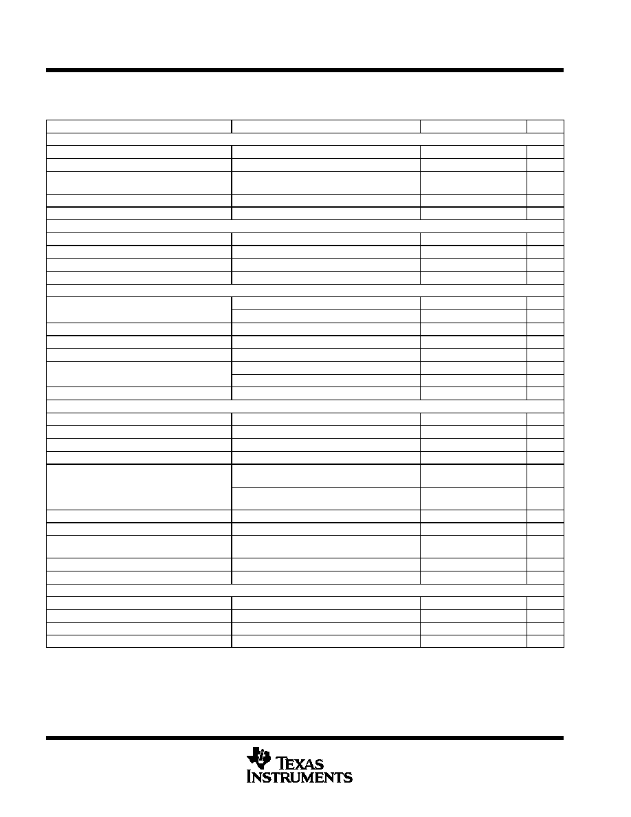
electrical characteristics T
A
= 0
¯
C to 70
¯
C for the UCC384 and Ù40
¯
C to 85
¯
C for the UCC284,
VIN = VOUT Ù 1.5 V, I
OUT
= 0 mA, C
OUT
= 4.7
ç
F, and CT = 0.015
ç
F. For UCC384ÙADJ, VOUT is set
to Ù3.3V (unless otherwise noted)
PARAMETER
TEST CONDITIONS
MIN
TYP
MAX
UNIT
UCC384Ù5 Fixed Ù5-V 0.5-A Regulation Section
Output voltage
TA = 25
¯
C
Ù5.075
Ù5
Ù4.925
V
Output voltage
Over all conditions
Ù5.100
Ù4.850
V
Line regulation
VIN = Ù5.2 V to Ù15 V
1.5
10
mV
Load regulation
IOUT = 0 mA to 0.5 A
0.1
0.25
%
Output noise voltage
TA = 25
¯
C,
BW = 10 Hz to 10 kHz
200
ç
VRMS
Dropout voltage VOUT
VIN
IOUT 0.5 A,
VOUT = Ù4.8 V
0.20
0.50
V
Dropout voltage, VOUT Ù VIN
IOUT 50 mA,
VOUT = Ù4.8 V
20
50
mV
UCC384Ù5 Fixed Ù5-V 0.5-A Power Supply Section
Input voltage range
Ù15
Ù5.2
V
Quiescent current charge pump on
VIN = Ù4.85 V,
See Note 1
280
350
ç
A
Quiescent current
VIN = Ù15 V
200
250
ç
A
Quiescent current in shutdown
VIN = Ù13 V,
SD/CT = 0 V
TA = 0
¯
C to 85
¯
C,
See Note 2
15
45
ç
A
Quiescent current in shutdown
VIN = Ù13 V,
SD/CT = 0 V
TA = Ù40
¯
C to 0
¯
C, See Note 2
100
ç
A
Shutdown threshold
At shutdown pin (SD/CT)
Ù1.0
Ù0.7
Ù0.4
V
Shutdown input current
SD/CT = 0 V
5
10
25
ç
A
Output leakage in shutdown
VIN = Ù15 V,
VOUT = 0 V,
See Note 3
1
50
ç
A
Overtemperature shutdown
140
¯
C
Overtemperature hysteresis
20
¯
C
UCC384Ù5 Fixed Ù5-V 0.5-A Current Limit Section
Peak current limit
VOUT = 0 V
0.7
1.1
1.5
A
Overcurrent threshold
0.55
0.7
0.9
A
Current limit duty cycle
VOUT = 0 V
2.5
4
%
Overcurrent time out, tON
VOUT = 0 V
300
500
700
ç
s
UCC384Ù12 Fixed 12-V 0.5-A Regulation Section
Output voltage
TA = 25
¯
C
Ù12.18
Ù12
Ù11.82
V
Output voltage
Over all conditions
Ù12.24
Ù11.64
V
Line regulation
VIN = Ù12.5 V to Ù15 V
5
15
mV
Load regulation
IOUT= 0 mA to 0.5 A
0.1
0.3
%
Output noise voltage
TA = 25
¯
C
BW = 10 Hz to 10 kHz
200
ç
VRMS
Dropout voltage VOUT
VIN
IOUT 0.5 A,
VOUT = Ù11.6 V
0.15
0.5
V
Dropout voltage, VOUT Ù VIN
IOUT 50 mA,
VOUT = Ù11.6 V
15
50
mV
UCC384Ù12 Fixed Ù12 V-0.5-A Power Supply Section
Input voltage range
Ù15
Ù12.5
V
Quiescent current
VIN = Ù15 V
220
350
ç
A
Quiescent current in shutdown
VIN = Ù13 V,
SD/CT = 0 V
TA = 0
¯
C to 85
¯
C,
See Note 2
15
45
ç
A
Quiescent current in shutdown
VIN = Ù13 V,
SD/CT = 0 V
TA = Ù40
¯
C to 0
¯
C, See Note 2
100
ç
A
NOTES:
1. The internal charge pump is enabled only for dropout condition with low VIN. Only in this condition is the charge pump required to
provide additional output FET fate drive to maintain dropout specifications. For conditions where the charge pump is not required,
it is disabled, which lowers overall device power consumption.
2. Ensured by design. Not production tested.
3. In the application during shutdown mode, output leakage current adds to quiescent current.
UCC284Ù5, UCC284Ù12, UCC284ÙADJ, UCC384Ù5, UCC384Ù12, UCC384ÙADJ
LOW-DROPOUT 0.5-A NEGATIVE LINEAR REGULATOR
SLUS234D Ù JANUARY 2000 Ù REVISED FEBRUARY 2002
4
POST OFFICE BOX 655303
ñ
DALLAS, TEXAS 75265
electrical characteristics T
A
= 0
¯
C to 70
¯
C for the UCC384 and Ù40
¯
C to 85
¯
C for the UCC284,
VIN = VOUT Ù 1.5 V, I
OUT
= 0 mA, C
OUT
= 4.7
ç
F, and CT = 0.015
ç
F. For UCC384ÙADJ, VOUT is set
to Ù3.3V (unless otherwise noted)
PARAMETER
TEST CONDITIONS
MIN
TYP
MAX
UNIT
UCC384Ù12 Fixed Ù12 V-0.5-A Power Supply Section (continued)
Shutdown threshold
At shutdown pin (SD/CT)
Ù1.0
Ù0.7
Ù0.4
V
Shutdown input current
SD/CT = 0 V
5
10
25
ç
A
Output leakage in shutdown
VIN = Ù15 V,
VOUT = 0 V,
See Note 3
1
50
ç
A
Overtemperature shutdown
140
¯
C
Overtemperature hysteresis
20
¯
C
UCC384Ù12 Fixed Ù12-V 0.5-A Current Limit Section
Peak current limit
VOUT = 0 V
0.7
1.1
1.5
A
Overcurrent threshold
0.55
0.7
0.9
A
Current limit duty cycle
VOUT = 0 V
2.5
4
%
Overcurrent time out, tON
VOUT = 0 V
300
500
700
ç
s
UCC384ÙADJ Adjustable 0.5-A Regulation Section
Reference voltage
TA = 25
¯
C
Ù1.27
Ù1.25
Ù1.23
V
Reference voltage
Over temperature
Ù1.275
Ù1.215
V
Line regulation
VIN = Ù3.5 V to Ù15 V,
VOUT = VOUTS
0.5
3
mV
Load regulation
IOUT = 0 mA to 0.5 A
0.1
0.18
%
Output noise voltage
BW = 10 Hz to 10 kHz,
TA = 25
¯
C
200
ç
VRMS
Dropout voltage VOUT
VIN
IOUT 0.5 A,
VOUT = Ù3.15 V
0.25
0.5
V
Dropout voltage, VOUT Ù VIN
IOUT 50 mA,
VOUT = Ù3.15 V
25
50
mV
Sense pin input current
100
250
nA
UCC384ÙADJ Adjustable 0.5-A Power Supply Section
Input voltage range
Ù15
Ù3.5
V
Undervoltage lockout
Ù3.2
Ù2.95
Ù2.7
V
Quiescent current charge pump on
VIN = Ù3.15 V,
See Note 1
200
350
ç
A
Quiescent current
VIN = Ù15 V
200
250
ç
A
Quiescent current in shutdown
VIN = Ù13 V,
SD/CT = 0 V
TA = 0
¯
C to 85
¯
C,
See Note 2
15
45
ç
A
Quiescent current in shutdown
VIN = Ù13 V,
SD/CT = 0 V
TA = Ù40
¯
C to 0
¯
C, See Note 2
100
ç
A
Shutdown threshold
At shutdown pin (SD/CT)
Ù1.0
Ù0.7
Ù0.4
V
Shutdown input current
SD/CT = 0V
5
10
25
ç
A
Output leakage in shutdown
VIN = Ù15V,
VOUT = 0 V,
See Note 3
1
50
ç
A
Overtemperature shutdown
140
¯
C
Overtemperature hysteresis
20
¯
C
UCC384ÙADJ Adjustable 0.5-A Current Limit Section
Peak current limit
VOUT = 0 V
0.7
1.1
1.5
A
Overcurrent threshold
0.55
0.7
0.9
A
Current limit duty cycle
VOUT = 0 V
2.5
4
%
Overcurrent time out, tON
VOUT = 0 V
300
500
700
ç
s
NOTES:
1. The internal charge pump is enabled only for dropout condition with low VIN. Only in this condition is the charge pump required to
provide additional output FET fate drive to maintain dropout specifications. For conditions where the charge pump is not required,
it is disabled, which lowers overall device power consumption.
2. Ensured by design. Not production tested.
3. In the application during shutdown mode, output leakage current adds to quiescent current.
UCC284Ù5, UCC284Ù12, UCC284ÙADJ, UCC384Ù5, UCC384Ù12, UCC384ÙADJ
LOW-DROPOUT 0.5-A NEGATIVE LINEAR REGULATOR
SLUS234D Ù JANUARY 2000 Ù REVISED FEBRUARY 2002
5
POST OFFICE BOX 655303
ñ
DALLAS, TEXAS 75265
pin descriptions
GND: This is the low noise ground reference input. All voltages are measured with respect to the GND pin.
SD/CT: This is the shutdown pin and also the short-circuit timing pin. Pulling this pin more positive than Ù0.7 V
puts the circuit in a low-current shutdown mode. Placing a timing capacitor between this pin and GND sets the
short-circuit charging time, t
ON
during an overcurrent condition. During an overcurrent condition, the output
pulses at approximately a 2.5% duty cycle.
NOTE:The CT capacitor must be connected between this pin and GND, not VIN, to assure that the
SD/CT pin is not pulled significantly negative during power-up. This pin should not be externally
driven more negative than Ù5 V or the device will be damaged.
VIN: This is the negative input supply. Bypass this pin to GND with at least 1
ç
F of low ESR or ESL capacitance.
VOUT: Regulated negative-output voltage. A single 4.7-
ç
F capacitor should be connected between this pin and
GND. Smaller value capacitors can be used for light loads, but this degrades the load-step performance of the
regulator.
VOUTS: This is the feedback pin for sensing the output of the regulator. For the UCC384-5 and UCC384-12
versions, VOUTS can be connected directly to VOUT. If the load is placed at a considerable distance from the
regulator, the VOUTS lead can be used as a Kelvin connection to minimize errors due to lead resistance.
Connecting VOUTS at the load moves the resistance of the VOUT wire into the control loop of the regulator,
thereby effectively canceling the IR drop associated with the load path.
APPLICATION INFORMATION
overview
The UCCx84-x family of negative low-dropout linear (LDO) regulators provides a regulated-output voltage for
applications with up to 0.5 A of load current. The regulators feature a low-dropout voltage and short-circuit
protection, making their use ideal for demanding applications requiring fault protection.
programming the output voltage on the UCC384
The UCC384-5 and UCC384-12 have output voltages that are fixed at Ù5 V and Ù12 V respectively. Connecting
VOUTS to VOUT gives the proper output voltage with respect to ground.
The UCC384-ADJ can be programmed for any output voltage between Ù1.25 V and Ù15 V. This is easily
accomplished with the addition of an external resistor divider connected between GND and VOUT with VOUTS
connected to the center tap of the divider. For an output of Ù1.25 V, no resistors are needed and VOUTS is
connected directly to VOUT. The regulator-input voltage cannot be more positive than the UVLO threshold, or
approximately Ù3 V. Thus, low dropout cannot be achieved when programming the output voltage more positive
than approximately Ù3.3 V. A typical application circuit is shown in Figure 1.
UCC284Ù5, UCC284Ù12, UCC284ÙADJ, UCC384Ù5, UCC384Ù12, UCC384ÙADJ
LOW-DROPOUT 0.5-A NEGATIVE LINEAR REGULATOR
SLUS234D Ù JANUARY 2000 Ù REVISED FEBRUARY 2002
6
POST OFFICE BOX 655303
ñ
DALLAS, TEXAS 75265
APPLICATION INFORMATION
programming the output voltage on the UCC384 (continued)
UDGÙ99029
5
4
1
3
2
R1
R2
VOUT
VOUTS
GND
6
7
VIN
VIN
VIN
VIN
CIN
VIN
8
CT
SD/CT
COUT
VOUT
+
+
(+)
(Ù)
(+)
(Ù)
C1
UCC384ÙADJ
1
ç
F
4.7
ç
F
0.015
ç
F
Figure 1. Typical Application Circuit
For the UCC384ÙADJ, the output voltage is programmed by the following equation:
VOUT
+ *
1.25
1
)
R1
R2
(1)
When R1 or R2 are selected to be greater than about 100 k
, a small ceramic capacitor should be placed across
R1 to cancel the input pole created by R1 and the parasitic capacitance appearing on VOUTS. Values of
approximately 20 pF should be adequate.
dropout performance
The UCC384 is tailored for low-dropout applications where low-quiescent power is important. Fabricated with
a BCDMOS technology ideally suited for low input-to-output differential applications, the UCC384 passes 0.5 A
while requiring only 0.2 V of headroom. The dropout voltage is dependent on operating conditions such as load
current, input and load voltages, and temperature. The UCC384 achieves a low R
DS
(on) through the use of an
internal charge-pump that drives the MOSFET gate.
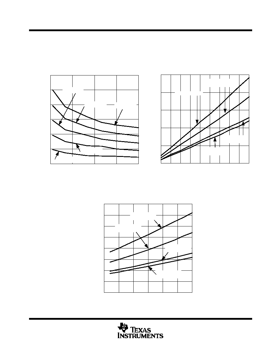
Figure 2 shows typical dropout voltages versus output voltage for the UCC384-5 V and -12 V versions as well
as the UCC384ÙADJ version programmed between Ù3.3 V and Ù15 V. Since the dropout voltage is also affected
by output current, Figure 3 shows typical dropout voltages versus load current for different values of VOUT.
Operating temperatures also affect the R
DS
(on) and the dropout voltage of the UCC384. Figure 4 shows typical
dropout voltages for the UCC384 over temperature under a full load of 0.5 A.
short-circuit protection
The UCC384 provides unique short-circuit protection circuitry that reduces power dissipation during a fault.
When an overcurrent condition is detected, the device enters a pulsed mode of operation, limiting the output
to a 2.5% duty cycle. This reduces the heat sink requirements during a fault. The operation of the UCC384 during
an overcurrent condition is shown in Figure 5.
UCC284Ù5, UCC284Ù12, UCC284ÙADJ, UCC384Ù5, UCC384Ù12, UCC384ÙADJ
LOW-DROPOUT 0.5-A NEGATIVE LINEAR REGULATOR
SLUS234D Ù JANUARY 2000 Ù REVISED FEBRUARY 2002
7
POST OFFICE BOX 655303
ñ
DALLAS, TEXAS 75265
APPLICATION INFORMATION
short-circuit protection (continued)
Figure 2
I
OUT
= 0.1 A
I
OUT
= 0.2 A
I
OUT
= 0.3 A
I
OUT
= 0.4 A
I
OUT
= 0.5 A
3
0.00
6
9
12
15
0.05
0.10
0.15
0.20
0.25
0.30
V
OUT
Ù Output Voltage Ù V
(V
IN
Ù
V
OUT
)
Ù
Dropout V
oltage
Ù
V
DROPOUT VOLTAGE
vs
OUTPUT VOLTAGE
Figure 3
V
OUT
= Ù15 V
V
OUT
= Ù12 V
V
OUT
= Ù5 V
0.05
0.05
0.15
0.10
0.25
0.35
0.45
0.15
0.20
0.25
I
OUT
Ù Load Current Ù A
DROPOUT VOLTAGE
vs
LOAD CURRENT
(V
IN
Ù
V
OUT
)
Ù
Dropout V
oltage
Ù
V
V
OUT
= Ù3.3 V
Figure 4
DROPOUT VOLTAGE
vs
TEMPERATURE
(V
IN
Ù
V
OUT
)
Ù
Dropout V
oltage
Ù
V
V
OUT
= Ù3.3 V
V
OUT
= Ù5 V
V
OUT
= Ù15 V
V
OUT
= Ù12 V
Ù50
Ù25
0
50
75
25
100
0.05
0.10
0
0.20
0.25
0.15
0.35
0.40
0.30
T
A
Ù Free-Air Temperature Ù
_
C

UCC284Ù5, UCC284Ù12, UCC284ÙADJ, UCC384Ù5, UCC384Ù12, UCC384ÙADJ
LOW-DROPOUT 0.5-A NEGATIVE LINEAR REGULATOR
SLUS234D Ù JANUARY 2000 Ù REVISED FEBRUARY 2002
8
POST OFFICE BOX 655303
ñ
DALLAS, TEXAS 75265
APPLICATION INFORMATION
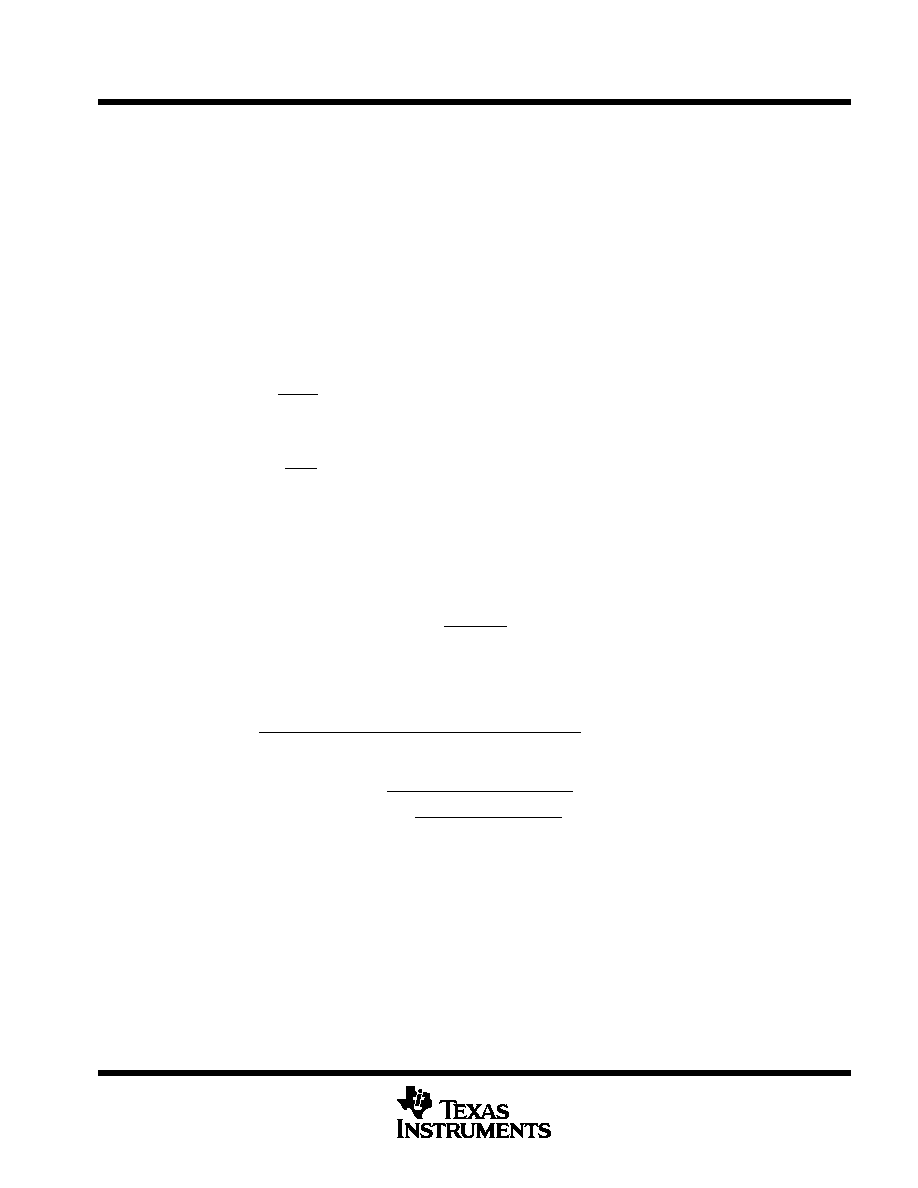
IOUT=0A
IOUT (NOM)
IOVER
IPEAK
VOUT = 0V
VOUT
=(IPEAK)(RL)
VOUT NOM. (ÙV)
CT = 0V
CT (NOM) = Ù 1.6V
CT = Ù 2.6V
NOTE: CURRENT FLOW IS INTO THE DEVICE
t ON
t OFF
t ON
t OFF
t ON
UDGÙ99031
~40 x tON
~40 x tON
Figure 5. Short Circuit Timing
UCC384 short circuit timing
During normal operation the output voltage is in regulation and the SD/CT pin is held to Ù1.5 V via a 50-k
internal-source impedance. If the output-current rises above the overcurrent threshold, the CT capacitor is
charged by a 40-
ç
A current sink. The voltage on the SD/CT pin moves in a negative direction with respect to
GND.
UCC284Ù5, UCC284Ù12, UCC284ÙADJ, UCC384Ù5, UCC384Ù12, UCC384ÙADJ
LOW-DROPOUT 0.5-A NEGATIVE LINEAR REGULATOR
SLUS234D Ù JANUARY 2000 Ù REVISED FEBRUARY 2002
9
POST OFFICE BOX 655303
ñ
DALLAS, TEXAS 75265
APPLICATION INFORMATION
UCC384 short-circuit timing (continued)
During an overcurrent condition, the regulator actively limits the maximum output current to the peak-current
limit. This limits the output voltage of the regulator to:
V
OUT
+
I
PEAK
R
L
(1)
If the output current stays above the overcurrent threshold, the voltage on the SD/CT pin reaches Ù2.6 V with
respect to GND and the output turns off. The CT capacitor is then discharged by a 1-
ç
A current source. When
the voltage on the SD/CT pin reaches Ù1.6 V with respect to GND, the output turns back on. This process repeats
until the output current falls below the overcurrent threshold.
t
ON
, the time the output is on during an overcurrent condition is determined by the following equation:
t
ON
+
CT (
m
F)
1 V
40
m
A
seconds
(2)
t
OFF
, the time the output is off during an overcurrent condition is determined by the following equation:
t
OFF
+
CT (
m
F)
1 V
1
m
A
seconds
(3)
capacitive loads
A capacitive load on the regulator's output appears as a short-circuit during start-up. If the capacitance is too
large, the output voltage does not begin to regulate during the initial t
ON
period and the UCC384 enters a pulsed
mode operation. For a constant current load the maximum allowed output capacitance is calculated as follows:
C
OUT(max)
+
I
PEAK
(A)
*
I
LOAD
(A)
t
ON
(sec)
V
OUT
(V)
Farads
(4)
For worst case calculations, the minimum value for t
ON
should be used, which is based on the value of CT
capacitor selected. For a resistive load the maximum output capacitor can be estimated as follows:
C
OUT(max)
+
t
ON
(sec)
R
LOAD
(
W
)
n
1
1
*
V
OUT
(V)
I
MAX
(A)
R
LOAD
(
W
)
Farads
(5)
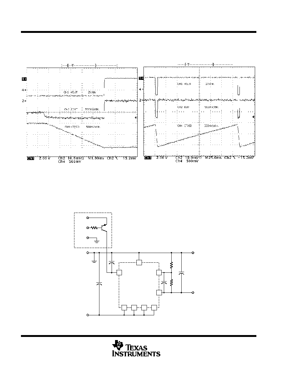
Figure 6 and Figure 7 are oscilloscope photos of the UCC384ÙADJ operating during an overcurrent condition.
Figure 6 shows operation of the circuit as the output current initially rises above the overcurrent threshold. This
is shown on a 1ms/div. scale. Figure 7 shows operation of the same circuit on a 25 ms/div. scale showing one
complete cycle of operation during an overcurrent condition.
UCC284Ù5, UCC284Ù12, UCC284ÙADJ, UCC384Ù5, UCC384Ù12, UCC384ÙADJ
LOW-DROPOUT 0.5-A NEGATIVE LINEAR REGULATOR
SLUS234D Ù JANUARY 2000 Ù REVISED FEBRUARY 2002
10
POST OFFICE BOX 655303
ñ
DALLAS, TEXAS 75265
APPLICATION INFORMATION
Figure 6
UCC384ÙADJ
OVERCURRENT CONDITION OPERATION
1 ms/div
Figure 7
UCC384ÙADJ
OVERCURRENT CONDITION OPERATION
25 ms/div
shutdown feature of the UCC384
The shutdown feature of the UCC384 allows the device to be placed in a low quiescent current mode. The
UCC384 is shut down by pulling the SD/CT pin more positive than Ù0.7 V with respect to GND. Figure 8 shows
how a shutdown circuit can be configured for the UCC384 using a standard transistor-transistor logic signal to
control it.
UDGÙ99032
5
4
1
3
2
R1
R2
VOUT
VOUTS
GND
6
7
VIN
VIN
VIN
VIN
CIN
VIN
8
CT
SD/CT
COUT
VOUT
+
+
(+)
(+)
(Ù)
C1
UCC384ÙADJ
TTL SHUTDOWN CIRCUIT
1
ç
F
0.015
ç
F
4.7
ç
F
470 k
+5 V
LOGIC
INPUT
+5 V
GND
(Ù)
Figure 8. TTL Controlled Shutdown Circuit for the UCC384
UCC284Ù5, UCC284Ù12, UCC284ÙADJ, UCC384Ù5, UCC384Ù12, UCC384ÙADJ
LOW-DROPOUT 0.5-A NEGATIVE LINEAR REGULATOR
SLUS234D Ù JANUARY 2000 Ù REVISED FEBRUARY 2002
11
POST OFFICE BOX 655303
ñ
DALLAS, TEXAS 75265
APPLICATION INFORMATION
controlling the SD/CT pin
Forcing the SD/CT pin to any fixed voltage affects the operation of the circuit. As mentioned before, pulling the
SD/CT pin more positive than Ù0.7 V puts the circuit in a shutdown mode, limiting the quiescent current to less
than 45
ç
A. Pulling this pin more positive than 6 V with respect to GND damages the device.
Forcing the SD/CT pin to any fixed voltage between Ù0.7 V and Ù1.6 V with respect to GND enables the output.
However, in an overcurrent condition, the output does not pulse at a 2.5% duty cycle, but the output current is
still limited to the peak current limit. This circuit may be used where a fixed current limit is needed, where a 2.5%
duty cycle is undesirable. The UCC384 supplies a maximum current in this configuration as long as the
temperature of the device does not exceed the overtemperature shutdown. This is determined by the peak
current being supplied, the input and output voltages, and the type of heat sink being used. Thermal design
is discussed later on in this data sheet.
Forcing the SD/CT pin to a voltage level between approximately Ù1.6 V and Ù2.6 V with respect to GND is not
recommended as the output may or may not be enabled.
Forcing the SD/CT pin to a voltage level between approximately Ù2.6 V and Ù5 V with respect to GND turns the
output off completely. The output remains off as long as the voltage is applied. Pulling this pin more negative
than Ù5 V with respect to GND damages the device (see Table 1).
Table 1 SD/CT Voltage Levels
SD/CT
STATE
6 V to Ù0.7 V
Output disabled and device in low quiescent shutdown mode.
Ù0.7 V to Ù1.6 V
Output enabled
Ù1.6 V to Ù2.6 V
Output enabled or disabled depending on the previous state.
Ù2.6 V to Ù5 V
Output disabled
Figure 9
VIN TO VOUT DELAY TIME
DURING POWER-UP WITH CT = 0.22
ç
F
UCC284Ù5, UCC284Ù12, UCC284ÙADJ, UCC384Ù5, UCC384Ù12, UCC384ÙADJ
LOW-DROPOUT 0.5-A NEGATIVE LINEAR REGULATOR
SLUS234D Ù JANUARY 2000 Ù REVISED FEBRUARY 2002
12
POST OFFICE BOX 655303
ñ
DALLAS, TEXAS 75265
APPLICATION INFORMATION
VIN to VOUT Delay
During power-up there is a delay between VIN and VOUT. The majority of this delay time is due to the charging
time of the CT capacitor. When VIN moves more negative than the UVLO of the device with respect to GND,
the CT capacitor begins to charge. A 17-
ç
A current sink is used only during power up to charge the CT capacitor.
When the voltage on the SD/CT pin reaches approximately Ù1.6 V with respect to GND, the output turns on and
regulates. The larger the value of the CT capacitor, the greater the delay time between VIN and VOUT. Figure 9
shows the VIN to VOUT start-up delay, approximately 16 ms for a circuit with CT = 0.22
ç
F.
Shorter delay times can be achieved with a smaller CT capacitor. The problem with a smaller CT capacitor is
that with a very large load, the circuit may stay in overcurrent mode and never turn on. A circuit with a large
capacitive load needs a large CT capacitor to operate properly.
One way to shorten the delay from VIN to VOUT during powerup, is with the use of the quick start-up circuit
shown in Figure 10.
UDGÙ99033
5
4
1
3
2
R1
R2
VOUT
VOUTS
GND
6
7
VIN
VIN
VIN
VIN
CIN
VIN
8
CT
SD/CT
COUT
VOUT
+
+
(+)
(+)
C1
UCC384ÙADJ
R3
C2
2N7000
QUICK START CURRENT
R4
0.22
ç
F
0.1
ç
F
18 k
12 k
1
ç
F
4.7
ç
F
Q1
(Ù)
(Ù)
Figure 10. Quick Start-Up Circuit for UCC384
With the quick start-up circuit, the delay time between VIN and VOUT during start-up can be reduced
dramatically. Figure 11 shows that with the quick start-up circuit, the VIN to VOUT delay time has been reduced
to approximately 1 ms.

UCC284Ù5, UCC284Ù12, UCC284ÙADJ, UCC384Ù5, UCC384Ù12, UCC384ÙADJ
LOW-DROPOUT 0.5-A NEGATIVE LINEAR REGULATOR
SLUS234D Ù JANUARY 2000 Ù REVISED FEBRUARY 2002
13
POST OFFICE BOX 655303
ñ
DALLAS, TEXAS 75265
APPLICATION INFORMATION
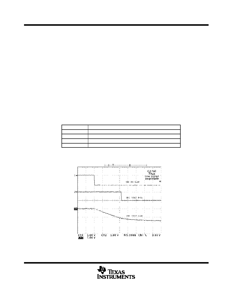
VIN to VOUT Delay
Figure 11
VIN TO VOUT DELAY TIME
WITH QUICK START-UP CIRCUIT
Figure 12
VIN TO VOUT DELAY TIME
WITH CT CAPACITOR REMOVED
operation of the quick start-up circuit
During normal start-up, the UCC384 does not turn on until the voltage on the SD/CT pin reaches approximately
Ù1.6 V with respect to ground. It takes a certain amount of time for the CT capacitor to charge to this point. For
a circuit that has a very large load, the CT capacitor needs to be large in order for the overcurrent timing to work
properly. A large value of capacitance on the SD/CT pin increases the VIN to VOUT delay time.
The quick start-up circuit uses Q1 to quickly pull the SD/CT pin in a negative direction during start-up, thus
decreasing the VIN-to-VOUT delay time. When VIN is applied to the circuit, Q1 turns on and starts to charge
the CT capacitor. The current pulled through R4 determines the rate at which CT is charged. R4 can be
calculated as follows:
R4
+
V
IN
(V)
T
D
seconds
1.6
CT (F)
ohms
(6)
t
D
is the approximate VIN-to-VOUT delay time desired.
Q1 needs to be turned off after a fixed time to prevent the SD/CT pin from going too far negative with respect
to GND. If the SD/CT pin is allowed to go too far negative with respect to GND, the output turns off again or
possibly even damages the SD/CT pin. The maximum amount of time that Q1 should be allowed to be on is
referred to as t
M
and can be calculated as follows:
t
M
+
2.6
1.6
t
D
seconds
(7)
R3 along with C2 set the time that Q1 is allowed to be on. Since t
M
is the maximum amount of time that Q1 should
be allowed to stay on, an added safety margin may be to use 0.9
æ
t
M
instead. This ensures that Q1 is turned
off in the proper amount of time. With a chosen value for C2, R3 can be calculated as follows:

UCC284Ù5, UCC284Ù12, UCC284ÙADJ, UCC384Ù5, UCC384Ù12, UCC384ÙADJ
LOW-DROPOUT 0.5-A NEGATIVE LINEAR REGULATOR
SLUS234D Ù JANUARY 2000 Ù REVISED FEBRUARY 2002
14
POST OFFICE BOX 655303
ñ
DALLAS, TEXAS 75265
APPLICATION INFORMATION
operation of the quick start-up circuit (continued)
R3
+
0.9
t
M
seconds
C2(F)
n
1
*
V
IN
(V)
*
1.6
V
IN
(V)
Ohms
(8)
After the CT capacitor has charged up for a time equal to 0.9
æ
t
M
, Q1 turns off and allows the SD/CT pin to
be pulled back to Ù1.5 V with respect to GND through a 50-k
resistor. At this point , the SD/CT pin can be used
by the UCC384 overcurrent timing control.
minimum V
IN
to V
OUT
delay time
Although it may desirable to have as short a delay time as possible, a small portion of this delay time is fixed
by the UCC384 and cannot be shortened. This is shown in Figure 12, where the CT capacitor has been removed
from the circuit completely, giving a fixed VIN to VOUT delay of approximately 150
ç
s for a circuit with VIN = Ù6 V
and VOUT = Ù5 V.
thermal design
The Packaging Information section of the Power Supply Control Products Data Book (TI Literature
No. SLUD003) contains reference material for the thermal ratings of various packages. The section also
includes an excellent article entitled Thermal Characteristics of Surface Mount Packages, which is the basis
for the following discussion.
Thermal design for the UCC384 includes two modes of operation, normal and pulsed. In normal mode, the linear
regulator and heat sink must dissipate power equal to the maximum forward voltage drop multiplied by the
maximum load current. Assuming a constant current load, the expected heat rise at the regulator's junction can
be calculated as follows:
t
RISE
+
P
DISS
(
q
jc
) q
ca)
(9)
Theta (
) is the thermal resistance and P
DISS
is the power dissipated. The junction-to-case thermal resistance
(
jc) of the SOICÙ8 DP package is 22
¯
C/W. In order to prevent the regulator from going into thermal shutdown,
the case-to-ambient thermal resistance (
ca) must keep the junction temperature below 150
¯
C. If the UCC384
is mounted on a 5 square inch pad of 1-ounce copper, for example, the thermal resistance (
ja) becomes
40Ù70
¯
C/W. If a lower thermal resistance is required for the application, the device heat sinking needs to be
improved.
When the UCC384 is in a pulsed mode, due to an overcurrent condition, the maximum average power
dissipation is calculated as follows:
Pavg
+
V
IN
(V)
*
V
OUT
(V)
I
PEAK
(A)
t
ON
(seconds)
40
t
ON
(seconds)
Watts
(10)
As seen in equation (10), the average power during a fault is reduced dramatically by the duty cycle, allowing
the heat sink to be sized for normal operation. Although the peak power in the regulator during the t
ON
period
can be significant, the thermal mass of the package normally keeps the junction temperature from rising unless
the t
ON
period is increased to several milliseconds.
PACKAGING INFORMATION
Orderable Device
Status
(1)
Package
Type
Package
Drawing
Pins Package
Qty
Eco Plan
(2)
Lead/Ball Finish
MSL Peak Temp
(3)
UCC284DP-12
ACTIVE
SOIC
D
8
75
Green (RoHS &
no Sb/Br)
CU NIPDAU
Level-2-260C-1 YEAR
UCC284DP-5
ACTIVE
SOIC
D
8
75
Green (RoHS &
no Sb/Br)
CU NIPDAU
Level-2-260C-1 YEAR
UCC284DP-5G4
ACTIVE
SOIC
D
8
75
Green (RoHS &
no Sb/Br)
CU NIPDAU
Level-2-260C-1 YEAR
UCC284DP-ADJ
ACTIVE
SOIC
D
8
75
Green (RoHS &
no Sb/Br)
CU NIPDAU
Level-2-260C-1 YEAR
UCC284DP-ADJG4
ACTIVE
SOIC
D
8
75
Green (RoHS &
no Sb/Br)
CU NIPDAU
Level-2-260C-1 YEAR
UCC284DPTR-5
ACTIVE
SOIC
D
8
2500 Green (RoHS &
no Sb/Br)
CU NIPDAU
Level-2-260C-1 YEAR
UCC284DPTR-5G4
ACTIVE
SOIC
D
8
2500 Green (RoHS &
no Sb/Br)
CU NIPDAU
Level-2-260C-1 YEAR
UCC284DPTR-ADJ
ACTIVE
SOIC
D
8
2500 Green (RoHS &
no Sb/Br)
CU NIPDAU
Level-2-260C-1 YEAR
UCC284DPTR-ADJG4
ACTIVE
SOIC
D
8
2500 Green (RoHS &
no Sb/Br)
CU NIPDAU
Level-2-260C-1 YEAR
UCC384DP-12
ACTIVE
SOIC
D
8
75
Green (RoHS &
no Sb/Br)
CU NIPDAU
Level-2-260C-1 YEAR
UCC384DP-5
ACTIVE
SOIC
D
8
75
Green (RoHS &
no Sb/Br)
CU NIPDAU
Level-2-260C-1 YEAR
UCC384DP-5G4
ACTIVE
SOIC
D
8
75
Green (RoHS &
no Sb/Br)
CU NIPDAU
Level-2-260C-1 YEAR
UCC384DP-ADJ
ACTIVE
SOIC
D
8
75
Green (RoHS &
no Sb/Br)
CU NIPDAU
Level-2-260C-1 YEAR
UCC384DP-ADJG4
ACTIVE
SOIC
D
8
75
Green (RoHS &
no Sb/Br)
CU NIPDAU
Level-2-260C-1 YEAR
UCC384DPTR-12
ACTIVE
SOIC
D
8
2500 Green (RoHS &
no Sb/Br)
CU NIPDAU
Level-2-260C-1 YEAR
UCC384DPTR-5
ACTIVE
SOIC
D
8
2500 Green (RoHS &
no Sb/Br)
CU NIPDAU
Level-2-260C-1 YEAR
UCC384DPTR-ADJ
ACTIVE
SOIC
D
8
2500 Green (RoHS &
no Sb/Br)
CU NIPDAU
Level-2-260C-1 YEAR
UCC384DPTR-ADJG4
ACTIVE
SOIC
D
8
2500 Green (RoHS &
no Sb/Br)
CU NIPDAU
Level-2-260C-1 YEAR
(1)
The marketing status values are defined as follows:
ACTIVE: Product device recommended for new designs.
LIFEBUY: TI has announced that the device will be discontinued, and a lifetime-buy period is in effect.
NRND: Not recommended for new designs. Device is in production to support existing customers, but TI does not recommend using this part in
a new design.
PREVIEW: Device has been announced but is not in production. Samples may or may not be available.
OBSOLETE: TI has discontinued the production of the device.
(2)
Eco
Plan
-
The
planned
eco-friendly
classification:
Pb-Free
(RoHS)
or
Green
(RoHS
&
no
Sb/Br)
-
please
check
http://www.ti.com/productcontent
for the latest availability information and additional product content details.
TBD: The Pb-Free/Green conversion plan has not been defined.
Pb-Free (RoHS): TI's terms "Lead-Free" or "Pb-Free" mean semiconductor products that are compatible with the current RoHS requirements
for all 6 substances, including the requirement that lead not exceed 0.1% by weight in homogeneous materials. Where designed to be soldered
at high temperatures, TI Pb-Free products are suitable for use in specified lead-free processes.
Green (RoHS & no Sb/Br): TI defines "Green" to mean Pb-Free (RoHS compatible), and free of Bromine (Br) and Antimony (Sb) based flame
PACKAGE OPTION ADDENDUM
www.ti.com
27-Sep-2005
Addendum-Page 1
retardants (Br or Sb do not exceed 0.1% by weight in homogeneous material)
(3)
MSL, Peak Temp. -- The Moisture Sensitivity Level rating according to the JEDEC industry standard classifications, and peak solder
temperature.
Important Information and Disclaimer:The information provided on this page represents TI's knowledge and belief as of the date that it is
provided. TI bases its knowledge and belief on information provided by third parties, and makes no representation or warranty as to the
accuracy of such information. Efforts are underway to better integrate information from third parties. TI has taken and continues to take
reasonable steps to provide representative and accurate information but may not have conducted destructive testing or chemical analysis on
incoming materials and chemicals. TI and TI suppliers consider certain information to be proprietary, and thus CAS numbers and other limited
information may not be available for release.
In no event shall TI's liability arising out of such information exceed the total purchase price of the TI part(s) at issue in this document sold by TI
to Customer on an annual basis.
PACKAGE OPTION ADDENDUM
www.ti.com
27-Sep-2005
Addendum-Page 2

IMPORTANT NOTICE
Texas Instruments Incorporated and its subsidiaries (TI) reserve the right to make corrections, modifications,
enhancements, improvements, and other changes to its products and services at any time and to discontinue
any product or service without notice. Customers should obtain the latest relevant information before placing
orders and should verify that such information is current and complete. All products are sold subject to TI's terms
and conditions of sale supplied at the time of order acknowledgment.
TI warrants performance of its hardware products to the specifications applicable at the time of sale in
accordance with TI's standard warranty. Testing and other quality control techniques are used to the extent TI
deems necessary to support this warranty. Except where mandated by government requirements, testing of all
parameters of each product is not necessarily performed.
TI assumes no liability for applications assistance or customer product design. Customers are responsible for
their products and applications using TI components. To minimize the risks associated with customer products
and applications, customers should provide adequate design and operating safeguards.
TI does not warrant or represent that any license, either express or implied, is granted under any TI patent right,
copyright, mask work right, or other TI intellectual property right relating to any combination, machine, or process
in which TI products or services are used. Information published by TI regarding third-party products or services
does not constitute a license from TI to use such products or services or a warranty or endorsement thereof.
Use of such information may require a license from a third party under the patents or other intellectual property
of the third party, or a license from TI under the patents or other intellectual property of TI.
Reproduction of information in TI data books or data sheets is permissible only if reproduction is without
alteration and is accompanied by all associated warranties, conditions, limitations, and notices. Reproduction
of this information with alteration is an unfair and deceptive business practice. TI is not responsible or liable for
such altered documentation.
Resale of TI products or services with statements different from or beyond the parameters stated by TI for that
product or service voids all express and any implied warranties for the associated TI product or service and
is an unfair and deceptive business practice. TI is not responsible or liable for any such statements.
Following are URLs where you can obtain information on other Texas Instruments products and application
solutions:
Products
Applications
Amplifiers
amplifier.ti.com
Audio
www.ti.com/audio
Data Converters
dataconverter.ti.com
Automotive
www.ti.com/automotive
DSP
dsp.ti.com
Broadband
www.ti.com/broadband
Interface
interface.ti.com
Digital Control
www.ti.com/digitalcontrol
Logic
logic.ti.com
Military
www.ti.com/military
Power Mgmt
power.ti.com
Optical Networking
www.ti.com/opticalnetwork
Microcontrollers
microcontroller.ti.com
Security
www.ti.com/security
Telephony
www.ti.com/telephony
Video & Imaging
www.ti.com/video
Wireless
www.ti.com/wireless
Mailing Address:
Texas Instruments
Post Office Box 655303 Dallas, Texas 75265
Copyright
2005, Texas Instruments Incorporated