 | –≠–ª–µ–∫—Ç—Ä–æ–Ω–Ω—ã–π –∫–æ–º–ø–æ–Ω–µ–Ω—Ç: UCC28501N | –°–∫–∞—á–∞—Ç—å:  PDF PDF  ZIP ZIP |

UCC28500, UCC28501, UCC28502, UCC28503
UCC38500, UCC38501, UCC38502, UCC38503
SLUS419C ≠ AUGUST 1999 ≠ REVISED NOVEMBER 2001
BiCMOS PFC/PWM
COMBINATION CONTROLLER
1
www.ti.com
FEATURES
D
Combines PFC and Downstream Converter
Controls
D
Controls Boost Preregulator to Near-Unity
Power Factor
D
Accurate Power Limiting
D
Improved Feedforward Line Regulation
D
Peak Current-Mode Control in Second Stage
D
Programmable Oscillator
D
Leading-Edge/Trailing-Edge Modulation for
Reduced Output Ripple
D
Low Start-up Supply Current
D
Synchronized Second Stage Start-Up, with
Programmable Soft-start
D
Programmable Second Stage Shutdown
DESCRIPTION
The UCC2850x family provides all of the control
functions necessary for an active power-factor-
corrected preregulator and a second-stage dc-to- dc
converter. The controller achieves near-unity power
factor by shaping the ac input line current waveform to
correspond to the ac input-line voltage using average
current-mode control. The dc-to-dc converter uses
peak current-mode control to perform the step-down
power conversion.
The PFC stage is leading-edge modulated while the
second stage is trailing-edge synchronized to allow for
minimum overlap between the boost and PWM
switches. This reduces ripple current in the bulk-output
capacitor.In order to operate with over three-to-one
range of input-line voltages, a line feedforward (V
FF
) is
used to keep input power constant with varying input
voltage. Generation of V
FF
is accomplished using I
AC
in
conjunction with an external single-pole filter. This not
only reduces external parts count, but also avoids the
use of high-voltage components, offering a lower-cost
solution. The multiplier then divides the line current by
the square of V
FF
.
The UCC2850x PFC section incorporates a low
offset-voltage amplifier with 7.5-V reference, a
highly-linear multiplier capable of a wide current range,
a high-bandwidth, low offset-current amplifier, with a
novel noise-attenuation configuration, PWM
comparator and latch, and a high-current output driver.
Additional PFC features include over-voltage
protection, zero-power detection to turn off the output
when VAOUT is below 0.33 V and peak current and
power limiting.
The dc-to-dc section relies on an error signal generated
on the secondary-side and processes it by performing
peak current mode control. The dc-to-dc section also
features current limiting, a controlled soft-start, preset
operating range with selectable options, and 50%
maximum duty cycle.
The UCC28500 and UCC28502 have a wide
PFC-UVLO threshold (16.5 V/10 V) for bootstrap bias
supply operation. The UCC28501 and UCC28503 are
designed with a narrow UVLO range (10.5 V/10 V) more
suitable for fixed bias operation. The UCC28500 and
UCC28501 have a narrow UVLO threshold for PWM
stage (to allow operation down to 75% of nominal bulk
voltage), while the UCC28502 and UCC38503 are
configured for a much wider operation range for the
PWM stage (down to 50% of bulk nominal voltage).
Available in 20-pin N and DW packages.
PRODUCTION DATA information is current as of publication date.
Products conform to specifications per the terms of Texas Instruments
standard warranty. Production processing does not necessarily include
testing of all parameters.
Copyright
2001, Texas Instruments Incorporated
UCC28500, UCC28501, UCC28502, UCC28503
UCC38500, UCC38501, UCC38502, UCC38503
SLUS419C ≠ AUGUST 1999 ≠ REVISED NOVEMBER 2001
2
www.ti.com
absolute maximum ratings over operating free-air temperature (unless otherwise noted)
Supply Voltage VCC
18 V
. . . . . . . . . . . . . . . . . . . . . . . . . . . . . . . . . . . . . . . . . . . . . . . . . . . . . . . . . . . . . . . . . . . . . . . .
Gate Drive Current
Continuous
0.2 A
. . . . . . . . . . . . . . . . . . . . . . . . . . . . . . . . . . . . . . . . . . . . . . . . . . . . . . . . . . . . . . . . . . . . . . . . . . . . .
Pulsed
1.2 A
. . . . . . . . . . . . . . . . . . . . . . . . . . . . . . . . . . . . . . . . . . . . . . . . . . . . . . . . . . . . . . . . . . . . . . . . . . . . . . . .
Input Voltage
ISENSE1, ISENSE2, MOUT, VSENSE, OVP/ENBL
10 V
. . . . . . . . . . . . . . . . . . . . . . . . . . . . . . . . . . . . . . . . . .
CAI, MOUT, CT
8 V
. . . . . . . . . . . . . . . . . . . . . . . . . . . . . . . . . . . . . . . . . . . . . . . . . . . . . . . . . . . . . . . . . . . . . . . . . .
PKLMT, VERR
5 V
. . . . . . . . . . . . . . . . . . . . . . . . . . . . . . . . . . . . . . . . . . . . . . . . . . . . . . . . . . . . . . . . . . . . . . . . . . .
Input Current
RSET, RT, IAC, PKLMT, ENA
10 mA
. . . . . . . . . . . . . . . . . . . . . . . . . . . . . . . . . . . . . . . . . . . . . . . . . . . . . . . . . . . .
VCC (no switching)
20 mA
. . . . . . . . . . . . . . . . . . . . . . . . . . . . . . . . . . . . . . . . . . . . . . . . . . . . . . . . . . . . . . . . . . . . .
Maximum Negative Voltage GT1, GT2, PKLMT, MOUT
≠0.5 V
. . . . . . . . . . . . . . . . . . . . . . . . . . . . . . . . . . . . . . . . .
Power Dissipation
1 W
. . . . . . . . . . . . . . . . . . . . . . . . . . . . . . . . . . . . . . . . . . . . . . . . . . . . . . . . . . . . . . . . . . . . . . . . . . .
Storage temperature T
stg
≠65
∞
C to 150
∞
C
. . . . . . . . . . . . . . . . . . . . . . . . . . . . . . . . . . . . . . . . . . . . . . . . . . . . . . . . . .
Junction temperature T
J
≠55
∞
C to 125
∞
C
. . . . . . . . . . . . . . . . . . . . . . . . . . . . . . . . . . . . . . . . . . . . . . . . . . . . . . . . . .
Lead temperature (soldering, 10 sec)
300
∞
C
. . . . . . . . . . . . . . . . . . . . . . . . . . . . . . . . . . . . . . . . . . . . . . . . . . . . . . . .
Stresses beyond those listed under "absolute maximum ratings" may cause permanent damage to the device. These are stress ratings only, and
functional operation of the device at these or any other conditions beyond those indicated under recommended operating conditions is not implied.
Exposure to absolute-maximum-rated conditions for extended periods may affect device reliability.
Currents are positive into, negative out of the specified terminal. Consult Packaging Section of Databook for thermal limitations and
considerations of packages. All voltages are referenced to GND.
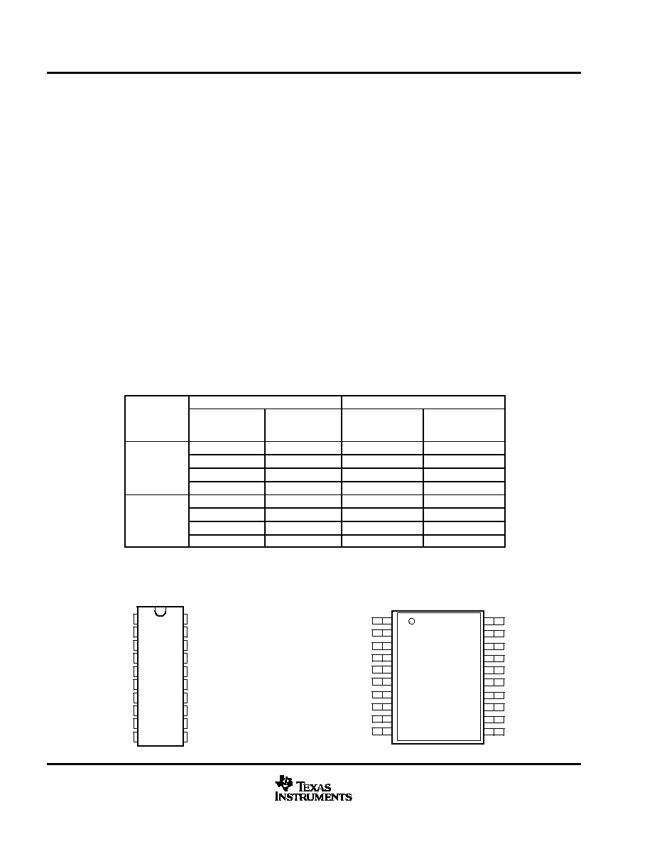
AVAILABLE OPTIONS
PFC THRESHOLD
PACKAGED DEVICES
TJ
PFC UVLO
TURN≠ON
THRESHOLD (V)
UVLO2
HYSTERESIS
(V)
PLASTIC DIP
(N)
SMALL OUTLINE
(DW)
16
1.2
UCC28500N
UCC28500DW
40
∞
C to 85
∞
C
10.5
1.2
UCC28501N
UCC28501DW
≠40
∞
C to 85
∞
C
16
3.0
UCC28502N
UCC28502DW
10.5
3.0
UCC28503N
UCC28503DW
16
1.2
UCC38500N
UCC38500DW
0
∞
C to 70
∞
C
10.5
1.2
UCC38501N
UCC38501DW
0
∞
C to 70
∞
C
16
3.0
UCC38502N
UCC38502DW
10.5
3.0
UCC38503N
UCC38503DW
The DW package is available taped and reeled. Add TR suffix to device type (e.g. UCC38500DWTR)
to order quantities of 2000 devices per reel.
1
2
3
4
5
6
7
8
9
10
20
19
18
17
16
15
14
13
12
11
VAOUT
RT
VSENSE
OVP/ENBL
CT
GND
VERR
ISENSE2
VCC
GT2
VREF
VFF
IAC
MOUT
ISENSE1
CAOUT
PKLMT
SS2
GT1
PWRGND
N PACKAGE
(TOP VIEW)
1
2
3
4
5
6
7
8
9
10
20
19
18
17
16
15
14
13
12
11
VAOUT
RT
VSENSE
OVP/ENBL
CT
GND
VERR
ISENSE2
VCC
GT2
VREF
VFF
IAC
MOUT
ISENSE1
CAOUT
PKLMT
SS2
GT1
PWRGND
DW PACKAGE
(TOP VIEW)
UCC28500, UCC28501, UCC28502, UCC28503
UCC38500, UCC38501, UCC38502, UCC38503
SLUS419C ≠ AUGUST 1999 ≠ REVISED NOVEMBER 2001
3
www.ti.com
electrical characteristics T
A
= 0
∞
C to 70
∞
C for the UCC3850X, ≠40
∞
C to 85
∞
C for the UCC2850X,
T
A
= T
J
, VCC = 12 V, RT = 22 k
, CT = 330 pF (unless otherwise noted)
supply current
PARAMETER
TEST CONDITIONS
MIN
TYP
MAX
UNITS
Supply current, off
VCC turn-on threshold ≠300 mV
150
300
µ
A
Supply current, on
VCC = 12 V (no load on GT1 or GT2)
4
6
mA
undervoltage lockout
PARAMETER
TEST CONDITIONS
MIN
TYP
MAX
UNITS
VCC turn-on threshold (UCCx8500/502)
15.4
16
16.6
V
UVLO hysteresis (UCCx8500/502)
5.8
6.3
V
Shunt voltage (UCCx8500/502)
IVCC = 10 mA
15.4
16.2
17.0
V
VCC turn-on threshold (UCCx8501/503)
9.7
10.2
10.8
V
VCC turn-off threshold
9.4
9.7
V
UVLO hysteresis (UCCx8501/503)
0.3
0.5
V
voltage amplifier
PARAMETER
TEST CONDITIONS
MIN
TYP
MAX
UNITS
Inp t oltage
0
∞
C
TA
70
∞
C
7.387
7.500
7.613
V
Input voltage
≠40
∞
C
TA
85
∞
C
7.35
7.50
7.65
V
VSENSE bias current
50
200
nA
Open loop gain
VAOUT = 2 V to 5 V
50
90
dB
High-level output voltage
ILOAD = ≠150
µ
A
5.3
5.5
5.6
V
Low-level output voltage
ILOAD = 150
µ
A
0.00
0.05
0.15
V
overvoltage protection and enable
PARAMETER
TEST CONDITIONS
MIN
TYP
MAX
UNITS
Over voltage reference
VREF
+ 0.480
VREF
+ 0.500
VREF
+ 0.520
V
Hysteresis
300
500
600
mV
Enable threshold
1.7
1.9
2.1
V
Enable hysteresis
0.1
0.2
0.3
V
current amplifier
PARAMETER
TEST CONDITIONS
MIN
TYP
MAX
UNITS
Input offset voltage
VCM = 0 V,
VCAOUT = 3 V
≠6
0
6
mV
Input bias current
VCM = 0 V,
VCAOUT = 3 V
≠50
≠100
nA
Input offset current
VCM = 0 V,
VCAOUT = 3 V
25
100
nA
Open loop gain
VCM = 0 V,
VCAOUT = 2 V to 5 V
90
dB
Common≠mode rejection ratio
VCM = 0 V to 1.5 V, VCAOUT = 3 V
90
dB
High-level output voltage
ILOAD = ≠120
µ
A
5.6
7.0
7.5
V
Low-level output voltage
ILOAD = 1 mA
0.1
0.2
0.5
V
Gain bandwidth product
See Note 1
2.5
MHz
NOTES:
1. Ensured by design. Not production tested.
2. See Figure 6 for reference variation.
3. See Figure 5 for reference variation for VCC < 10.8 V.
UCC28500, UCC28501, UCC28502, UCC28503
UCC38500, UCC38501, UCC38502, UCC38503
SLUS419C ≠ AUGUST 1999 ≠ REVISED NOVEMBER 2001
4
www.ti.com
electrical characteristics T
A
= 0
∞
C to 70
∞
C for the UCC3850X, ≠40
∞
C to 85
∞
C for the UCC2850X,
T
A
= T
J
, VCC = 12 V, RT = 22 k
, CT = 330 pF (unless otherwise noted)
voltage reference
PARAMETER
TEST CONDITIONS
MIN
TYP
MAX
UNITS
Inp t oltage
TA = 0
∞
C to 70
∞
C
7.387
7.500
7.613
V
Input voltage
TA = ≠40
∞
C to 85
∞
C
7.35
7.50
7.65
V
Load regulation
IREF = ≠1 mA to ≠2 mA,
See Note 2
0
10
mV
Line regulation
VCC = 10.8 V to 15 V,
See Note 3
0
10
mV
Short circuit current
VREF = 0V
≠20
≠25
≠50
mA
oscillator
PARAMETER
TEST CONDITIONS
MIN
TYP
MAX
UNITS
Frequency, initial accuracy
TA = 25
∞
C
85
100
115
kHz
Frequency, voltage stability
VCC = 10.8 V to 15 V
≠1%
1%
Frequency, total variation
Line, Temp
80
120
kHz
Ramp peak voltage
4.5
5
5.5
V
Ramp amplitude voltage (peak to peak)
3.5
4
4.5
V
peak current limit
PARAMETER
TEST CONDITIONS
MIN
TYP
MAX
UNITS
PKLMT reference voltage
≠15
0
15
mV
PKLMT propagation delay
150
300
500
ns
multiplier
PARAMETER
TEST CONDITIONS
MIN
TYP
MAX
UNITS
IMOUT, high-line low-power output current
IAC = 500
µ
A, VFF = 4.7 V,
VAOUT = 1.25 V,
0
∞
C
TA
85
∞
C
0
≠6
≠20
IMOUT, high-line low-power output current
IAC = 500
µ
A, VFF = 4.7 V,
VAOUT = 1.25 V,
≠40
∞
C
TA
85
∞
C
0
≠6
≠23
IMOUT, high-line high-power output current
IAC = 500
µ
A, VFF = 4.7 V,
VAOUT = 5 V
≠70
≠90
≠105
µ
A
IMOUT, low-line low-power output current
IAC = 150
µ
A, VFF = 1.4 V,
VAOUT = 1.25 V
≠10
≠19
≠50
IMOUT, low-line high-power output current
IAC = 150
µ
A, VFF = 1.4 V,
VAOUT = 5 V
≠268
≠300
≠345
IMOUT, IAC-limited output current
IAC = 150
µ
A, VFF = 1.3 V,
VAOUT = 5 V
≠250
≠300
≠400
Gain constant (K)
IAC = 300
µ
A, VFF = 2.8 V,
VAOUT = 2.5 V
0.5
1
1.5
1/V
IAC = 150
µ
A, VFF = 1.4 V,
VAOUT = 0.25 V
0
≠2
1/V
IAC = 500
µ
A, VFF = 4.7 V,
VAOUT = 0.25 V
0
≠2
µ
A
IMOUT, zero current
IAC = 500
µ
A, VFF = 4.7 V,
VAOUT = 0.5 V,
0
∞
C
TA
85
∞
C
0
≠3
µ
A
IAC = 500
µ
A, VFF = 4.7 V,
VAOUT = 0.5 V,
≠40
∞
C
TA
85
∞
C
0
≠3.5
µ
A
Power limit (IMOUT
◊
VFF)
IAC = 150
µ
A, VFF = 1.4 V,
VAOUT = 5 V
≠375
≠420
≠485
µ
W
zero power
PARAMETER
TEST CONDITIONS
MIN
TYP
MAX
UNITS
Zero power comparator threshold
Measured on VAOUT
0.175
0.330
0.500
V
NOTES:
1. Ensured by design. Not production tested.
2. See Figure 6 for reference variation.
3. See Figure 5 for reference variation for VCC < 10.8 V .

UCC28500, UCC28501, UCC28502, UCC28503
UCC38500, UCC38501, UCC38502, UCC38503
SLUS419C ≠ AUGUST 1999 ≠ REVISED NOVEMBER 2001
5
www.ti.com
electrical characteristics T
A
= 0
∞
C to 70
∞
C for the UCC3850X, ≠40
∞
C to 85
∞
C for the UCC2850X,
T
A
= T
J
, VCC = 12 V, RT = 22 k
, CT = 330 pF (unless otherwise noted)
PFC gate driver
PARAMETER
TEST CONDITIONS
MIN
TYP
MAX
UNITS
GT1 pull up resistance
IOUT from ≠100 mA to ≠200 mA
5
12
GT1 pull down resistance
IOUT = 100 mA
2
10
GT1 output rise time
CLOAD = 1 nF,
RLOAD = 10
VGT1 from 0.7 V to 9.0 V
25
50
ns
GT1 output fall time
CLOAD = 1 nF,
RLOAD = 10
VGT1 from 9.0 V to 0.7 V
10
50
ns
Maximum duty cycle
93%
95%
100%
Minimum controlled duty cycle
f = 100 kHZ
2%
second stage undervoltage lockout (UVLO2)
PARAMETER
TEST CONDITIONS
MIN
TYP
MAX
UNITS
PWM turn-on reference (UCCx8500/501)
6.30
6.75
7.30
V
Hysteresis (UCCx8500/501)
0.96
1.20
1.44
V
PWM turn≠on reference (UCCx8502/503)
6.30
6.75
7.30
V
Hysteresis (UCCx8502/503)
2.4
3
3.6
V
second stage soft-start
PARAMETER
TEST CONDITIONS
MIN
TYP
MAX
UNITS
SS2 charge current
≠7.3
≠10
≠12.5
µ
A
Input voltage (VERR)
IVERR = 2 mA,UVLO = Low
300
mV
SS2 discharge current
ENBL = High, UVLO = Low, SS2 = 2.5 V
3
10
mA
second stage duty cycle clamp
PARAMETER
TEST CONDITIONS
MIN
TYP
MAX
UNITS
Maximum duty cycle
44%
50%
second stage pulse-by-pulse current sense
PARAMETER
TEST CONDITIONS
MIN
TYP
MAX
UNITS
Current sense comparator threshold
VERR = 2.5 V measured on ISENSE2
0.94
1.05
1.15
V
second stage overcurrent limit
PARAMETER
TEST CONDITIONS
MIN
TYP
MAX
UNITS
Peak current comparator threshold
1.15
1.30
1.45
V
Input bias current
50
nA
second stage gate driver
PARAMETER
TEST CONDITIONS
MIN
TYP
MAX
UNITS
GT2 pull up resistance
IOUT from ≠100 mA to ≠200 mA
5
12
GT2 pull down resistance
IOUT = 100 mA
3
10
GT2 output rise time
CLOAD = 1 nF,RLOAD = 10
VGT2 from 0.7 V to 9.0 V
25
50
ns
GT2 output fall time
CLOAD = 1 nF,RLOAD = 10
VGT2 from 9.0 V to 0.7 V
25
50
ns
NOTES:
1. Ensured by design. Not production tested.
2. See Figure 6 for reference variation.
3. See Figure 5 for reference variation for VCC < 10.8 V .

UCC28500, UCC28501, UCC28502, UCC28503
UCC38500, UCC38501, UCC38502, UCC38503
SLUS419C ≠ AUGUST 1999 ≠ REVISED NOVEMBER 2001
6
www.ti.com
pin assignments
CAOUT: (current amplifier output) This is the output of a wide bandwidth operational amplifier that senses line
current and commands the PFC pulse width modulator (PWM) to force the correct duty cycle. This output can
swing close to GND, allowing the PWM to force zero duty cycle when necessary.
CT: (oscillator timing capacitor) A capacitor from CT to GND sets the oscillator frequency according to:
f
+
0.725
R
T
C
T
GND: (ground) All voltages measured with respect to ground. VCC and VREF should be bypassed directly to
GND with a 0.1-
µ
F or larger ceramic capacitor. The timing capacitor discharge current also returns to this pin,
so the lead from the oscillator timing capacitor to GND should be as short and direct as possible.
GT1: (gate drive) The output drive for the PFC stage is a totem pole MOSFET gate driver on GT1. Use a series
gate resistor of at least 10.5
to prevent interaction between the gate impedance and the GT1 output driver
that might cause the GT1 to overshoot excessively. Some overshoot of the GT1 output is always expected when
driving a capacitive load. Refer to Figure 4 for gate drive resistor selections.
GT2: (gate drive) Same as output GT1 for the second stage output drive. Limited to 50% maximum duty cycle.
IAC: (input ac current) This input to the analog multiplier is a current. The multiplier is tailored for very low
distortion from this current input (I
AC
) to MOUT, so this is the only multiplier input which should be used for
sensing instantaneous line voltage. Recommended maximum I
AC
is 500
µ
A.
ISENSE1: (current sense) This is the non-inverting input to the current amplifier. This input and the inverting
input MOUT remain functional down to and below GND.
ISENSE2: (current sense) A resistor from the source of the lower FET to ground generates the input signal for
the peak limit control of the second stage. The oscillator ramp can also be summed into this pin, for slope
compensation.
MOUT: (multiplier output and current sense amplifier inverting input) The output of the analog multiplier and the
inverting input of the current amplifier are connected together at MOUT. As the multiplier output is a current, this
is a high impedance input so the amplifier can be configured as a differential amplifier to reject ground noise.
Multiplier output current is given by:
I
MOUT
+
V
VAOUT
*
1.0
I
IAC
K
V
VFF
2
Connect current loop compensation components between MOUT and CAOUT.
OVP/ENBL: (over-voltage/enable) A window comparator input which disables the PFC output driver if the boost
output is 6.67% above nominal or disables both the PFC and second stage output drivers and reset SS2 if pulled
below 1.9 V. This input is also used to determine the active range of the second stage PWM.
PKLMT: (PFC peak current limit) The threshold for peak limit is 0 V. Use a resistor divider from the negative side
of the current sense resistor to VREF to level-shift this signal to a voltage corresponding to the desired
overcurrent threshold across the current sense resistor.
PWRGND: Ground for totem pole output drivers.
RT: (oscillator charging current) A resistor from RT to GND is used to program oscillator charging current. A
resistor between 10 k
and 100 k
is recommended. Nominal voltage on this pin is 3 V.

UCC28500, UCC28501, UCC28502, UCC28503
UCC38500, UCC38501, UCC38502, UCC38503
SLUS419C ≠ AUGUST 1999 ≠ REVISED NOVEMBER 2001
7
www.ti.com
pin assignments (continued)
SS2: (soft-start for PWM) SS2 is at ground for either enable low or OVP/ENBL below the UVLO2 threshold
conditions. When enabled, SS2 charges an external capacitor with a current source. This voltage is used as
the voltage error signal during start-up, enabling the PWM duty cycle to increase slowly. In the event of a disable
command or a UVLO2 dropout, SS2 quickly discharges to disable the PWM.
VAOUT: (voltage amplifier output) This is the output of the operational amplifier that regulates output voltage.
The voltage amplifier output is internally limited to approximately 5.5 V to prevent overshoot.
VCC: (positive supply voltage) Connect to a stable source of at least 20 mA between 12 V and 17 V for normal
operation. Bypass VCC directly to GND to absorb supply current spikes required to charge external MOSFET
gate capacitances. To prevent inadequate gate drive signals, the output devices are inhibited unless VCC
exceeds the upper under-voltage lockout threshold and remains above the lower threshold.
VERR: (voltage amp error signal for the second stage) The error signal is generated by an external amplifier
which drives this pin. This pin has an internal 4.5-V voltage clamp that limits GT2 to less than 50% duty cycle
to ensure transformer reset in the typical application.
VFF: (RMS feed forward signal) VFF signal is generated at this pin by mirroring one-half of I
AC
into a single pole
external filter. At low line, the VFF voltage should be 1.4 V.
VSENSE: (voltage amplifier inverting input) This is normally connected to a compensation network and to the
boost converter output through a divider network.
VREF: (voltage reference output) VREF is the output of an accurate 7.5-V voltage reference. This output is
capable of delivering 10 mA to peripheral circuitry and is internally short-circuit current limited. VREF is disabled
and remains at 0 V when VCC is below the UVLO threshold. Bypass VREF to GND with a 0.1-
µ
F or larger
ceramic capacitor for best stability.

UCC28500, UCC28501, UCC28502, UCC28503
UCC38500, UCC38501, UCC38502, UCC38503
SLUS419C ≠ AUGUST 1999 ≠ REVISED NOVEMBER 2001
8
www.ti.com
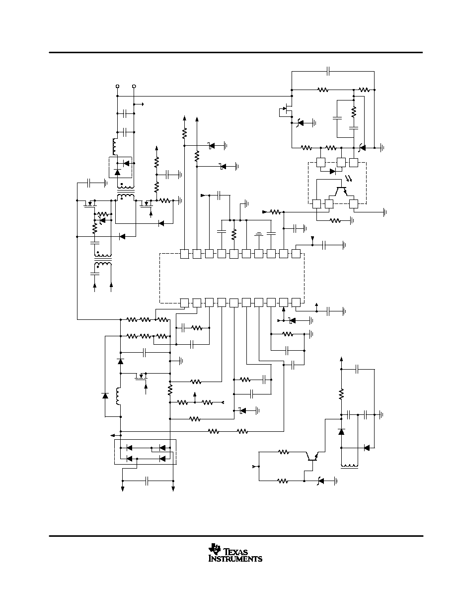
block diagram
UDG≠98189
VREF
20
14
12
11
9
4
17
16
GT1
PWRGND
ISENSE1
VCC
OVP/ENBL
VAOUT
1.9 V
PKLMT
7.5 V
REFERENCE
UVLO
16 V/10 V
10.5 V/10 V
VCC
15
OSCILLATOR
2
RT
5
CT
S
Q
R
PWM
LATCH
CAOUT
SS2
VOLTAGE
ERROR AMP
8.0 V
13
1
3
VSENSE
VFF
19
IAC
18
MOUT
MIRROR
2:1
7.5 V
ENABLE
PFCOVP
˜
X
X
MULT
CLK1
CURRENT
AMP
6.75 V
6
GND
10
GT2
VCC
7
8
CLK2
1.5 V
R
I
LIMIT
CLK2
OSC
CLK1
CLK2
VERR
ISENSE2
I
LIMIT
S
Q
UVLO2
PWM
0.33 V
(V
FF
)
2
ZERO
POWER
SECOND STAGE
SOFT START
+
+
PWM
+
+
+
+
+
+
+
+
4.5 V
PWM 2ND STAGE
SECTION
PFC SECTION
PWM 2ND STAGE
SECTION
PFC SECTION
1.3 V
R
R

UCC28500, UCC28501, UCC28502, UCC28503
UCC38500, UCC38501, UCC38502, UCC38503
SLUS419C ≠ AUGUST 1999 ≠ REVISED NOVEMBER 2001
9
www.ti.com
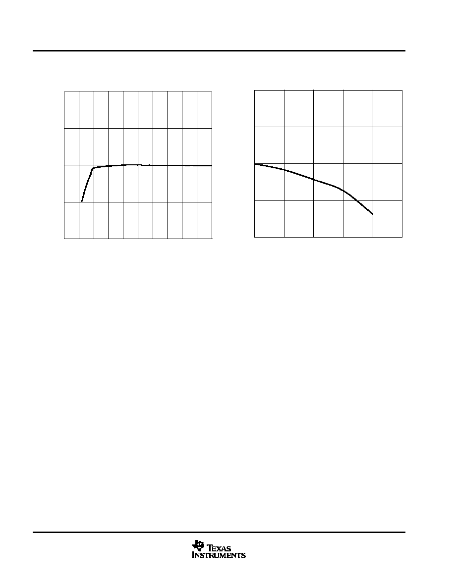
TYPICAL CHARACTERISTICS
Figure 1
MULTIPLIER OUTPUT CURRENT
vs.
VOLTAGE ERROR AMPLIFIER OUTPUT
50
200
250
350
0
100
300
150
IAC = 150
µ
A
IAC = 300
µ
A
IAC = 500
µ
A
I MO
UT
-
Multiplier Output Current
≠
µ
A
VAOUT ≠ Voltage Error Amplifier Output ≠ V
0
1
2
3
4
5
Figure 2
MULTIPLIER GAIN
vs.
VOLTAGE ERROR AMPLIFIER OUTPUT
0.7
1.1
1.3
1.5
0.5
0.9
IAC = 300
µ
A
IAC = 500
µ
A
IAC = 150
µ
A
Multiplier
Gain
≠
K
VAOUT ≠ Voltage Error Amplifier Output ≠ V
1
2
3
4
5
Figure 3
VFF ≠ Feedforward Voltage ≠ V
100
300
400
500
0
200
VAOUT = 3 V
VAOUT = 2 V
VAOUT = 4 V
VAOUT = 5 V
(VFF
◊
I
MO
UT
)
≠
µ
W
MULTIPLIER CONSTANT POWER PERFORMANCE
0
1
2
3
4
5
Figure 4
10
12
14
16
20
10
14
15
17
8
12
18
9
11
13
16
RECOMMENDED MINIMUM GATE RESISTANCE
vs.
SUPPLY VOLTAGE
R
GA
TE
-
Recommended
Minimum Gate Resistance
≠
VCC ≠ Supply Voltage ≠ V
UCC28500, UCC28501, UCC28502, UCC28503
UCC38500, UCC38501, UCC38502, UCC38503
SLUS419C ≠ AUGUST 1999 ≠ REVISED NOVEMBER 2001
10
www.ti.com
Figure 5
14
12
10
7.45
7.50
7.55
7.60
7.40
VCC ≠ Supply Voltage ≠ V
13
11
9
VREF
≠
Reference V
oltage
≠
V
REFERENCE VOLTAGE
vs.
SUPPLY VOLTAGE
Figure 6
REFERENCE VOLTAGE
vs.
REFERENCE CURRENT
0
5
10
15
20
25
7.495
7.500
7.505
7.510
7.490
VREF
≠
Reference V
o
ltage
≠
V
IVREF ≠ Reference Current ≠ mA

UCC28500, UCC28501, UCC28502, UCC28503
UCC38500, UCC38501, UCC38502, UCC38503
SLUS419C ≠ AUGUST 1999 ≠ REVISED NOVEMBER 2001
11
www.ti.com
TYPICAL APPLICATION
The UCC38500 series is designed to incorporate all the control functions required for a power factor correction
circuit and a second stage dc-to-dc converter. The PFC function is implemented as a full-feature,
average-current-mode controller integrated circuit. In addition, the input voltage feedforward function is
implemented in a simplified manner. Current from IAC input is mirrored over to the VFF pin. By simply adding
a resistor and capacitor (to attenuate 120-Hz ripple) a voltage is developed which is proportional to RMS line
voltage, eliminating the need for several components normally connected to the line.
The UCC3850x uses leading-edge modulation for the PFC stage and trailing-edge modulation for the dc-to-dc
stage. This reduces ripple current in the output capacitor by reducing the overlap in conduction time of the PFC
and dc-to-dc switches. Figures 7 and 8 depict the ripple current reduction in the boost switch. In addition to the
reduced ripple current, noise immunity is improved through the current error amplifier implementation. Please
refer to the UCC3817 datasheet (TI Literature No. SLUS395) for a detailed explanation of current error amplifier
implementation.
UDG≠97130≠1
Figure 7. Simplified Representation of a 2≠Stage PFC Power Supply
i
CBST
i
CBST
= i
D1
≠ i
Q2
Figure 8. Timing Waveforms for Synchronization Scheme

UCC28500, UCC28501, UCC28502, UCC28503
UCC38500, UCC38501, UCC38502, UCC38503
SLUS419C ≠ AUGUST 1999 ≠ REVISED NOVEMBER 2001
12
www.ti.com
TYPICAL APPLICATION
The UCC3850x is optimized to control a boost PFC stage operating in continuous conduction mode, followed
by a dc-to-dc converter (typically a forward topology). The dc-to-dc converter is transformer isolated and
therefore its error amplifier is located on the secondary side. For this reason the UCC3850x is configured without
an internal error amplifier for the second power stage. The externally generated error signal is fed into the VERR
pin typically through an opto coupler.
The UCC3850x can be configured for voltage-mode control or current-mode control of the second stage. The
application figure shows a typical current-mode configuration. For voltage-mode control, the ramp generated
by CT can be fed back into the ISENSE2 pin through a voltage divider.
One of the main system challenges in designing systems with a PFC front end is coordinating the turn-on and
turn-off on the dc-to-dc converter. If the dc-to-dc converter is allowed to turn on before the boost converter is
operational, it must operate at a much-reduced voltage and therefore represents a large current draw to the
boost converter. This start-up sequencing is handled internally by the UCC3850x. The UCC3850x monitors the
output voltage of the PFC converter and holds the dc-to-dc converter off until the output is within 10% of its
regulation point. Once the trip point is reached the dc-to-dc section goes through a soft start sequence for a
controlled, low stress start-up. Similarly, if the output voltage drops too low (two voltage options are available)
the dc-to-dc converter shuts down thereby preventing overstress of the converter. For the UCC38500 and
UCC38501, the dc-to-dc converter shuts down when the PFC output falls below 74% of its nominal value, while
for the UCC38502 and UCC38503, the threshold is lowered to 50%.
design example: an off-line, 100-W, power converter
The following design example shows how to implement the UCC38500 in an off-line 100-W power converter.
The system requires the converter to operate from a universal input of 85 V
RMS
to 265 V
RMS
with a 12-V, 100-W,
dc output. This design example is divided into two parts. The first part is the PFC stage design and the second
section is the dc-to-dc power stage design. The design goal of the system is to achieve an efficiency of
approximately 80%. This is accomplished by requiring the boost regulator to be designed for an efficiency of
95% and the dc-to-dc power stage to be designed for 85% efficiency. The efficiency of the boost converter is
designated by variable
1 and the efficiency of the dc-to-dc converter is designated by variable
2. Figure 9
shows the schematic of the typical application upon which this design example is based. The UCC38500 control
device is chosen for this design because of it's self-biasing scheme and minimum input voltage requirements
of the dc-to-dc power stage.
UCC28500,
UCC28501,
UCC28502,
UCC28503
UCC38500,
UCC38501,
UCC38502,
UCC38503
SLUS419C
≠
AUGUST 1999
≠
REVISED NOVEMBER 2001
13
www
.ti.com
UDG
≠
99138
12
10
9
5
2
6
11
13
7
8
4
3
1
16
17
15
18
19
14
20
OVP/ENBL
VSENSE
VAOUT
ISENSE
MOUT
CAOUT
IAC
VFF
PKLIMIT
VREF
GT1
GT2
VCC
CT
RT
GND
PWRGND
SS2
VERR
ISENSE2
UCC38500
VREF
Q5
R25
VCC
R7
R6
GT1
GT2
D10
D9
C27
PKLIMIT
C28
R17
C19
C22
R28
C25
R23
R34
R21
R22
R33
R20
C2
R15
R5
L1
D3
D1
GT1
R14
R29
PKLIMIT
R19
C26
VREF
R18
R24
C29
C30
ISENSE2
GT2
R13
R2
C5
PWR
GND
GT2
12V
10A
+
≠
L2
T1
Q2
Q1
Q3
D11
VAC
85≠265V RMS
D6
D4
T2
D8
U1
C7
SGND
SGND
SGND
PGND2
PGND
PGND
PGND
PGND
SGND
PGND
D5
D7
C12
C20
L1
VCC BIAS
CIRCUIT
VCC
VCC BIAS
CIRCUIT
PGND
C23
PGND2
PGND2
D14
R36
R16
C14
R35
R27
D13
R31
C8
R30
R10
R12
R11
C21
C16
C3
PGND
C24
D2
R1
C4
C18
R4
C6
D15
D12
D16
AC≠N
AC≠L
Vout +
Vout ≠
VREF
R3
R39
C13
ISENSE2
C17
H11AV1
3
2
1
4
5
6
U3
SGND
R38
C15
Q5
Figure 9. T
y
pical Application Circuit
UCC28500, UCC28501, UCC28502, UCC28503
UCC38500, UCC38501, UCC38502, UCC38503
SLUS419C ≠ AUGUST 1999 ≠ REVISED NOVEMBER 2001
14
www.ti.com
TYPICAL APPLICATION
I. PFC Boost Power Stage
LBOOST (L1 in Figure 9)
The boost inductor value is determined by the following equations
:
D
I
+
P
OUT
0.25
2
h
1
h
2
V
IN (min)
,
D
+
1
*
V
IN (min)
2
V
BOOST
,
L
BOOST
+
V
IN (min)
2
D
D
I
f
S
where
I, the inductor current ripple was set to approximately 25% of the peak inductor current.
In this design example
I is approximately 505 mA. D
represents the duty cycle at the peak of low line voltage,
V
IN(min)
is the minimum RMS input voltage, and V
BOOST
is the controlled output voltage of the PFC stage.
V
BOOST
for this design is selected to be 385 V to ensure the PFC stage regulates for the full input voltage range.
Variable f
S
represent the switching frequency. The switching frequency was selected to be 100 kHz for this
design. The calculated boost inductor required for this design is approximately 1.7 mH.
CBOOST (C2 in Figure 9)
Two main criteria, the capacitance and the voltage rating, dictate the selection of the output capacitor. The value
of capacitance is determined by the holdup time required for supporting the load after the input ac voltage is
removed. Holdup is the amount of time that the output stays in regulation after the input has been removed. For
this circuit, the desired holdup time is approximately 16 ms. Expressing the capacitor value in terms of output
power, output voltage, and holdup time is described in equation (4):
C
BOOST
+
2
P
OUT
D
t
V
BOOST
2
*
V
BOOST (min)
2
In practice, the calculated minimum capacitor value may be inadequate because output ripple voltage
specifications limit the amount of allowable output capacitor ESR. Attaining a sufficiently low value of ESR often
necessitates the use of a much larger capacitor value than calculated. The amount of output capacitor ESR
allowed is determined by dividing the maximum specified output ripple voltage by the capacitor ripple current.
In this design, holdup time is the dominant determining factor and a 100
µ
F, 450 V aluminum electrolytic
capacitor from Panasonic, part number ECOS2TB101BA, is used. The voltage rating and the low ESR of
0.663
make it an ideal choice for this design.
(1)
(2)
(3)
(4)

UCC28500, UCC28501, UCC28502, UCC28503
UCC38500, UCC38501, UCC38502, UCC38503
SLUS419C ≠ AUGUST 1999 ≠ REVISED NOVEMBER 2001
15
www.ti.com
TYPICAL APPLICATION
power switch selection (Q3 in Figure 9)
As in any power supply design, tradeoffs between performance, cost and size are necessary. When selecting
a power switch, it is useful to calculate the total power dissipation in the switch for several different devices at
the switching frequencies being considered for the converter. Total power dissipation in the switch is the sum
of switching loss and conduction loss. Switching losses are the combination of the gate charge loss, drain
source capacitance of the MOSFET loss and turnon and turnoff losses:
P
GATE
+
Q
GATE
V
GATE
f
S
P
COSS
+
1
2
C
OSS
V
OFF
2
f
S
P
SW
+
1
2
V
OFF
I
L
t
ON
)
t
OFF
f
S
Where Q
GATE
is the total gate charge, V
GATE
is the gate drive voltage, f
s
is the switching frequency, C
OSS
is
the drain source capacitance of the MOSFET, t
ON
and t
OFF
are the switching times (estimated using device
parameters R
GATE
, Q
GD
and V
TH
) and V
OFF
is the voltage across the switch during the off time, in this case V
OFF
= V
BOOST
.
Conduction loss is calculated as the product of the R
DS(on)
of the switch (at the worst case junction temperature)
and the square of RMS current:
P
COND
+
R
DS(on)
K
I
RMS
2
where K is the temperature factor found in the manufacturer's R
DS(on)
vs junction temperature curves.
Calculating these losses and plotting against frequency gives a curve that enables the designer to determine
either which manufacturer's device has the best performance at the desired switching frequency, or which
switching frequency has the least total loss for a particular power switch. For this design example an IRFP450
HEXFET from International Rectifier is chosen because of its low R
DS(on)
and its V
DSS
rating. The IRFP450's
R
DS(on)
of 400 m
and the maximum V
DSS
of 500 V makes it an ideal choice. A comprehensive review of this
procedure can be found in the Unitrode Power Supply Design Seminar SEM≠1200, Topic 6, TI Literature No.
SLUP117.
More recently, faster switching insulated gate bipolar transistors (IGBTs) have become widely available.
Depending on the system power level (and the switching frequency), use of IGBTs may make sense for the
power switch.
boost diode selection (D3 in Figure 9)
In order to keep the switching losses to a minimum and meet the voltage and current requirements, a
HFA08TB60 fast recovery diode from International Rectifier is selected for the design. This diode is rated for
a maximum reverse voltage of 600 V and a maximum forward current of 8 A. The typical reverse recovery of
18 ns made this diode ideal for this design.
(5)
(6)
(7)
(8)
UCC28500, UCC28501, UCC28502, UCC28503
UCC38500, UCC38501, UCC38502, UCC38503
SLUS419C ≠ AUGUST 1999 ≠ REVISED NOVEMBER 2001
16
www.ti.com
TYPICAL APPLICATION
peak current limit
Resistor divider R14 and R29 along with current sense resistor R5, devise the peak-limit comparator of the
UCC38500 and are used to protect the boost switch Q3 from excessive currents. Proper preparation of this
comparator requires that it not interfere with the boost converter's power limit or the forward converter's
pulse-by-pulse current limiting. For this design example the forward converter is selected to go into
pulse-by-pulse current limiting at approximately 130% of maximum output power. The power limit of the boost
converter is set at 140% of the maximum output power. The peak current limit for the boost stage was selected
to engage at 150% of the maximum output power to ensure circuit stability.
The following equation is used to select the current-sense resistor R5, where the current-sense resistor is
selected to operate over a 1-V dynamic range (V
DYNAMIC
). The current-sense resistor required for the design
needed to be approximately 0.43
.
R5
+
R
SENSE
+
V
DYNAMIC
I
PK
)
(0.5)
D
I
^
0.43
W
The following equation is used to size resistor R14 properly by first selecting R29 to be a standard resistance
value. For this design resistor R29 was selected to be 10 k
. With a typical reference voltage (V
REF
) of 7.5 V
gives a calculated value of approximately 1.91 k
for resistor R14.
R14
+
P
OUT
1.5
2
V
IN (min)
h
1
h
2
) D
I
R5
R29
V
REF
multiplier
The output of the multiplier of the UCC38500 is a signal representing the desired input line current. It is an input
to the current amplifier, which programs the current loop to control the input current to give high power-factor
operation. As such, the proper functioning of the multiplier is key to the success of the design. The inputs to the
multiplier are V
VAOUT
, the voltage amplifier output, I
IAC
, a representation of the input rectified ac line voltage,
and an input voltage feed forward signal, V
VFF
. The output of the multiplier, I
MOUT
, can be expressed:
I
MOUT
+
I
IAC
V
VAOUT
*
1
K
V
VFF
2
Where K is a constant typically equal to 1 / V.
The I
IAC
signal is obtained through a high-value resistor connected between the rectified ac line and the IAC
pin of the UCC3850X. This resistor (R
IAC
) is sized to provide the maximum I
IAC
current at high line. For the
UCC3850X the maximum I
IAC
current is about 500
µ
A, and a higher current can drive the multiplier out of its
linear range. A smaller current level is functional, but noise can become an issue, especially at low input line.
Assuming a universal line operation of 85 V
RMS
to 265 V
RMS
gives a R
IAC
value of 750 k
. Because of voltage
rating constraints of the standard 1/4-W resistor, this application requires a combination of lower value resistors
connected in series to give the required resistance and distribute the high voltage amongst the resistors. For
this design example two 383 k
resistors are used in series.
(9)
(10)
(11)

UCC28500, UCC28501, UCC28502, UCC28503
UCC38500, UCC38501, UCC38502, UCC38503
SLUS419C ≠ AUGUST 1999 ≠ REVISED NOVEMBER 2001
17
www.ti.com
TYPICAL APPLICATION
The current into the IAC pin is mirrored internally to the VFF pin where it is filtered to produce a voltage feed
forward signal proportional to line voltage. The VFF voltage is used to keep the power stage gain constant and
to providing input power limiting. Please refer to Texas instruments Application Note on Power Limiting with
Sinusoidal Input TI Literature No. SLUA196, for detailed explanation on how the VFF pin provides power
limiting. The following equation is used to determine the VFF resistor size (R
VFF
) to provide power limiting where
V
IN(min)
is the minimum RMS input voltage and R
IAC
is the total resistance connected between the IAC pin and
the rectified line voltage.
R
VFF
+
1.4 V
V
IN (min)
0.9
2
R
IAC
^
28.7 k
W
Because the VFF voltage is generated from line voltage it needs to be adequately filtered to reduce total
harmonic distortion caused by the 120-Hz rectified line voltage. Refer to Unitrode Power Supply Design
Seminar, SEM≠700 Topic 7, Optimizing a High Power Factor Switching Preregulator, TI Literature No.
SLUP093. A single pole filter is adequate for this design. Assuming that an allocation of 1.5% total harmonic
distortion from this input is allowed, and that the second harmonic ripple is 66% of the input ac line voltage, the
amount of attenuation required by this filter is:
1.5%
66%
+
0.022
With a ripple frequency (f
R
) of 120-Hz and an attenuation of 0.022 requires that the pole of the filter (f
P
) be placed
at:
f
P
+
120 Hz
0.022
^
2.6 Hz
The following equation is used to select the filter capacitor (C
VFF
) required to produce the desired low pass filter.
C
VFF
+
1
2
p
R
VFF
f
P
^
2.2
m
F
This results in a single-pole filter, which adequately attenuates the harmonic distortion and provides power
limiting.
The R
MOUT
resistor is sized to provide power limiting for the circuit. The power limit is set to 140% of the
maximum output power. This is done so that the power limit of the PFC stage does not interfere with power
limiting of the dc-to-dc converter, which is set to 130% of the maximum output power. The following equations
are used to size the R
MOUT
resistor, R19. In these equations P
LIMIT
is the power limit level, P
OUT
is the maximum
output power. I
MOUT(max)
is the maximum multiplier output current, I
IAC
@V
IN(min)
is the minimum current into
the IAC pin at low line and V
VAOUT(max)
is the maximum voltage amplifier output voltage. For this design R19
and R15 need to be approximately 3.57 k
.
P
LIMIT
+
P
OUT
1.4
h
1
h
2
I
MOUT(max)
+
I
IAC
@ V
IN(min)
V
VAOUT(max)
*
1 V
K
V
FF
2
(12)
(13)
(14)
(15)
(16)
(17)

UCC28500, UCC28501, UCC28502, UCC28503
UCC38500, UCC38501, UCC38502, UCC38503
SLUS419C ≠ AUGUST 1999 ≠ REVISED NOVEMBER 2001
18
www.ti.com
TYPICAL APPLICATION
R
MOUT
+
P
LIMIT
2
R
SENSE
V
IN (min)
I
MOUT(max)
current loop
The UCC38500 current amplifier has the input from the multiplier applied to the inverting input. This change in
architecture from previous Texas Instruments PFC controllers improves noise immunity in the current amplifier.
It also adds a phase inversion into the control loop. The UCC38500 takes advantage of this phase inversion
to implement leading-edge duty cycle modulation. Please refer to Figure 10 for the typical configuration of the
current amplifier.
The following equation defines the gain of the power stage, where V
P
is the voltage swing of the oscillator ramp,
4 V for the UCC38500.
G
ID
(s)
+
V
BOOST
R
SENSE
s
L
BOOST
V
P
In order to have a good dynamic response the crossover frequency of the current loop was set to 10% of the
switching frequency. This can be achieved by setting the gain of the current amplifier (G
CA
) to the inverse of
the current loop power stage gain at the crossover frequency. This design requires that the current amplifier
have a gain of 2.581 at 10 kHz.
G
CA
+
1
G
ID
(s)
+
2.581
R
I
is the R
MOUT
resistor, previously calculated to be 3.57 k
(refer to Figure 10). The gain of the current amplifier
is R
F
/R
I
, so multiplying R
I
by G
EA
gives the value of R
F
, in this case approximately 9.09 k
. Setting a zero at
the crossover frequency and a pole at half the switching frequency to roll off the high-frequency gain completes
the current loop compensation.
C
Z
+
1
2
p
R
F
f
C
C
P
+
1
2
p
R
F
f
s
2
(18)
(19)
(20)
(21)
(22)

UCC28500, UCC28501, UCC28502, UCC28503
UCC38500, UCC38501, UCC38502, UCC38503
SLUS419C ≠ AUGUST 1999 ≠ REVISED NOVEMBER 2001
19
www.ti.com
TYPICAL APPLICATION
R
I
+
≠
R
f
C
P
CAOUT
C
Z
Figure 10. Current Loop Compensation
voltage loop
The second major source of harmonic distortion is the ripple on the output capacitor at the second harmonic
of the line frequency. This ripple is fed back through the error amplifier and appears as a 3rd harmonic ripple
at the input to the multiplier. The voltage loop must be compensated not just for stability but also to attenuate
the contribution of this ripple to the total harmonic distortion of the system (refer to Figure 11).
RIN
RD
+
≠
Rf
Cf
VREF
VOUT
CZ
Figure 11. Voltage Amplifier Configuration
The gain of the voltage amplifier, G
VA
, can be determined by first calculating the amount of peak ripple present
on the output capacitor V
OPK.
The peak value of the second harmonic voltage is given by equation (23), where
f
R
is the frequency of the rectified line voltage. For this design f
R
is equal to 120 Hz.
V
OPK
+
P
IN
2
p
f
R
C
BOOST
V
BOOST
(23)

UCC28500, UCC28501, UCC28502, UCC28503
UCC38500, UCC38501, UCC38502, UCC38503
SLUS419C ≠ AUGUST 1999 ≠ REVISED NOVEMBER 2001
20
www.ti.com
TYPICAL APPLICATION
In this example V
OPK
is equal to 4 V. Assuming an allowable contribution of 0.75% (1.5% peak-to-peak) from
the voltage loop to the total harmonic distortion budget sets the gain equal to:
G
VA
+
D
V
VAOUT
(0.015)
2
V
OPK
Where
V
VAOUT
is the effective output voltage range of the error amplifier (5 V for the UCC38500). The network
needed to realize this filter is comprised of an input resistor, R
IN
, and feedback components C
F
, C
Z
, and R
F
. The
value of R
IN
is already determined because of its function as one-half of a resistor divider from V
OUT
feeding
back to the voltage amplifier for output voltage regulation. In this case the value is 1.12 M
. This high value was
chosen to reduce power dissipation in the resistor. In practice, the resistor value would be realized by the use
of two 560-k
resistors in series because of the voltage rating constraints of most standard 1/4 W resistors. The
value of C
F
is determined by the equation:
C
F
+
1
2
p
f
R
G
VA
R
IN
In this example C
F
equals 150 nF. Resistor R
F
and C
F
generate a pole in the voltage amplifier feedback to reduce
total harmonic distortion (THD). The location of the pole is found by setting the gain of the loop equation to one
and solving for the crossover frequency. The frequency, expressed in terms of input power, is calculated by the
equation:
f
VI
+
P
IN
2
p D
V
VAOUT
V
OUT
R
IN
C
BOOST
C
F
f
VI
for this converter is 10 Hz. A derivation of this equation can be found in the Unitrode Power Supply Design
Seminar SEM≠1000, Topic 1, Power Factor Correction Circuit, TI Literature No. SLUP106.
Solving for R
F
becomes:
R
F
+
1
2
p
f
VI
C
F
Or R
F
equals approximately 118 k
.
Due to the low output impedance of the voltage amplifier, capacitor C
Z
is added to improve dc regulation. To
maintain good phase margin, the zero from C
Z
is set to 10% of f
VI
. For this design, C
Z
is a 2.2-
µ
F capacitor. The
following equation is used to calculate C
Z
.
C
Z
+
1
2
p
f
VI
10
R
F
(24)
(25)
(26)
(27)
(28)
UCC28500, UCC28501, UCC28502, UCC28503
UCC38500, UCC38501, UCC38502, UCC38503
SLUS419C ≠ AUGUST 1999 ≠ REVISED NOVEMBER 2001
21
www.ti.com
TYPICAL APPLICATION
II. Two Switch Forward DC≠to≠DC Power Stage
A two-switch forward converter topology was selected for the second stage of this design. The two-switch
forward power converter has two major advantages over a traditional forward converter, making it ideal for this
application. First, the FETs used in the two-switch forward required only one-half the maximum V
DS
as
compared to the traditional forward converter. Second, the transformer's reset energy is returned to the input
through clamping diodes for higher efficiency.
transformer turns ratio
Equation (29) calculates the transformer turns ratio required for the two-switch forward power converter of this
design example. It can be derived from the dc transfer function of a forward converter. V
OUT
is the output voltage
of the forward converter and is 12-V for this design. V
F
is the forward voltage drop of the secondary rectifier diode
and is set to 1V. V
BOOST(min)
is the minimum input voltage to the forward converter. The level of this voltage is
determined by where the control device forces the dc-to-dc converter into undervoltage lockout (UVLO). The
UCC38500 control device is configured to drive the dc-to-dc power stage into UVLO at approximately 74% of
the nominal boost converters output voltage. V
BOOST(min)
for this design is approximately 285 V. D
MAX
is 0.44
and is the guaranteed maximum duty cycle of the forward converter. For this design example the calculated
turns ratio is approximately 0.101.
Transformer Turns
+
V
OUT
)
V
F
V
BOOST(min)
D
MAX
+
N
S
N
P
output inductor
The following equations can be used to calculate the inductor required for this design example. First, the
minimum duty cycle D
MIN
, which occurs at the maximum boost voltage, needs to be calculated. The maximum
boost voltage is limited by the OVP trip point, which is set to approximately 425 V. For this design D
MIN
is
approximately 31%. The output inductor ripple current (
I
L
) for this design is given at 30% of the maximum load
current. Next calculate the output inductor (L), where the switching frequency (f
S
) is 100 kHz. The calculated
output inductor for this design is approximately 38
µ
H.
D
MIN
+
V
OUT
)
V
F
V
BOOST(max)
N
P
N
S
D
I
L
+
P
OUT
0.3
V
OUT
L
+
V
OUT
)
V
F
1
*
D
MIN
D
I
L
f
S
(29)
(30)
(31)
(32)

UCC28500, UCC28501, UCC28502, UCC28503
UCC38500, UCC38501, UCC38502, UCC38503
SLUS419C ≠ AUGUST 1999 ≠ REVISED NOVEMBER 2001
22
www.ti.com
TYPICAL APPLICATION
output capacitor
The following equations can be used to estimate the minimum output capacitance and the capacitor's maximum
allowable equivalent series resistance (ESR), where C
OUT
is the minimum output capacitance and t
S
is the
period of the switching frequency.
V
OUT
is the maximum allowable output ripple voltage, selected as
approximately 1% of the output voltage. For this design, the minimum calculated output capacitance is 170
µ
F
and the maximum allowable ESR is 96 m
. A Panasonic HFQ 1800-
µ
F electrolytic capacitor with an ESR of
0.048
is used.
C
OUT
+
1
8
V
OUT
)
V
F
D
MAX
t
S
2
L
D
V
OUT
ESR
+
D
V
OUT
D
I
L
R
SENSE2
The dc-to-dc power converter is designed for peak current mode control. R
SENSE2
is the resistor that senses
the current in the forward converter. The sense resistor in Figure 9 is referred to as R4. The following equations
can be used to calculate R
SENSE2
. Where I
M
is the magnetizing current of the transformer used in the step-down
converter and V
BOOST
is the output voltage of the boost stage. D is the typical duty ratio of the forward converter.
V
ISENSE2_peak
is the peak current sense comparator voltage that is typically 1.15 V. For this design example L
M
is approximately 8 mH and the R
SENSE2
is approximately 1
.
I
M
+
V
BOOST
L
M
D
f
S
R
SENSE2
+
V
ISENSE2_peak
I
M
)
N
S
N
P
D
I
L
2
)
I
OUT(max)
1.3
soft-start
The UCC38500 has soft-start circuitry to allow for a controlled ramp of the second stage's duty cycle during
start-up. This is accomplished through the SS2 circuitry described earlier in this data sheet. Equation (37)
calculates the approximate capacitance needed based on the designer's soft-start requirements. Where I
SS2
is the soft-start charging current, which is typically 10
µ
A.
t is the desired soft start time, which was selected
to be approximately 5 ms for this example. The calculated soft-start capacitor (C
SS
) for this example is
approximately 10 nF.
C
SS
+
I
ISS2
D
t
4.5
slope compensation
When designing with peak current-mode control, slope compensation may be necessary to prevent instability.
In this design, the magnetizing current provided more than enough slope compensation. If slope compensation
is needed with external components, please refer to Unitrode/Texas Instruments Application Note, Practical
Considerations in Current Mode Power Supplies, TI Literature No. SLUA110.
(33)
(34)
(35)
(36)
(37)
UCC28500, UCC28501, UCC28502, UCC28503
UCC38500, UCC38501, UCC38502, UCC38503
SLUS419C ≠ AUGUST 1999 ≠ REVISED NOVEMBER 2001
23
www.ti.com
TYPICAL APPLICATION
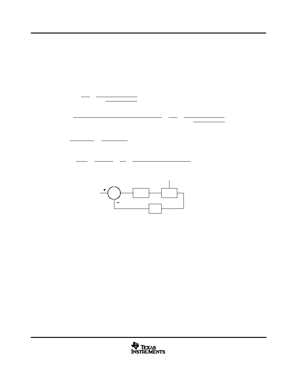
control loop
Figure 12 shows the control block diagram for the typical application shown in Figure 9. G
C
(s) is the
compensation network's transfer function (TF), G
OPTO
(s) is the opto-isolator TF, G
CO
(s) is the control-to-output
TF, and H(s) is the divider TF. The following equations can be used to estimate the frequency response of each
gain block, where f
OPTO_pole
is the frequency, where the optoisolator is ≠3 dB from its dc operating point, and
V
REF_TL431
is the reference voltage of the TL431 shunt regulator. R
LOAD
represents the typical load impedance
for the design.
G
OPTO
(s)
+
R13
R36
1
1
)
s
2
p
f
OPTO_pole
G
C
(s)
+
s
R35
C14
)
1
s
C14
R31
(1
)
(s
R35
C15))
R13
R36
1
1
)
s
2
p
f
OPTO_pole
H(s)
+
R27
R27
)
R31
+
V
VREF_TL431
V
OUT
G
CO
(s)
+
V
OUT
V
C
+
R
LOAD
R
SENSE2
N
P
N
s
1
)
s
C
OUT
ESR
1
)
s
C
OUT
R
LOAD
VREF_TL431
GC(s)
GCO(s)
VBOOST
VOUT
H(s)
VC
Figure 12. UCC38500 Control Block
(38)
(39)
(40)
(41)

UCC28500, UCC28501, UCC28502, UCC28503
UCC38500, UCC38501, UCC38502, UCC38503
SLUS419C ≠ AUGUST 1999 ≠ REVISED NOVEMBER 2001
24
www.ti.com
TYPICAL APPLICATION
Figure 13 shows the circuitry for the voltage feedback loop. D13 is a TL431 shunt regulator that functions as
an operational amplifier, providing feedback control.
V
C
= V
ERR
G
CO(s)
UDG≠01091
R13
PGND2
R27
Q5
D14
R36
R16
D13
R31
H11AV1
3
2
1
4
5
6
U3
SGND
VREF
VBOOST
VOUT
C14
R35
C15
GCO(s)
Figure 13. UCC38500 Feedback Loop
Initially the designer must select the resistor values for the divider gain H(s). Equation (42) is used to determine
resistor size. Selecting R27 to be a standard value of 10-k
requires R31 to be approximately 38.3 k
.
R31
+
R27 V
OUT
*
V
REF
V
REF
It is important to correctly bias the TL431 and the optoisolator for proper operation. Zener diode D14 and a
depletion mode J-FET, Q5, supply the bias voltage for the TL431. Resistors R16 and R13 provide the minimum
bias currents for the TL431 and the optoisolator respectively and can be calculated with the following equations.
Where I
OP(min)
is the minimum optoisolation current, and V
VERR(max)
is the maximum voltage seen at the VERR
pin of the UCC38500. VERR has an internal clamp that limits this pin to 4.5 V. V
F
is the typical forward voltage
of the diode in the opto isolator, and I
TL431(min)
is the minimum cathode current of the TL431. For the
components used in this design example R13 is calculated to be approximately 2.0 k
and R16 was calculated
to be approximately 680
. The optoisolator is configured to have dc gain of approximately 20 dB and the
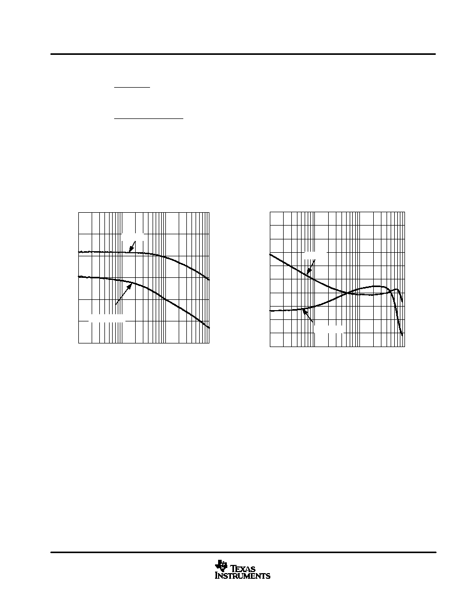
optoisolator ≠3 dB point is approximately 8 kHz. Figure 14 shows the frequency response of the optoisolator.
(42)
UCC28500, UCC28501, UCC28502, UCC28503
UCC38500, UCC38501, UCC38502, UCC38503
SLUS419C ≠ AUGUST 1999 ≠ REVISED NOVEMBER 2001
25
www.ti.com
TYPICAL APPLICATION
R16
+
V
F
I
TL431 (min)
R13
+
V
REF
*
V
VERR (max)
I
OP (min)
To compensate the loop, it is necessary to estimate or measure the control-to-output gain's frequency response
G
CO
(s). The frequency response for G
CO
(s) was measured with a network analyzer and the measured
frequency response is shown in Figure 15.
Figure 14
OPTOISOLATOR TRANSFER FUNCTION
(GAIN AND PHASE)
vs.
FREQUENCY
≠20
0
100
20
≠60
≠40
60
40
60
180
120
0
≠60
≠180
≠120
1 k
10 k
100 k
f ≠ Frequency ≠ Hz
Gain
≠
dB
Phase
≠
Degrees
PHASE
GAIN
Figure 15
100
1 k
10 k
100 k
≠40
≠50
≠20
≠30
0
≠10
20
10
30
50
40
≠144
≠180
≠72
≠108
0
≠36
72
36
108
180
144
Gain
≠
dB
Phase
≠
Degrees
POWER STAGE CONTROL-TO-OUTPUT TRANSFER
FUNCTION (GAIN AND PHASE)
vs.
FREQUENCY
f ≠ Frequency ≠ Hz
GAIN
PHASE
After determining the frequency response of G
CO
(s) it is necessary to define some closed loop frequency
response design goals. The following equation describes the frequency response of the loop gain (T(s)
dB
) of
the system in decibels. Typically, the loop is designed to crossover at a frequency below one-sixth
of the
switching frequency. In order for this design example to have good transient response, the design goal is to have
the loop gain crossover at approximately 1 kHz, which is less than one-sixth of the switching frequency. The
gain crossover frequency for this design example is referenced as f
C
.
T(s) dB
+
G
C
(s)
)
G
CO
(s)
)
H(s)
The compensation network that is used (G
C
(s)) has three poles and one zero. One pole occurs at the origin,
and a second pole is caused by the limitations of the opto-isolator. The third pole is set to attenuate the
high-frequency gain and needs to be set to one-half of the switching frequency. The zero is set at the desired
crossover frequency.
The following equations can be used to select R35, C14 and C15, where G
CO
(s), G
OPTO
(s), and H(s) are the
gains in decibels (dB) of each control block at the desired f
C
. From the graphs in Figures 14 and 15 it can be
observed at the desired crossover frequency G
CO
(s) is approximately 0 dB and G
OPTO
(s) is approximately
(43)
(44)
(45)
UCC28500, UCC28501, UCC28502, UCC28503
UCC38500, UCC38501, UCC38502, UCC38503
SLUS419C ≠ AUGUST 1999 ≠ REVISED NOVEMBER 2001
26
www.ti.com
23 dB. Therefore the compensation circuitry needs to have a gain of ≠23 dB at the desired crossover frequency.
For this example R35 is calculated at approximately 18.2 k
. Capacitor C14 is estimated to be approximately
10 nF and C15 is calculated at approximately 180 pF.
H(s)
+
20 log
V
REF
V
OUT
R35
+
R31
10
*
G
CO
(s) dB
)
G
OPTO
(s) dB
)
H(s) dB
C14
+
1
2
p
R35
f
C
C15
+
1
2
p
R35
f
SW
2
Figure 16 shows the frequency response of the compensation network G
C
(s) and Figure 17 shows the
measured frequency response of the loop gain T(s). The frequency response characteristics in Figure 17 show
that f
C
is approximately 1.5 kHz with a phase margin of about 55 degrees. The gain margin is approximately
50 dB.
Figure 16
FEEDBACK CONTROL TRANSFER FUNCTION
(GAIN AND PHASE)
vs.
FREQUENCY
≠20
0
100
20
≠60
≠40
60
40
60
180
120
0
≠60
≠180
≠120
1 k
10 k
100 k
COMPENSATION
GAIN
COMPENSATION
PHASE
G
OPT
O
≠
Gain
≠
dB
Phase
≠
Degrees
f ≠ Frequency ≠ Hz
≠20
0
20
≠60
≠40
60
40
100
1 k
10 k
100 k
60
180
120
0
≠60
≠180
≠120
Figure 17
G
OPT
O
≠
Gain
≠
dB
Phase
≠
Degrees
TOTAL LOOP TRANSFER FUNCTION
(GAIN AND PHASE)
vs.
FREQUENCY
f ≠ Frequency ≠ Hz
LOOP GAIN
LOOP PHASE
(46)
(47)
(48)
(49)

IMPORTANT NOTICE
Texas Instruments Incorporated and its subsidiaries (TI) reserve the right to make corrections, modifications,
enhancements, improvements, and other changes to its products and services at any time and to discontinue
any product or service without notice. Customers should obtain the latest relevant information before placing
orders and should verify that such information is current and complete. All products are sold subject to TI's terms
and conditions of sale supplied at the time of order acknowledgment.
TI warrants performance of its hardware products to the specifications applicable at the time of sale in
accordance with TI's standard warranty. Testing and other quality control techniques are used to the extent TI
deems necessary to support this warranty. Except where mandated by government requirements, testing of all
parameters of each product is not necessarily performed.
TI assumes no liability for applications assistance or customer product design. Customers are responsible for
their products and applications using TI components. To minimize the risks associated with customer products
and applications, customers should provide adequate design and operating safeguards.
TI does not warrant or represent that any license, either express or implied, is granted under any TI patent right,
copyright, mask work right, or other TI intellectual property right relating to any combination, machine, or process
in which TI products or services are used. Information published by TI regarding third≠party products or services
does not constitute a license from TI to use such products or services or a warranty or endorsement thereof.
Use of such information may require a license from a third party under the patents or other intellectual property
of the third party, or a license from TI under the patents or other intellectual property of TI.
Reproduction of information in TI data books or data sheets is permissible only if reproduction is without
alteration and is accompanied by all associated warranties, conditions, limitations, and notices. Reproduction
of this information with alteration is an unfair and deceptive business practice. TI is not responsible or liable for
such altered documentation.
Resale of TI products or services with statements different from or beyond the parameters stated by TI for that
product or service voids all express and any implied warranties for the associated TI product or service and
is an unfair and deceptive business practice. TI is not responsible or liable for any such statements.
Mailing Address:
Texas Instruments
Post Office Box 655303
Dallas, Texas 75265
Copyright
2003, Texas Instruments Incorporated