 | –≠–ª–µ–∫—Ç—Ä–æ–Ω–Ω—ã–π –∫–æ–º–ø–æ–Ω–µ–Ω—Ç: UCC2857 | –°–∫–∞—á–∞—Ç—å:  PDF PDF  ZIP ZIP |
UCC1857
UCC2857
UCC3857
PRELIMINARY
DESCRIPTION
The UCC3857 provides all of the control functions necessary for an Iso-
lated Boost PFC Converter. These converters have the advantage of trans-
former isolation between primary and secondary, as well as an output bus
voltage that is lower than the input voltage. By providing both power factor
correction and down conversion in a single power processing stage, the
UCC3857 is ideal for applications which require high efficiency, integration,
and performance.
The UCC3857 brings together the control functions and drivers necessary
to generate overlapping drive signals for external IGBT switches, and pro-
vides a separate output to drive an external power MOSFET which pro-
vides zero current switching (ZCS) for both the IGBTs. Full programmability
is provided for the MOSFET driver delay time with an external RC network.
ZCS for the IGBT switches alleviates the undesirable turn off losses typi-
cally associated with these devices. This allows for higher switching fre-
quencies, smaller magnetic components and higher efficiency. The power
factor correction (PFC) portion of the UCC3857 employs the familiar aver-
age current control scheme used in previous Unitrode controllers. Internal
circuitry changes, however, have simplified the design of the PFC section
and improved performance.
(continued)
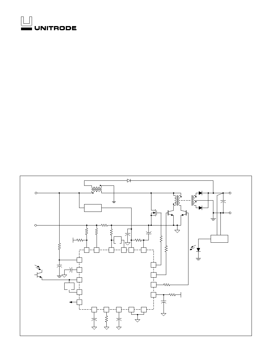
Isolated Boost PFC Preregulator Controller
8
15
4
VD
13
7
3
VIN
CAO
CA≠
MOUT
PKLMT
14
MOSDRV
16
IGDRV1
18
IGDRV2
17
PGND
20
CT
6
AGND
19
RT
20
SS
5
VREF
12
DELAY
11
VAO
10
VA≠
2
CRMS
1
IAC
REF
REF
Z
V
Z
C
R
S
Q2
Q1
T1
FEEDBACK
CKT
OPTO
BIAS
SUPPLY
QA
R
AC
V
OUT
+
≠
RECTIFIED
AC INPUT
REF
UCC3857
C
F
TYPICAL APPLICATION CIRCUIT
FEATURES
∑
PFC With Isolation, V
O
< V
IN
∑
Single Power Stage
∑
Zero Current Switched IGBT
∑
Programmable ZCS Time
∑
Corrects PF to >0.99
∑
Fixed Frequency, Average Current
Control
∑
Improved RMS Feedforward
∑
Soft Start
∑
9V to 18V Supply V Range
∑
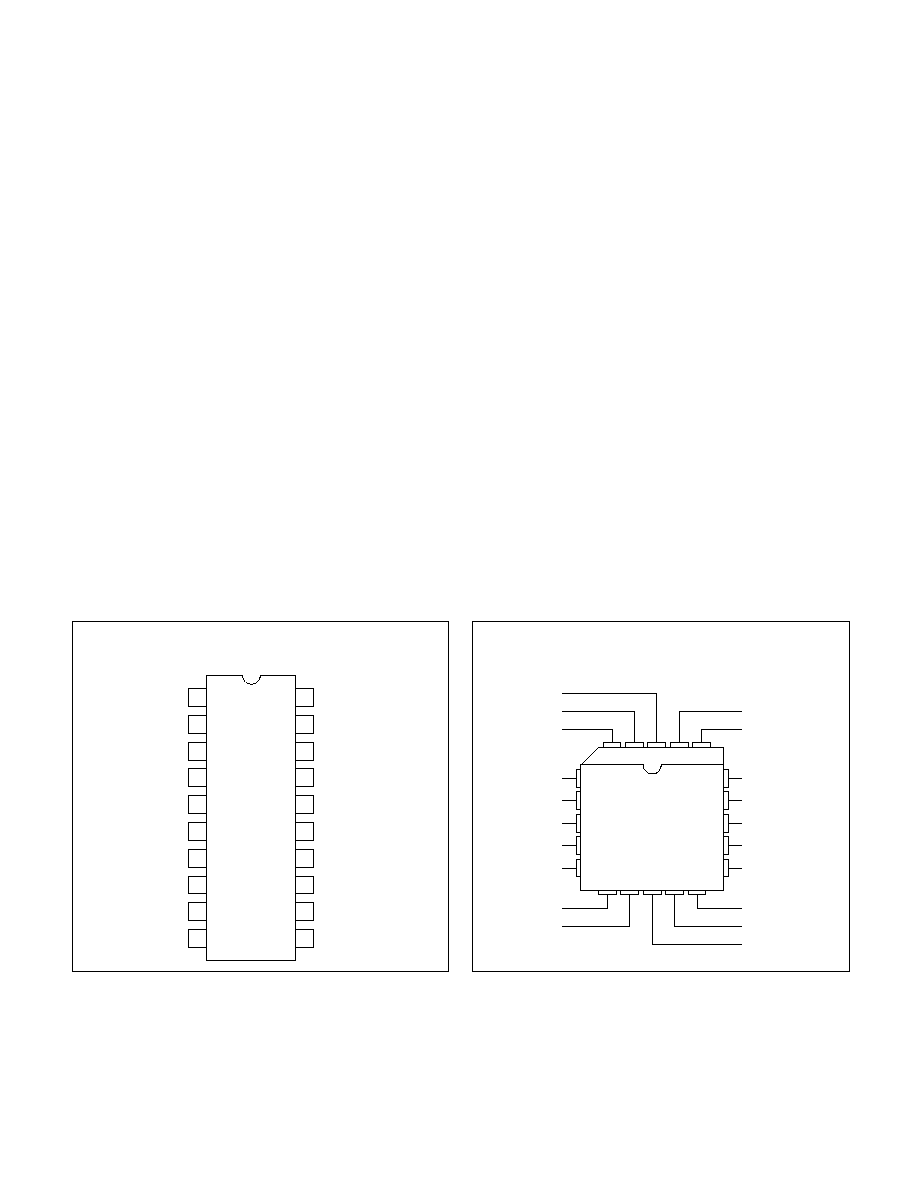
20-Pin DW, N, J, and L Packages
02/99
UDG-98065
2
UCC1857
UCC2857
UCC3857
ABSOLUTE MAXIMUM RATINGS
Input Supply Voltage (VIN, VD) . . . . . . . . . . . . . . . . . . . . . . 18V
General Analog/Logic Inputs
(CRMS, MOUT, CA≠, VA≠, CT, RT, PKLMT)
(Maximum Forced Voltage) . . . . . . . . . . . . . . . . ≠0.3V to 5V
IAC (Maximum Forced Current) . . . . . . . . . . . . . . . . . . . 300
µ
A
Reference Output Current . . . . . . . . . . . . . . . Internally Limited
Output Current (MOSDRV, IGDRV1, IGDRV2)
Pulsed. . . . . . . . . . . . . . . . . . . . . . . . . . . . . . . . . . . . . . . . 1A
Continuous . . . . . . . . . . . . . . . . . . . . . . . . . . . . . . . . 200mA
Storage Temperature . . . . . . . . . . . . . . . . . . .
-
65∞C to +150∞C
Junction Temperature . . . . . . . . . . . . . . . . . . .
-
55∞C to +150∞C
Lead Temperature (Soldering, 10 Sec.). . . . . . . . . . . . . +300∞C
Unless otherwise indicated, voltages are reference to ground
and currents are positive into, negative out of the specified ter-
minal. Pulsed is defined as a less than 10% duty cycle with a
maximum duration of 500 s. Consult Packaging Section of
Databook for thermal limitations and considerations of pack-
ages.
3
18
17
16
IAC
1
2
20 19
15
14
4
5
6
7
8
9
11
10
12 13
CRMS
MOUT
CT
RT
IGDRV2
PGND
IGDRV1
VD
MOSDRV
VIN
VREF
AGND
CA≠
CAO
PKLMT
DELAY
VAO
SS
VA≠
DESCRIPTION (continued)
Controller improvements include an internal 6 bit A-D
converter for RMS input line voltage detection, a zero
load power circuit, and significantly lower quiescent op-
erating current. The A-D converter eliminates an external
2 pole low pass filter for RMS detection.
This simplifies the converter design, eliminates 2nd har-
monic ripple from the feedforward component, and pro-
vides an approximate 6 times improvement in input line
transient response. The zero load power comparator
prevents energy transfer during open load conditions
without compromising power factor at light loads. Low
startup and operating currents which are achieved
through the use of Unitrode's BCDMOS process simplify
the auxiliary bootstrap supply design.
Additional features include: under voltage lockout for reli-
able off-line startup, a programmable over current shut-
down, an auxiliary shutdown port, a precision 7.5V
reference, a high amplitude oscillator ramp for improved
noise immunity, softstart, and a low offset analog square,
multiple and divide circuit. Like previous Unitrode PFC
controllers, worldwide operation without range switches
is easily implemented.
IGDRV2
RT
CT
PGND
IGDRV1
MOSDRV
VD
PKLMT
1
2
3
4
5
6
7
8
20
19
18
17
16
15
14
13
CRMS
IAC
CAO
AGND
CA≠
MOUT
VIN
VREF
9
10
VA≠
SS
DELAY
VAO
12
11
CONNECTION DIAGRAMS
DIL-20, SOIC- 20 (Top View)
J, N and DW Packages
PLCC-20 (Top View)
L Package

3
UCC1857
UCC2857
UCC3857
ELECTRICAL CHARACTERISTICS:
Unless otherwise stated, these specifications apply for T
A
= 0∞C to 70∞C for the
UCC3857, ≠40∞C to +85∞C for the UCC2857, and ≠55∞C to +125∞C for the UCC1857, V
VIN
, V
VD
= 12V, R
T
= 19.2K, C
T
= 680pF.
T
A
= T
J
.
PARAMETER
TEST CONDITIONS
MIN
TYP
MAX
UNITS
Input Supply
Supply Current, Active
No Load on Outputs, V
VD
= V
VIN
3.5
5
mA
Supply Current, Startup
No Load on Outputs, V
VD
= V
VIN
60
TBD
µ
A
VIN UVLO Threshold
13.75
15.5
V
UVLO Threshold Hysteresis
3
3.75
TBD
V
Reference
Output Voltage (V
VREF
)
T
J
= 25∞C, I
REF
= 1mA
7.387
7.5
7.613
V
Over Temperature, UCC3857
7.368
7.5
7.631
V
Over Temperature, UCC1857, UCC2857
7.313
7.5
7.687
V
Load Regulation
I
REF
= 1mA to 10mA
2
10
mV
Line Regulation
V
VIN
= V
VD
= 12V to 16V
2
15
mV
Short Circuit Current
V
VREF
= 0V
≠55
≠30
mA
Current Amplifier
Input Offset Voltage
(Note 1)
≠3
0
3
mV
Input Bias Current
(Note 1)
≠50
nA
Input Offset Current
(Note 1)
25
nA
CMRR
V
CM
= 0V to 1.5V, V
CAO
= 3V
80
dB
AVOL
V
CM
= 0V, V
CAO
= 2V to 5V
65
85
dB
VOH
Load on CAO = 50
µ
A, V
MOUT
= 1V, V
CA≠
= 0V
6
7
V
VOL
Load on CAO = 50
µ
A, V
MOUT
= 0V, V
CA≠
= 1V
0.2
V
Maximum Output Current
Source : V
CA≠
= 0V, V
MOUT
= 1V, V
CAO
= 3V
≠150
µ
A
Sink : V
CA≠
= 1V, V
MOUT
= 0V, V
CAO
= 3V
5
30
50
mA
Gain Bandwidth Product
f
IN
= 100kHz, 10mV p ≠ p
3
5
MHz
Voltage Amplifier
Input Voltage
Measured on V
VA≠,
V
VAO
= 3V
2.9
3
3.1
V
Input Bias Current
Measured on V
VA≠,
V
VAO
= 3V
≠50
nA
AVOL
V
VAO
= 1V to 5V
75
dB
VOH
Load on V
VAO
= ≠50
µ
A, V
VA≠
= 2.8V
5.3
5.55
5.7
V
VOL
Load on V
VAO
= 50
µ
A, V
VA≠
= 3.2V
0.1
0.45
V
Maximum Output Current
Source: V
VA≠
= 2.8V, V
VAO
= 3V
≠20
≠12
≠5
mA
Sink: V
VA≠
= 3.2V, V
VAO
= 3V
5
20
30
mA
Oscillator
Initial Accuracy
T
J
= 25∞C
42.5
50
57.5
kHz
40
50
60
kHz
Voltage Stability
V
VIN
= 12V to 18V
1
%
CT Ramp Peak-Valley Amplitude
4
4.5
5
V
CT Ramp Valley Voltage
1.5
V
Output Drivers
VOH
IL = ≠100mA
9
10
V
VOL
IL = 100mA
0.1
0.5
V
Rise Time
C
LOAD
= 1nF
25
TBD
ns
Fall Time
C
LOAD
= 1nF
10
TBD
ns
Trailing Edge Delay
Delay Time
R
D
= 12k, C
D
= 200pF, V
VAO
= 4V
1.6
2
2.4
µ
s

4
UCC1857
UCC2857
UCC3857
PIN DESCRIPTIONS
AGND: Reference point of the internal reference and all
thresholds, as well as the return for the remainder of the
device except for the output drivers.
CA≠: Inverting input of the inner current loop error ampli-
fier.
CAO: Output of the inner current loop error amplifier.
This output can swing between approximately 0.2V and
6V. It is one of the inputs to the PWM comparator.
VAO: This is the output of the voltage loop error ampli-
fier. It is internally clamped to approximately 5.6V by the
UCC3857 and can swing as low as approximately 0.1V.
Voltages below 0.5V on VAO will disable the MOSDRV
output and force the IGDRV1 and IGDRV2 outputs to a
zero overlap condition.
CRMS: A capacitor is connected between CRMS and
ground to average the AC line voltage over a half cycle.
CRMS is internally connected to the RMS detection cir-
cuitry.
CT: A capacitor (low ESR, ESL) is tied between CT and
ground to set the ramp generator switching frequency in
conjunction with RT. The ramp generator frequency is ap-
proximately given by:
f
R
C
SW
T
T
0.67
∑
.
DELAY: A resistor to VREF and a capacitor to AGND are
connected to DELAY to set the overlap delay time for the
MOSDRV output stage. The overlap delay function can
be disabled by removing the capacitor to AGND.
IAC: A resistor is connected to the rectified AC input line
voltage from IAC. This provides the internal multiplier
and the RMS detector with instantaneous line voltage in-
formation.
IGDRV1: Driver output for one of the two external IGBT
power switches.
IGDRV2: Driver output for one of the two external IGBT
power switches.
MOSDRV: Driver output for the external power MOSFET
switch.
MOUT: Output of the analog multiply and divide circuit.
The output current from MOUT is fed into a resistor to
the return leg of the input bridge. The resultant waveform
forms the sine reference for the current error amplifier.
PKLMT: Inverting input of the peak current limit com-
parator. The threshold for this comparator is nominally
set to 0V. The peak limit comparator terminates the
MOSDRV, IGDRV1 and IGDRV2 outputs when tripped.
PGND: Return for all high level currents, internally tied to
the output driver stages of the UCC3857.
RT: A resistor, R
T
is tied between RT and ground to set
the charging current for the internal ramp generator. The
UCC3857 provides a temperature compensated 3.0V at
RT. The oscillator charging current is therefore: 3.0V/R
T
.
Current out of RT should be limited to 250
µ
A for best
performance.
VA≠: This is the feedback input for the outer voltage con-
trol loop. An external opto isolator circuit provides the
ELECTRICAL CHARACTERISTICS:
Unless otherwise stated, these specifications apply for T
A
= 0∞C to 70∞C for the
UCC3857, ≠40∞C to +85∞C for the UCC2857, and ≠55∞C to +125∞C for the UCC1857, V
VIN
, V
VD
= 12V, R
T
= 19.2K, C
T
= 680pF.
T
A
= T
J
.
PARAMETER
TEST CONDITIONS
MIN
TYP
MAX
UNITS
Soft Start
Charge Current
10
µ
A
Shutdown Comparator Threshold
Measured on SS
0
0.4
V
Multiplier
Output Current, IAC Limited
I
AC
= 100
µ
A, V
VAO
= 5.5V, V
CRMS
= 0V
≠200
µ
A
Output Current, Power Limited
I
AC
= 100
µ
A, V
VAO
= 5.5V, V
CRMS
= 1V
≠200
µ
A
Output Current, Zero
I
AC
= 0
≠2
0
2
µ
A
Gain Constant
2.5
1/V
Zero Power, Peak Current
Zero Power Comparator Threshold
Measured on VAO
0.5
V
Peak Current Limit Comparator
Threshold
Measured on PKLMT
0
V
Note 1: Common mode voltages = 0V, V
CAO
= 3V
5
UCC1857
UCC2857
UCC3857
output voltage regulation information to VA≠ across the
isolation barrier.
SS: A capacitor is connected between SS and GND to
provide the UCC3857 soft start feature. The voltage on
VAO, is clamped to approximately the same voltage as
SS. An internal 10
µ
A (nominal) current source is pro-
vided by the UCC3857 to charge the soft start capacitor.
VD: Positive supply rail for the three output driver stages.
The voltage applied to VD must be limited to less than
18VDC. VD should be bypassed to PGND with a 0.1
µ
F
to 1.0
µ
F low ESR, ESL capacitor for best results. VD and
VIN can be isolated from each other with an RC lowpass
filter for better supply noise rejection.
VIN: Input voltage supply to the UCC3857. This voltage
must be limited to less than 18VDC. The UCC3857 is en-
abled when the voltage on VIN exceeds 13.75V (nomi-
nal).
VREF: Output of the precision 7.5V reference. A 0.01
µ
F
to 0.1
µ
F low ESR, ESL bypass capacitor is recom-
mended between VREF and AGND for best perform-
ance.
PIN DESCRIPTIONS (continued)
V
CT
(PIN 20) &
V
CAO
(PIN 8)
CLOCK
(INTERNAL)
TOGGLE F/F Q
(INTERNAL)
IGDRV1
(PIN 16)
IGDRV2
(PIN 18)
MOSDRV
(PIN 14)
TD1
Figure 1. Typical control circuit timing diagram.
UDG-98217
APPLICATION INFORMATION
UCC3857 is designed to provide a solution for single
stage power factor correction and step-down or step-up
function, using an isolated boost converter. The Typical
Application Circuit shows the implementation of a typical
isolated boost converter using IGBTs as main switches in
push-pull configuration and using a MOSFET as an auxil-
iary switch to accomplish soft-switching of IGBTs. Many
variations of this implementation are possible including
bridge-type circuits. The presense of low frequency ripple
on the output makes this approach practical for distrib-
uted bus applications. It will not provide the highly regu-
lated low ripple outputs typically required by logic level
supplies.
The circuit shown in the Typical Application Circuit pro-
vides several advantages over a more conventional ap-
proach of deriving a DC bus voltage from AC line with
power factor correction. The conventional approach uses
two power conversion stages and has higher cost and
complexity. With the use of UCC3857, the dual function-
ality of power factor correction and voltage step-down is
combined into a single stage.
The power stage comprises a current-fed push-pull con-
verter where the ON times of the push-pull switches (Q1
and Q2) are overlapped to provide effective duty cycle of
a conventional PWM boost converter.
When only one
switch is on, the power is transferred to the output
6
UCC1857
UCC2857
UCC3857
4
2
1
12
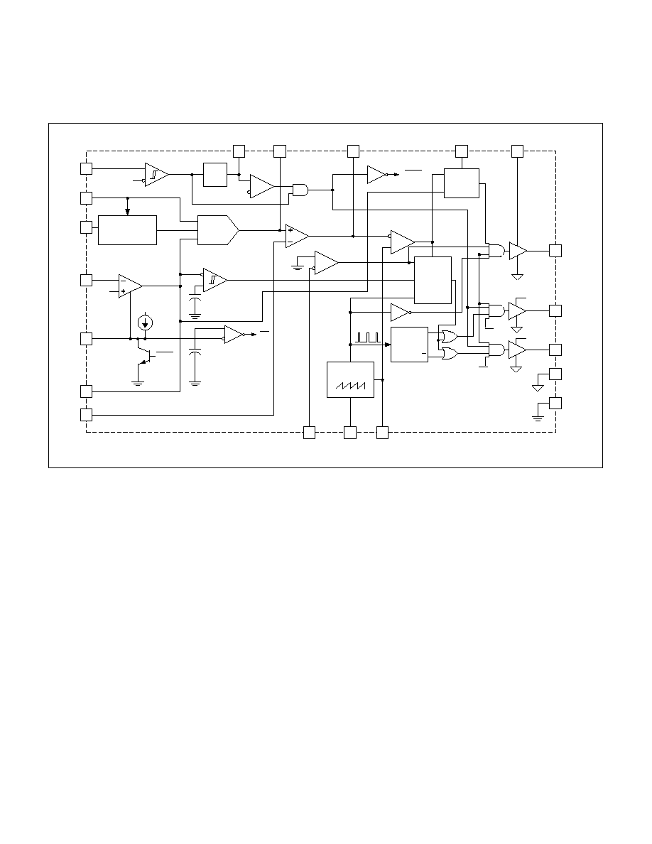
VIN
IAC
UVLO
13.75V / 10V
CRMS
RMS DETECT
AND
CONDITIONING
X
˜
X
MULT
10
VA≠
3.0V
0.5V
ZERO POWER
9
SS
10
µ
A
11
VAO
7
CA≠
ENBL
1.0V
ALWAYS
ON
SD
7.5V
REF
VREF
5
REF GOOD
3
ENBL
VOLTAGE AMP
13
PKLMT
CURRENT AMP
PEAK LIMIT
COMP
8
MOUT
CAO
20
CT
19
RT
OSCILLATOR
TOGGLE
F/F
Q
Q
PWM
LATCH
Q
R
R
S
R
PWM
COMP
SD
SD
TRAILING
EDGE
DELAY
DELAY
15
VD
14
MOSDRV
16
IGDRV1
18
IGDRV2
17 PGND
6
AGND
DRIVER
DRIVER
DRIVER
VD
VD
APPLICATION INFORMATION (continued)
BLOCK DIAGRAM
through the transformer and the output rectifier. It can
be seen that the∏
˜
operation on the primary side of the
circuit is that of a boost converter and UCC3857 pro-
vides input current programming using average current
mode control to achieve unity power factor. The trans-
former turns ratio can be used to get the required level
of output voltage (higher or lower than the peak line volt-
age). The transformer also provides galvanic isolation
for the output voltage.
Power stage optimization involves design and selection
of components to meet the performance and cost objec-
tives.
These include the power switches, transformer
and inductor design.
The choice of IGBTs is based on their advantage over
MOSFETs at higher voltages. For universal line opera-
tion, the voltage stress on the push-pull switches can
approach 1000V. However, the slow turn-off of IGBTs
can contribute high switching losses and the use of
MOSFET (QA) helps turn the IGBTs off with zero voltage
across them (ZCS turn-off). This is accomplished by
keeping QA on (beyond the turn-off of Q1 or Q2 ≠ see
Fig. 1 for waveforms) to allow the inductor current to di-
vert from IGBT to MOSFET while the IGBT is turning off
and still maintain zero volts. The MOSFET delay time
(TD1) effectively adds to the boost inductor charge pe-
riod. The voltage stress of the MOSFET is half the stress
of the IGBTs under normal operating conditions. How-
ever, QA can see much higher voltage stress under
start-up and short circuit conditions as the converter oper-
ates in a flyback mode then. For different operating re-
quirements or constraints (e.g. single North American line
operation), the choice of switching components may be
different (e.g. MOSFETs for Q1 and Q2 and no QA) as
the voltage stress is different. In that case, UCC3857 can
still be used without using the MOSDRV output.
Transformer design is very critical in this topology. The
push-pull transformer must have minimal leakage induc-
tance between the primary and secondary windings. Simi-
larly, the leakage between the two primary windings must
be minimized. In practice, it is hard to achieve both tar-
gets without using sophisticated construction techniques
such as interleaving, use of foils etc. In many cases, it
may be beneficial to use a planar transformer to achieve
these objectives. The effects of higher leakage induc-
tance include higher voltage stresses, ringing, power
losses and loss of available duty cycle. The high voltage
levels make it difficult to design effective snubber circuits
for this leakage induced ringing.
UDG-98218

7
UCC1857
UCC2857
UCC3857
The design of the boost inductor is very similar to the
conventional boost converter. However, as shown in the
Typical Application Circuit, an additional winding con-
nected to the output through a diode is required on the
boost inductor. This winding must have the same turns
ratio as the transformer and meet the isolation require-
ments. This winding is required to provide a discharge
path for the inductor energy when the push-pull switches
are both off. During start-up, when the output voltage is
zero, the converter can see very high inrush currents.
The overcurrent protection circuit of UCC3857 will shut
down all the outputs when the set threshold is crossed.
At that instance, the boost inductor auxiliary winding di-
rects the energy to the output. This is a preferred manner
of bringing the output voltage up to prevent the main
switches from handling the high levels of inrush current.
However, when the auxiliary winding is transferring the
power to the output, the voltage stress across QA be-
comes input voltage plus the reflected output volt-
age≠higher than its steady state value of reflected output
voltage.
Chip Bias Supply and Start-up
UCC3857 is implemented using Unitrode's BCDMOS
process which allows minimization of the start-up (60 A
typical) and operating (3.5mA typical) supply currents. It
results in significantly lower power consumption in the
trickle charge resistor used to start-up the IC.
Oscillator Set-up
The oscillator of UCC3857 is designed to have a wide
ramp amplitude (4.5V p≠p) for higher noise immunity.
The CT pin has the sawtooth waveshape and during the
discharge time of C
T
, a clock pulse is generated. During
the discharge period, the effective internal impedance to
GND is 600 . Based on this, the discharge time is given
by 831
∑
C
T
. As shown in the waveforms of Fig. 1, the in-
ternal clock pulse width is equal to the discharge time
and that sets the minimum dead time between IGDRV1
and IGDRV2. The clock frequency is given by
f
R
C
R
C
SW
T
T
T
T
=
∑
+
∑
∑
∑
1
1 5
831
1
1 5
( .
)
( .
)
(1)
The IGDRV1 and IGDRV2 outputs are switched at half
the clock frequency while MOSDRV is switched at the
clock frequency.
Reference Signal (I
MULT
) generation
Like the UC3854 series, the UCC3857 has an analog
computation unit (ACU) which generates a reference cur-
rent signal for the current error amplifier. The inputs to
the ACU are signals proportional to instantaneous line
voltage, input voltage RMS information and the voltage
error amplifier output. Unlike prior techniques of RMS
voltage sensing, UCC3857 employs a patent pending
technique to simplify the RMS voltage generation and
eliminate
performance
degradation
caused
by
the
previous techniques. With the novel technique (shown in
Fig. 3), need for external 2-pole filter for V
RMS
generation
is eliminated. Instead, the IAC current is mirrored and
used to charge an external capacitor (C
CRMS
) during a
half cycle. The voltage on CRMS takes the integrated si-
nusoidal shape and is given by equation 2. At the end of
the half-cycle, CRMS voltage is held and converted into
a 6-bit digital word for further processing in the ACU.
C
CRMS
is discharged and readied for integration during
next half cycle.
The advantage of this method is that the second har-
monic ripple on the V
RMS
signal is virtually eliminated.
Such second harmonic ripple is unavoidable with the lim-
ited roll-off of a conventional 2-pole filter and results in
3rd harmonic distortion in the input current signal. The
dynamic response to the input line variations is also im-
proved as a new V
RMS
signal is generated every cycle.
(
)
V
I
pk
C
t
CRMS
AC
CRMS
=
∑ ∑
-
(
)
cos
2
1
(2)
V
pk
I
pk
C
CRMS
AC
CRMS
(
)
(
)
=
∑
(2a)
For proper operation, I
AC
(pk) should be selected to be
100 A at peak line voltage. For universal input voltage
with peak value of 265 VAC, this means R
AC
= 3.6M. The
noise sensitivity of the IC requires a small bypass capaci-
tor for high frequency noise filtering. The value of this ca-
pacitor should be limited to 220nF maximum. The V
CRMS
value should be approximately 1V at the peak of low line
(80 VAC) to minimize any digitization errors. The peak
value of V
CRMS
at high line then becomes 3.5V. The de-
sired C
CRMS
can be calculated from equation 2 to be
75nF for 60Hz line.
The multiplier output current is given by equation (3) with
K = 0.33.
I
V
I
K
V
MULT
VAO
AC
CRMS
=
∑
∑
(
≠ . )
0 5
2
(3)
The multiplier peak current is limited to 200 A and the
selected values for I
AC
and V
CRMS
should ensure that
the current is within this range. Another limitation of the
multiplier is that I
MULT
can not exceed two times the IAC
current, limiting the minimum voltage on V
CRMS
.
The discrete nature of the RMS voltage feedforward
means that there are regions of operation where the in-
APPLICATION INFORMATION (cont.)

8
UCC1857
UCC2857
UCC3857
put voltage changes, but the V
RMS
value fed into the
multiplier does not change. The voltage error amplifier
compensates for this by changing its output to maintain
the required multiplier output current. When the output of
the ADC changes, there is a jump in the output of the er-
ror amplifier. This has minimal impact on the overall con-
verter operation.
Another key consideration with the RMS voltage scheme
is that it relies on the zero-crossing of the Iac signal to be
effective. At very light loads and high line conditions, the
rectified AC does not quite reach zero if a large capacitor
is being used for filtering on the rectified side of the
bridge. In such instances, the feedforward effect does
not take place and the controller functionality is compro-
mised. For UCC3857, the I
AC
current should go below
10 A for the zero crossing detection to take place. It is
recommended that the capacitor value be kept low
enough for light load operation or that the alternative
scheme shown in Fig. 4 be used for I
AC
sense.
Gate Drive Considerations
The gate drive circuits in UCC3857 are designed for high
speed driving of the power switches. Each drive circuit
consists of low impedance pull-up and pull-down DMOS
output stages. The UCC3857 provides separate supply
and ground pins (VD and PGND) for the driver stages.
These pins allow better local bypassing of the driver cir-
cuits. VD can also be used to ensure that the SOA limits
of the output stages are not violated when driving high
peak current levels. For this, VD can be kept as low as
possible (e.g. 10V) while VIN can go higher to handle the
UVLO requirements.
Current Amplifier Set-up
Once the multiplier is set-up by choosing the V
RMS
range, the current amplifier components can be de-
signed. The maximum multiplier output is at low line, full
load conditions. The inductor peak current also occurs at
the same point. The multiplier terminating resistor can be
determined using equation 4.
A
D
MULTI
DAC
6 BIT
WORD
REGISTER
A
B
C
A
∑
B
C
VAO
IAC
R
AC
1
2
(X
2
)
C
CRMS
CRMS
Figure 3. Novel RMS voltage generation scheme.
APPLICATION INFORMATION (cont.)
1
IAC
UCC3857
R
AC
BRIDGE
RECTIFIER
AC LINE
Figure 4. Alternative implementation for sensing I
AC
.

9
UCC1857
UCC2857
UCC3857
UNITRODE CORPORATION
7 CONTINENTAL BLVD. ∑ MERRIMACK, NH 03054
TEL. (603) 424-2410
©
FAX (603) 424-3460
R
I
R
I
MULT
L PK
SENSE
MULT PK
=
∑
-
-
(4)
The current amplifier can be compensated using a previ-
ously presented techniques (U-134) summarized here. A
simplified high frequency model for inductor current to
duty cycle transfer function is given by
G
s
i
d
Vo
L
id
L
S
( )
=
=
(5)
The gain of the current feedback path at the frequency of
interest (crossover) is given by
d
i
R
R
R
V
L
SENSE
Z
I
SE
=
∑
∑
1
(6)
Where VSE is the ramp amplitude (p-p) which is 4.5V for
UCC3857. Combining equations. 5 and 6 yields the loop
gain of the current loop and equating it to 1 at the de-
sired crossover frequency can result in a design value for
R
Z
. The current loop crossover frequency should be lim-
ited to about 1/3 of the switching frequency of the con-
verter to ensure stability. See Unitrode Application Note
U-140 for further information.
Trailing Edge Delay
As shown in the waveforms of Fig. 1, the modified iso-
lated boost converter requires drive signals for the two
main (IGBT) switches and the auxiliary (MOSFET) switch
with certain timing relationships. The delay between
turn-off of an IGBT and turn-off of the MOSFET can be
programmed for the UCC1857. In a PFC application, the
input line varies from zero to the AC peak level, resulting
in a wide range of required duty ratios.
A fixed delay
time will induce line current distortion at the peaks of the
AC line under high line and/or light load conditions. This
is caused by the minimum controllable duty ratio im-
posed on the modulator by the fixed delay. If the mini-
mum controllable duty ratio is fixed, the inner current
loop can exhibit a limit cycle oscillation at the line peaks,
inducing line current distortion.
The UCC1857 has an adaptive MOSFET delay genera-
tor, which is directly modulated by load power demand.
Referring to Fig. 5, this circuit directly varies the delay
time based on the output level of the voltage error ampli-
fier, which in an average current mode PFC converter
with line feedforward is indicative of load power. The de-
lay time is programmed with external components, R
D
and C
D
. The sequence of events starts when the inter-
nal CLK signal resets latch U2, causing PWMDEL to go
high and the Q output to go low. C
D
was discharged via
M1 and is held low until the internal PWM signal goes
low (indicating turn-off of either of the IGBT drives). At
this point M1 turns off and C
D
charges towards the 7.5V
reference through R
D
. A comparator U1 compares this
voltage to the voltage error amplifier output (V
VAO).
When
the voltage on C
D
is greater than V
VAO
, the latch U2 is
set causing PWMDEL to go low. PWMDEL is logically
ANDed with CLK to produce the signal which commands
the MOSFET driver output (MOSDRV). The delay time,
TD1, is given by
TD
R
C
n
V
D
D
VAO
1
7 5
7 5
=
∑
∑
≠
. ≠
.
(7)
This technique reduces the overlap delay at light loads or
high lines, but maintains a longer delay when the line
voltage is low or the load is heavy. This by definition re-
duces the minimum controllable duty ratio to an accept-
able level, and is programmable by the user. Reducing
the delay time under light current conditions is accept-
able since the IGBT current is directly proportional to
load current. By providing programming flexibility with R
D
and C
D
, the delay times can be optimized for current and
future classes of IGBT switches. The delay can also be
set to zero by removing C
D
from the circuit.
PWM
PWMDEL
CLK
VAO
12
DELAY
C
D
R
D
7.5V REF
CLK
MOSDRV
U2
S
R
Q
Q
Figure 5. Circuit for adaptive MOSFET delay
generation.

IMPORTANT NOTICE
Texas Instruments and its subsidiaries (TI) reserve the right to make changes to their products or to discontinue
any product or service without notice, and advise customers to obtain the latest version of relevant information
to verify, before placing orders, that information being relied on is current and complete. All products are sold
subject to the terms and conditions of sale supplied at the time of order acknowledgement, including those
pertaining to warranty, patent infringement, and limitation of liability.
TI warrants performance of its semiconductor products to the specifications applicable at the time of sale in
accordance with TI's standard warranty. Testing and other quality control techniques are utilized to the extent
TI deems necessary to support this warranty. Specific testing of all parameters of each device is not necessarily
performed, except those mandated by government requirements.
CERTAIN APPLICATIONS USING SEMICONDUCTOR PRODUCTS MAY INVOLVE POTENTIAL RISKS OF
DEATH, PERSONAL INJURY, OR SEVERE PROPERTY OR ENVIRONMENTAL DAMAGE ("CRITICAL
APPLICATIONS"). TI SEMICONDUCTOR PRODUCTS ARE NOT DESIGNED, AUTHORIZED, OR
WARRANTED TO BE SUITABLE FOR USE IN LIFE-SUPPORT DEVICES OR SYSTEMS OR OTHER
CRITICAL APPLICATIONS. INCLUSION OF TI PRODUCTS IN SUCH APPLICATIONS IS UNDERSTOOD TO
BE FULLY AT THE CUSTOMER'S RISK.
In order to minimize risks associated with the customer's applications, adequate design and operating
safeguards must be provided by the customer to minimize inherent or procedural hazards.
TI assumes no liability for applications assistance or customer product design. TI does not warrant or represent
that any license, either express or implied, is granted under any patent right, copyright, mask work right, or other
intellectual property right of TI covering or relating to any combination, machine, or process in which such
semiconductor products or services might be or are used. TI's publication of information regarding any third
party's products or services does not constitute TI's approval, warranty or endorsement thereof.
Copyright
©
1999, Texas Instruments Incorporated