 | –≠–ª–µ–∫—Ç—Ä–æ–Ω–Ω—ã–π –∫–æ–º–ø–æ–Ω–µ–Ω—Ç: UCC2889D | –°–∫–∞—á–∞—Ç—å:  PDF PDF  ZIP ZIP |
Document Outline
- Application Notes
- Design Notes
Off-line Power Supply Controller
∑
Transformerless Off-line
Applications
∑
Ideal Primary-side Bias Supply
∑
Efficient BiCMOS Design
∑
Wide Input Range
∑
Fixed or Adjustable
Low Voltage Output
∑
Uses Low Cost SMD Inductors
∑
Short Circuit Protected
∑
Optional Isolation Capability
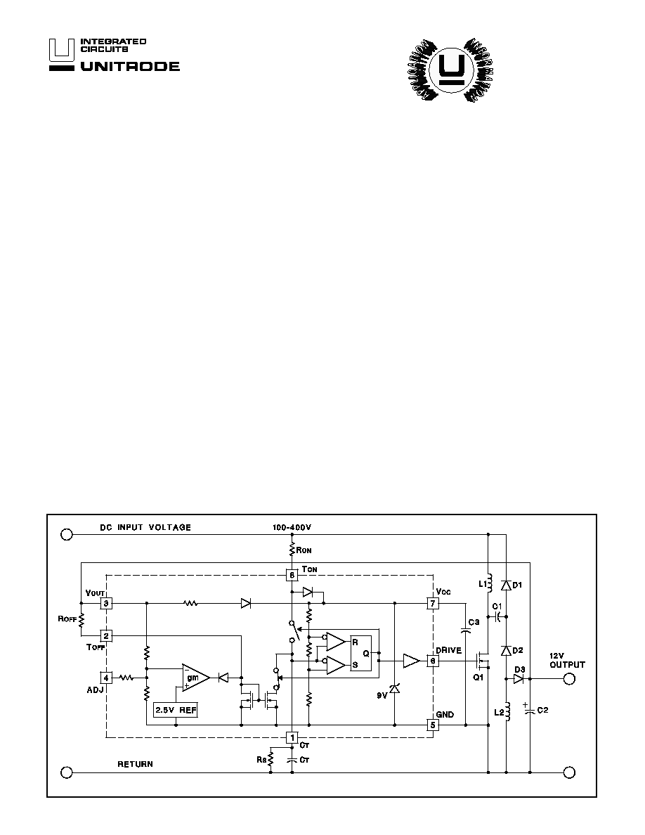
The UCC1889 controller is optimized for use as an off-line, low power, low voltage,
regulated bias supply. The unique circuit topology utilized in this device can be
visualized as two cascaded flyback converters, each operating in the discontinu-
ous mode, and both driven from a single external power switch. The significant
benefit of this approach is the ability to achieve voltage conversion ratios of 400V
to 12V with no transformer and low internal losses.
The control algorithm utilized by the UCC1889 is to force the switch on time to be
inversely proportional to the input line voltage while the switch off time is made in-
versely proportional to the output voltage. This action is automatically controlled by
an internal feedback loop and reference. The cascaded configuration allows a volt-
age conversion from 400V to 12V to be achieved with a switch duty cycle greater
than 10%. This topology also offers inherent short circuit protection since as the
output voltage falls to zero, the switch off time approaches infinity.
The output voltage can be easily set to 12V or 18V. Moreover, it can be pro-
grammed for other output voltages less than 18V with a few additional compo-
nents. An isolated version can be achieved with this topology as described further
in Unitrode Application Note U-149.
UCC1889
UCC2889
UCC3889
SLUS158A - FEBRUARY 1995 - REVISED FEBRUARY 2003
FEATURES
DESCRIPTION
OPERATION
With reference to the application diagram below, when input voltage is first applied,
the R
ON
current into T
ON
is directed to V
CC
where it charges the external capacitor,
C3, connected to V
CC
. As voltage builds on V
CC
, an internal undervoltage lockout
holds the circuit off and the output at DRIVE low until V
CC
reaches 8.4V. At this
time, DRIVE goes high turning on the power switch, Q1, and redirecting the current
into T
ON
to the timing capacitor, C
T
. C
T
charges to a fixed threshold with a current
I
CHG
=0.8
∑
(V
IN
- 4.5V)/R
ON
. Since DRIVE will only be high for as long as C
T
charges, the power switch on time will be inversely proportional to line voltage.
This provides a constant line voltage-switch on time product.
Note: This device incorporates patented technology used under license from Lambda Electronics, Inc.
TYPICAL APPLICATION
UDG-93060-1

UCC1889
UCC2889
UCC3889
OPERATION (cont.)
At the end of the on time, Q1 is turned off and the R
ON
current into T
ON
is again diverted to V
CC
. Thus the cur-
rent through R
ON
, which charges C
T
during the on time,
contributes to supplying control power during the off time.
The power switch off time is controlled by the discharge
of C
T
which, in turn, is programmed by the regulated out-
put voltage. The relationship between C
T
discharge cur-
rent, I
DCHG
, and output voltage is illustrated as follows:
1. When V
OUT
= 0, the off time is infinite. This feature
provides inherent short circuit protection. However, to
ensure output voltage startup when the output is not a
short, a high value resistor, R
S
, is placed in parallel
with C
T
to establish a minimum switching frequency.
2. As V
OUT
rises above approximately 0.7V to its regu-
lated value, I
DCHG
is defined by R
OFF
, and therefore is
equal to:
I
DCHG
= (V
OUT
- 0.7V) / R
OFF
As V
OUT
increases, I
DCHG
increases resulting in the
reduction of off time. The frequency of operation in-
creases and V
OUT
rises quickly to its regulated value.
3. In this region, a transconductance amplifier reduces
I
DCHG
in order to maintain V
OUT
in regulation.
4. If V
OUT
should rise above its regulation range, I
DCHG
falls to zero and the circuit returns to the minimum fre-
quency established by R
S
and C
T
.
The range of switching frequencies is established by
R
ON
, R
OFF
, R
S
, and C
T
as follows:
Frequency = 1/(T
ON
+ T
OFF
)
T
ON
= R
ON
∑
C
T
∑
4.6
V/(V
IN
- 4.5V)
T
OFF
(max) = 1.4
∑
R
S
∑
C
T
Regions 1 and 4
T
OFF
= R
OFF
∑
C
T
∑
3.7V /(V
OUT
- 0.7V)
Region 2, excluding the effects of R
S
which have a minimal impact on T
OFF
.
The above equations assume that V
CC
equals 9V. The
voltage at T
ON
increases from approximately 2.5V to
6.5V while C
T
is charging. To take this into account, V
IN
is adjusted by 4.5V in the calculation of T
ON
. The voltage
at T
OFF
is approximately 0.7V.
DESIGN EXAMPLE
The UCC3889 regulates a 12 volt, 1 Watt nonisolated DC output from AC inputs between 80 and 265 volts. In this ex-
ample, the IC is programmed to deliver a maximum on time gate drive pulse width of 2.4 microseconds which occurs
at 80 VAC. The corresponding switching frequency is approximately 100kHz at low line, and overall efficiency is ap-
proximately 50%. Additional design information is available in Unitrode Application Note U-149.
UDG-93062-3
2

PARAMETER
TEST CONDITIONS
MIN
TYP
MAX
UNITS
General
V
CC
Zener Voltage
I
CC
< 1.5mA
8.6
9.0
9.3
V
Startup Current
V
OUT
= 0
150
250
µ
A
Operating Current I(V
OUT)
V
OUT
= 11V, F = 150kHz
1.2
2.5
mA
Under-Voltage-Lockout
Start Threshold
V
OUT
= 0
8.0
8.4
8.8
V
Minimum Operating Voltage after Start
V
OUT
= 0
6.0
6.3
6.6
V
Hysteresis
V
OUT
= 0
1.8
V
Oscillator
Amplitude
V
CC
= 9V
3.5
3.7
3.9
V
C
T
to DRIVE high Propagation Delay
Overdrive = 0.2V
100
200
ns
C
T
to DRIVE low Propagation Delay
Overdrive = 0.2V
50
100
ns
Driver
VOL
I = 20mA, V
CC
= 9V
0.15
0.4
V
I = 100mA, V
CC
= 9V
0.7
1.8
V
VOH
I =
-
20mA, V
CC
= 9V
8.5
8.8
V
I =
-
100mA, V
CC
= 9V
6.1
7.8
V
Rise Time
C
LOAD
= 1nF
35
70
ns
Fall Time
C
LOAD
= 1nF
30
60
ns
Line Voltage Detection
Charge Coefficient: I
CHG
/ I(T
ON
)
VCT = 3V, DRIVE = High, I(T
ON
) = 1mA
0.73
0.79
0.85
Minimum Line Voltage for Fault
R
ON
= 330k
60
80
100
V
Minimum Current I(T
ON
) for Fault
R
ON
= 330k
220
µ
A
On Time During Fault
C
T
= 150pF, V
LINE
= Min
-
1V
2
µ
s
Oscillator Restart Delay after Fault
0.5
ms
V
OUT
Error Amp
V
OUT
Regulated 12V (ADJ Open)
V
CC
= 9V, I
DCHG
= I(T
OFF
)/2
11.2
11.9
12.8 V
V
OUT
Regulated 18V (ADJ = 0V)
V
CC
= 9V, I
DCHG
= I(T
OFF
)/2
16.5
17.5
19.5 V
Discharge Ratio: I
DCHG
/ I(T
OFF
)
I(T
OFF
) = 50
µ
A
0.9
3
1.0
0
1.07
Voltage at T
OFF
I(T
OFF
) = 50
µ
A
0.6
0.95
1.3
V
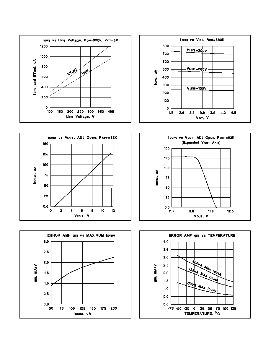
Regulation gm (Note 1)
Max I
DCHG
= 50
µ
A
1.0
mA/V
Max I
DCHG
= 125
µ
A
0.8
1.7
2.9
mA/V
Unless otherwise stated, these specifications hold for T
A
= 0
∞
C to 70
∞
C for the
UCC3889, -40
∞
C
to
+85
∞
C for the UCC2889, and -55
∞
C to +125
∞
C for the UCC1889.
No load at DRIVE pin (C
LOAD
=0).
ELECTRICAL CHARACTERISTICS
DIL-8, SOIC-8 (Top View)
N or J, D Package
CONNECTION DIAGRAM
I
CC
. . . . . . . . . . . . . . . . . . . . . . . . . . . . . . . . . . . . . . . . . . . . 5mA
Current into T
ON
Pin . . . . . . . . . . . . . . . . . . . . . . . . . . . . . 1.5mA
Voltage on V
OUT
Pin . . . . . . . . . . . . . . . . . . . . . . . . . . . . . . . 20V
Current into T
OFF
Pin . . . . . . . . . . . . . . . . . . . . . . . . . . . . 250
µ
A
Storage Temperature . . . . . . . . . . . . . . . . . . . . -65
∞
C to +150
∞
C
Note: Unless otherwise indicated, voltages are referenced to
ground and currents are positive into, negative out of, the speci-
fied terminals.
ABSOLUTE MAXIMUM RATINGS
UCC1889
UCC2889
UCC3889
Note 1: gm is defined as
I
DCHG
V
OUT
for the values of V
OUT
when V
OUT
is in regulation. The two points used to calculate gm are for
I
DCHG
at 65% and 35% of its maximum value.
3
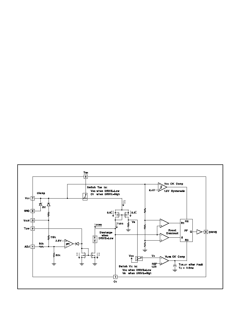
ADJ: The ADJ pin is used to provide a 12V or an 18V
regulated supply without additional external components.
To select the 12V option, ADJ pin is left open. To select
the 18V option, ADJ pin must be grounded. For other out-
put voltages less than 18V, a resistor divider between
V
OUT
, ADJ and GND is needed. Note, however, that for
output voltages less than V
CC
, the device needs addi-
tional bootstrapping to V
CC
from an external source such
as the line voltage. If so, precautions must be taken to
ensure that total I
CC
does not exceed 5mA.
C
T
(timing capacitor): The signal voltage across C
T
has
a peak-to-peak swing of 3.7V for 9V V
CC
. As the voltage
on C
T
crosses the oscillator upper threshold, DRIVE goes
low. As the voltage on C
T
crosses the oscillator lower
threshold, DRIVE goes high.
DRIVE: This output is a CMOS stage capable of sinking
200mA peak and sourcing 150mA peak. The output volt-
age swing is 0 to V
CC
.
GND (chip ground): All voltages are measured with re-
spect to GND.
T
OFF
(regulated output control): T
OFF
sets the dis-
charge current of the timing capacitor through an external
resistor connected between V
OUT
and T
OFF
.
T
ON
(line voltage control): T
ON
serves three functions.
When C
T
is discharging (off time), the current through
T
ON
is routed to V
CC.
When C
T
is charging (on time), the
current through T
ON
is split 80% to set the C
T
charge
time and 20% to sense minimum line voltage which oc-
curs for a T
ON
current of 220
µ
A. For a minimum line volt-
age of 80V, R
ON
is 330k
.
The C
T
voltage slightly affects the value of the charge
current during the on time. During this time, the voltage at
the T
ON
pin increases from approximately 2.5V to 6.5V.
V
CC
(chip supply voltage): The supply voltage of the
device at pin V
CC
is internally clamped at 9V. Normally,
V
CC
is not directly powered from an external voltage
source such as the line voltage. In the event that V
CC
is
directly connected to a voltage source for additional boot-
strapping, precautions must be taken to ensure that total
I
CC
does not exceed 5mA.
V
OUT
(regulated output): The V
OUT
pin is directly con-
nected to the power supply output voltage. When V
OUT
is
greater than V
CC
, V
OUT
bootstraps V
CC
.
UCC1889
UCC2889
UCC3889
PIN DESCRIPTIONS
BLOCK DIAGRAM
UDG-93064-2
4
UCC1889
UCC2889
UCC3889
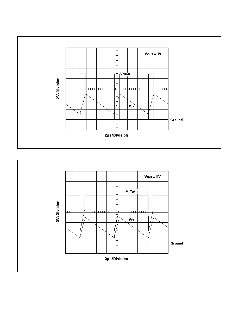
TYPICAL WAVEFORMS
5
UNITRODE INTEGRATED CIRCUITS
7 CONTINENTAL BLVD.
∑
MERRIMACK, NH 03054
TEL. 603-424-2410
∑
FAX 603-424-3460
UCC1889
UCC2889
UCC3889
6

IMPORTANT NOTICE
Texas Instruments and its subsidiaries (TI) reserve the right to make changes to their products or to discontinue
any product or service without notice, and advise customers to obtain the latest version of relevant information
to verify, before placing orders, that information being relied on is current and complete. All products are sold
subject to the terms and conditions of sale supplied at the time of order acknowledgement, including those
pertaining to warranty, patent infringement, and limitation of liability.
TI warrants performance of its semiconductor products to the specifications applicable at the time of sale in
accordance with TI's standard warranty. Testing and other quality control techniques are utilized to the extent
TI deems necessary to support this warranty. Specific testing of all parameters of each device is not necessarily
performed, except those mandated by government requirements.
CERTAIN APPLICATIONS USING SEMICONDUCTOR PRODUCTS MAY INVOLVE POTENTIAL RISKS OF
DEATH, PERSONAL INJURY, OR SEVERE PROPERTY OR ENVIRONMENTAL DAMAGE ("CRITICAL
APPLICATIONS"). TI SEMICONDUCTOR PRODUCTS ARE NOT DESIGNED, AUTHORIZED, OR
WARRANTED TO BE SUITABLE FOR USE IN LIFE-SUPPORT DEVICES OR SYSTEMS OR OTHER
CRITICAL APPLICATIONS. INCLUSION OF TI PRODUCTS IN SUCH APPLICATIONS IS UNDERSTOOD TO
BE FULLY AT THE CUSTOMER'S RISK.
In order to minimize risks associated with the customer's applications, adequate design and operating
safeguards must be provided by the customer to minimize inherent or procedural hazards.
TI assumes no liability for applications assistance or customer product design. TI does not warrant or represent
that any license, either express or implied, is granted under any patent right, copyright, mask work right, or other
intellectual property right of TI covering or relating to any combination, machine, or process in which such
semiconductor products or services might be or are used. TI's publication of information regarding any third
party's products or services does not constitute TI's approval, warranty or endorsement thereof.
Copyright
©
1999, Texas Instruments Incorporated