Document Outline
- FEATURES
- DESCRIPTION
- APPLICATIONS
- ABSOLUTE MAXIMUM RATINGS
- RECOMMENDED OPERATING CONDITIONS
- ORDERING INFORMATION
- PIN ASSIGNMENTS
- ELECTRICAL CHARACTERISTICS
- FUNCTIONAL BLOCK DIAGRAM
- TERMINAL FUNCTIONS
- DETAILED PIN DESCRIPTIONS
- RDEL (pin 1)
- RTON (pin 2)
- RTOFF (pin3)
- VREF (pin 4)
- SYNC (pin 5)
- GND (pin 6)
- CS (pin 7)
- RSLOPE (pin 8)
- FB (pin 9)
- SS/SD (pin 10)
- PGND (pin 11)
- AUX (pin 12)
- OUT (pin 13)
- VDD (pin 14)
- LINEUV (pin 15)
- VIN (pin 16 - UCC2891 and UCC2893 only)
- LINEOV (pin 16 - UCC2892 and UCC2894 only)
- FUNCTIONAL DESCRIPTION
- JFET Control and UVLO
- Line Undervoltage Protection
- Line Overvoltage Protection
- Pulse Skipping
- Synchronization
- APPLICATION INFORMATION: SETUP GUIDE
- Step 1. Oscillator
- Step 2. Soft Start
- Step 3. VDD Bypass Requirements
- Step 4. Delay Programming
- Step 5. Input Voltage Monitoring
- Step 6. Current Sense and Slope Compensation
- ADDITIONAL APPLICATION INFORMATION
- Gate Drive Implementations
- Bootstrap Biasing
- References and Additional Development Tools
- Reference Circuit
- TYPICAL CHARACTERISTICS
- MECHANICAL DRAWINGS
- D (R-PDSO-G**) PLASTIC SMALL-OUTLINE PACKAGE
- PW (R-PDSO-G**) PLASTIC SMALL-OUTLINE PACKAGE
- IMPORTANT NOTICE
UCC2891, UCC2892
UCC2893, UCC2894
SLUS542 - OCTOBER 2003
CURRENT MODE
ACTIVE CLAMP PWM CONTROLLER
1
www.ti.com
FEATURES
D
Ideal for Active Clamp/Reset Forward,
Flyback and Synchronous Rectifier Apps
D
Provides Complementary Auxiliary Driver
with Programmable Deadtime (Turn-On
Delay) between AUX and MAIN Switches
D
Peak Current-Mode Control with
Cycle-by-Cycle Current Limiting
D
TrueDrive
t
2-A Sink, 2-A Source Outputs
D
110-V Input Startup Device on UCC2891/3
D
Trimmed Internal Bandgap Reference for
Accurate Line UV and Line OV Threshold
D
Programmable Slope Compensation
D
High-Performance 1.0-MHz Synchronizable
Oscillator with Internal Timing Capacitor
D
Precise Programmable Maximum Duty Cycle
Limit
APPLICATIONS
D
High-Efficiency Off-Line or DC/DC
Switch-Mode Power Supplies
D
Server Power, 48-V Telecom, Datacom, and
42-V Automotive Applications
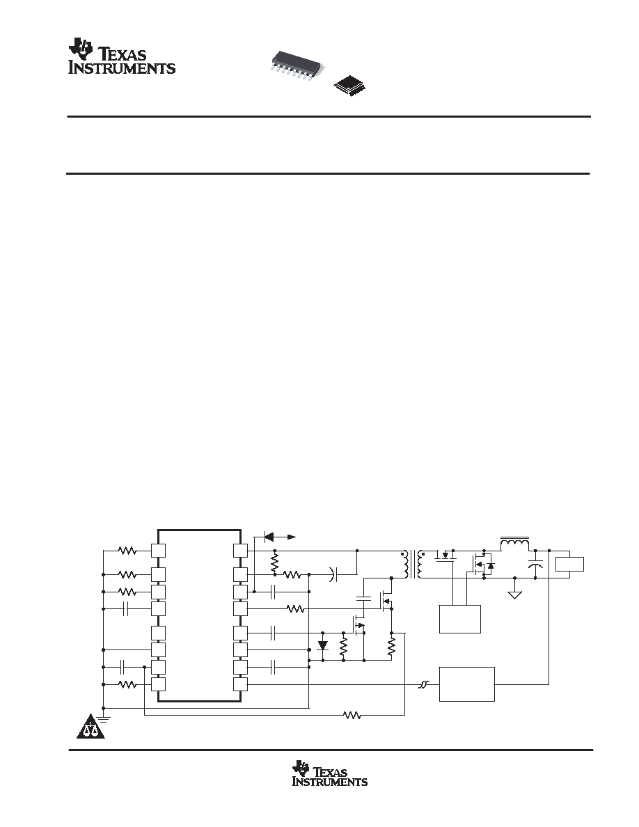
DESCRIPTION
The UCC2891/2/3/4 family of PWM controllers is
designed to simplify implementation of the various
active clamp/reset and synchronous rectifier
switching power topologies.
The UCC289x is a peak current-mode, fixed-
frequency, high-performance pulse width modulator.
It includes the logic and the drive capability for the
auxiliary switch along with a simple method of
programming the critical delays for proper active
clamp operation.
Additional features include an internal
programmable slope compensation circuit,
precise D
MAX
limit, and a synchronizable
oscillator with an internal timing capacitor. An
accurate line monitoring function also programs
the converter's ON and OFF transitions with
regard to the bulk input voltage. These features
allow the power supply designer to eliminate many
of the external components, reducing the size and
complexity of the design.
The devices are offered in 16-pin SOIC (D). The
UCC2892 and UCC2894 is also offered in 16-pin
TSSOP (PW) packages.
CBULK
RCS
UDG-02162
CCLAMP
RF
5
13
12
16
15
1
2
3
RDEL
RTON
RTOFF
SYNC
LINE UV
OUT
AUX
PGND
4
VREF
11
VIN
UCC2891
6
GND
7
CS
8
RSLOPE
14
VDD
SS/SD
10
FB
9
SECONDARY
SIDE E/A
Q1
Q2
LOAD
SR
DRIVE
BIAS
WINDING
+VIN
PRODUCTION DATA information is current as of publication date.
Products conform to specifications per the terms of Texas Instruments
standard warranty. Production processing does not necessarily include
testing of all parameters.
Copyright
2003, Texas Instruments Incorporated
Please be aware that an important notice concerning availability, standard warranty, and use in critical applications of
Texas Instruments semiconductor products and disclaimers thereto appears at the end of this data sheet.

UCC2891, UCC2892
UCC2893, UCC2894
SLUS542 - OCTOBER 2003
2
www.ti.com
These devices have limited built-in ESD protection. The leads should be shorted together or the device placed in conductive foam
during storage or handling to prevent electrostatic damage to the MOS gates.
ABSOLUTE MAXIMUM RATINGS
over operating free-air temperature range unless otherwise noted(1)
UNIT
Supply voltage range, VDD
(IDD < 10 mA)
15
V
Analog inputs
FB, CS
-0.3 to (VREF + 0.3)
not to exceed 6
V
Output source current (peak), IO_SOURCE
OUT, AUX
2.5
A
Output sink current (peak), IO_SINK
OUT, AUX
-2.5
A
Operating junction temperature range, TJ
-55 to 150
Storage temperature, Tstg
-65 to 150
�
C
Lead temperature, Tsol, 1,6 mm (1/16 inch) from case for 10 seconds
300
C
(1) Stresses beyond those listed under "absolute maximum ratings" may cause permanent damage to the device. These are stress ratings only,
and functional operation of the device at these or any other conditions beyond those indicated under "recommended operating conditions" is
not implied. Exposure to absolute-maximum-rated conditions for extended periods may affect device reliability. All voltages are with respect to
GND. Currents are positive into and negative out of, the specified terminal.
RECOMMENDED OPERATING CONDITIONS
MIN
NOM
MAX
UNIT
Supply voltage, VDD
8.5
12.0
14.5
V
Supply bypass capacitance
1
�
F
Timing resistance, RT (for 250-kHz operation)
75
k
Operating junction temperature, TJ
-40
105
�
C
Reference bybass capacitance, CREF
0.1
105
�
F
ORDERING INFORMATION
PART NUMBERS
TA
APPLICATION
AUX
OUTPUT
POLARITY
CS
THRESHOLD
110-V HV JFET
START-UP
CIRCUIT
SOIC-16
(D)
TSSOP-16
(PW)
DC/DC
P-Channel
0.75 V
Yes
UCC2891D
-
-40
�
C to 105
�
C
Off-Line
P-Channel
1.27 V
No
UCC2892D
UCC2892PW
-40
�
C to 105
�
C
DC/DC
N-Channel
0.75 V
Yes
UCC2893D
-
Off-Line
N-Channel
1.27 V
No
UCC2894D
UCC2894PW
The D and PW packages are available taped and reeled. Add R suffix to device type (e.g. UCC2891DR) to order quantities of 2,500
devices per reel (for the D package) and 2,000 devices per reel (for the PW package). Bulk quantities are 40 units per tube (for the D
package) and 90 units per tube (for the PW package).
UCC2891, UCC2892
UCC2893, UCC2894
SLUS542 - OCTOBER 2003
3
www.ti.com
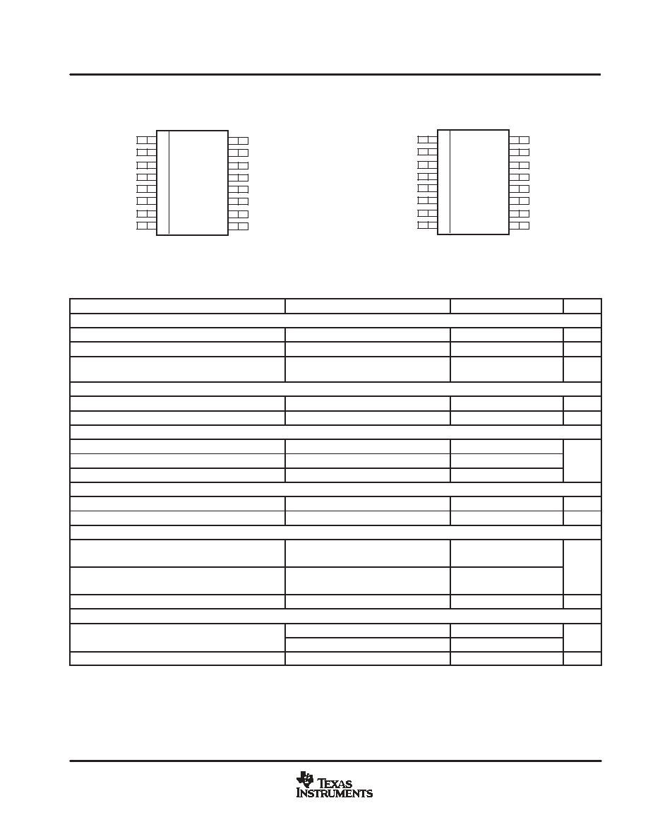
PIN ASSIGNMENTS
RTDEL
RTON
RTOFF
VREF
SYNC
GND
CS
RSLOPE
LINEOV
LINEUV
VDD
OUT
AUX
PGND
SS/SD
FB
1
2
3
4
5
6
7
8
16
15
14
13
12
11
10
9
UCC2892 AND UCC2894
D AND PW PACKAGE
(TOP VIEW)
RTDEL
RTON
RTOFF
VREF
SYNC
GND
CS
RSLOPE
VIN
LINEUV
VDD
OUT
AUX
PGND
SS/SD
FB
1
2
3
4
5
6
7
8
16
15
14
13
12
11
10
9
UCC2891 AND UCC2893
D PACKAGE
(TOP VIEW)
ELECTRICAL CHARACTERISTICS
VDD = 12 V(1), 1-
�
F capacitor from VDD to GND, 0.01-
�
F capacitor from VREF to GND, RT(on) = RT(off) = 75 k
, RDEL = 10 k
,
RSLOPE = 50 k
, -40
�
C
TA = TJ
105
�
C (unless otherwise noted)
PARAMETER
TEST CONDITIONS
MIN
TYP
MAX
UNIT
OVERALL
VDD
Supply voltage range
14.5
V
ISTARTUP Start-up current
VDD < VUVLO start threshold - 0.3V
300
500
�
A
IDD
Operating supply current(1)(2)
VFB = 0 V,
VCS = 0 V,
Outputs not switching
2
3
mA
HIGH-VOLTAGE BIAS SECTION (UCC2891, UCC2893)
V_HV line voltage
80
V
Current rating(3)
10
mA
UNDERVOLTAGE LOCKOUT
Start threshold voltage(1)
12.5
13.0
13.5
Minimum operating voltage after start
7.5
8.0
8.5
V
Hysteresis
4.5
5.0
5.5
V
LINE MONITOR
VLINEUV Line-on voltage(3)
1.243
1.268
1.293
V
ILINEHYS Line hysteresis
11.8
12.5
13.2
�
A
SOFT-START
ISS_CH
Charge current
VRT(on) = 2.5 V / RT(on)
IRTON
-30%
IRTON
IRTON
+30%
mA
ISS_DSH Discharge current
VRT(on) = 2.5 V / RT(on)
IRTON
-30%
IRTON
IRTON
+30%
mA
VSS/SD
Discharge/shutdown threshold voltage
0.4
0.5
0.6
V
VOLTAGE REFERENCE
VREF
Reference voltage
TJ = 25
�
C
4.85
5.00
5.15
V
VREF
Reference voltage
0 A < IREF < 5 mA, over temperature
4.75
5.00
5.25
V
ISC
Short circuit current
REF = 0 V,
TJ = 25
�
C
-20
-11
mA
(1) Set VDD above the start threshold before setting at 12 V.
(2) Does not include current of the external oscillator network.
(3) Ensured by design. Not production tested.

UCC2891, UCC2892
UCC2893, UCC2894
SLUS542 - OCTOBER 2003
4
www.ti.com
ELECTRICAL CHARACTERISTICS
VDD = 12 V(1), 1-
�
F capacitor from VDD to GND, 0.01-
�
F capacitor from VREF to GND, RT(on) = RT(off) = 75 k
, RDEL = 10 k
,
RSLOPE = 50 k
, -40
�
C
TA = TJ
105
�
C (unless otherwise noted)
PARAMETER
TEST CONDITIONS
MIN
TYP
MAX
UNIT
INTERNAL SLOPE COMPENSATION
m
Slope(3)
FB = High
-10%
R
CS
R
SLOPE
+10%
OSCILLATOR
fOSC
Oscillator frequency
TJ = 25
�
C
237
250
263
kHz
Total variation(3)
Line, Temperature
225
270
kHz
VP_P
Oscillator amplitude (peak-to-peak)(3)
2
V
SYNCHRONIZATION
VSYNCH
SYNC theshold voltage
2.3
V
tDEL
SYNC-to-output delay
50
ns
PWM LATCH
Maximum duty cycle
67%
70%
73%
Minimum duty cycle
0%
PWM latch offset
0.5
V
OUTPUT (OUT AND AUX)
tR
Rise time
CLOAD = 2 nF
10
19
28
tF
Fall time
CLOAD = 2 nF
5
14
23
ns
tDEL
Delay time (AUX to OUT)(3)
CLOAD = 2 nF,
RDEL = 10 k
130
160
190
ns
tDEL
Delay time (OUT to AUX)(3)
CLOAD = 2 nF,
RDEL = 10 k
180
IOUT(src)
Output source current(3)
-2
A
IOUT(sink) Output sink current(3)
2
A
VOUT(low) Low-level output voltage
IOUT = 150 mA
0.4
V
VOUT(high) High-level output voltage
IOUT = -150 mA
0.9
V
(1) Set VDD above the start threshold before setting at 12 V.
(2) Does not include current of the external oscillator network.
(3) Ensured by design. Not production tested.
CT
UDG-03147
DMAX
OUT
AUX
(N-channel)
tDEL
tDEL
Figure 1. Output Timing Diagram
UCC2891, UCC2892
UCC2893, UCC2894
SLUS542 - OCTOBER 2003
5
www.ti.com
ELECTRICAL CHARACTERISTICS
VDD = 12 V(1), 1-
�
F capacitor from VDD to GND, 0.01-
�
F capacitor from VREF to GND, RT(on) = RT(off) = 75 k
, RDEL = 10 k
,
RSLOPE = 50 k
, -40
�
C
TA = TJ
105
�
C (unless otherwise noted)
PARAMETER
TEST CONDITIONS
MIN
TYP
MAX
UNIT
CURRENT SENSE
VLVL
Current sense level shift voltage
0.45
0.50
0.55
VERR(max) Maximum voltage error (clamped)(3)
4.8
5.0
5.2
VCS
Current sense threshold
UCC2891
UCC2893
0.71
0.75
0.79
V
VCS
Current sense threshold
UCC2892
UCC2894
1.23
1.27
1.31
(3) Ensured by design. Not production tested.
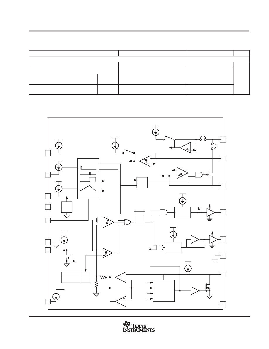
FUNCTIONAL BLOCK DIAGRAM
UDG-03146
I
RDEL
1-D
MAX
D
MAX
V
CT
VIN
(UCC2891/3)
LINEOV
(UCC2892/4)
1
2
3
4
16
15
14
13
LINEUV
VDD
OUT
RDEL
RTON
RTOFF
VREF
5
6
7
8
SYNC
GND
CS
RSLOPE
12
11
10
9
AUX
PGND
SS/SD
FB
2.5 V
2.5 V
2.5 V
SYNC
CLOCK
REF
GEN
VDD
VREF
CT
+
+
S
Q
Q
R
PWM
OFF
VREF
VREF
+
+
0.5 V
OUT
CT
VREF
+
UCC2892/4
UCC2891/3
1.27 V
0.75 V
LINEOV
1.27 V
VREF
+
LINEOV
1.27 V
+
VDD
13 V/ 8 V
OUT
VDD
VDD
UCC2893/UCC2894
UVLO
AND
VDD
VREF
LINEUV
LINEOV
VREF
+
I
SLOPE
I
CHG
I
DSCHG
5
y
I
SLOPE
END
START
3
y
R
2
y
R
0.5
y
I
RDEL
5
y
I
SLOPE
I
RDEL
0.5
y
I
RDEL
0.43
y
I
CHG
Turn-On
Delay
Turn-On
Delay
Enable
N-Channel
1-D
MAX
SOFTSTART

UCC2891, UCC2892
UCC2893, UCC2894
SLUS542 - OCTOBER 2003
6
www.ti.com
TERMINAL FUNCTIONS
TERMINAL
NAME
UCC2891
UCC2893
UCC2892
UCC2894
I/O
DESCRIPTION
AUX
12
12
O
This output drives the auxiliary clamp MOSFET which is turned on when the main PWM
switching device is turned off. The AUX pin can directly drive the auxiliary switch with 2-A
source turn-on current and 2-A sink turn-off current.
CS
7
7
I
This pin is used to sense the peak current utilized for current mode control and for current
limiting functions. The peak signal which can be applied to this pin before pulse-by-pulse
current limiting activates is approximately 0.75 V for the UCC2891 and UCC2893 and 1.27 V
for the UCC2892 and UCC2894.
FB
9
9
I
This pin is used to bring the error signal from an external optocoupler or error amplifier into
the PWM control circuitry. Often, there is a resistor tied from FB to VREF, and an optocoup-
ler is used to pull the control pin closer to GND to reduce the pulse width of the OUT output
driving the main power switch of the converter.
GND
6
6
-
This pin serves as the fundamental analog ground for the PWM control circuitry. This pin
should be connected to PGND directly at the device.
LINEOV
-
16
I
Provides the LINE overvoltage function.
LINEUV
15
15
I
This pin provides a means to accurately enable/disable the power converter stage by moni-
toring the bulk input voltage or another parameter. When the circuit initially starts (or restarts
from a disabled condition), a rising input on LINEUV enables the outputs when the threshold
of 1.27 V is crossed. After the circuit is enabled, then a falling LINEUV signal disables the
outputs when the same threshold is reached. The hysteresis between the two levels is pro-
grammed using an internal current source.
OUT
13
13
O
This output pin drives the main PWM switching element MOSFET in an active clamp control-
ler. It can directly drive an N-channel device with 2-A source turn-on current and 2-A sink
turn-off current.
PGND
11
11
-
The PGND should serve as the current return for the high-current output drivers OUT and
AUX. Ideally, the current path from the outputs to the switching devices, and back would be
as short as possible, and enclose a minimal loop area.
RSLOPE
8
8
I
A resistor connected from this pin to GND programs an internal current source that sets the
slope compensation ramp for the current mode control circuitry.
RTDEL
1
1
I
A resistor from this pin to GND programs the turn-on delay of the two gate drive outputs to
accommodate the resonant transitions of the active clamp power converter.
RTOFF
3
3
I
A resistor connected from this pin to GND programs an internal current source that dis-
charges the internal timing capacitor.
RTON
2
2
I
A resistor connected from this pin to GND programs an internal current source that charges
the internal timing capacitor.
SS/SD
10
10
I
A capacitor from SS/SD to ground is charged by an internal current source of IRTON to pro-
gram the soft-start interval for the controller. During a fault condition this capacitor is dis-
charged by a current source equal to IRTON.
SYNC
5
5
I
The SYNC pin serves as a unidirectional synchronization input for the internal oscillator. The
synchronization function is implemented such that the user programmable maximum duty
cycle (set by RTON and RTOFF) remains accurate during synchronized operation.
VDD
14
14
I
This is the power supply for the device. There should be a 0.1-
�
F capacitor directly from
VDD to PGND.
VIN
16
-
I
For the UCC2891 and UCC2893, this pin is connected to the input power rail directly. Inside
the device, a high-voltage start-up device is utilized to provide the start-up current for the
controller until a bootstrap type bias rail becomes available.
VREF
4
4
O
This is the 5-V reference voltage that can be utilized for an external load of up to 5 mA.
Since this reference provides the supply rail for internal logic, it should be bypassed to
AGND as close as possible to the device.

UCC2891, UCC2892
UCC2893, UCC2894
SLUS542 - OCTOBER 2003
7
www.ti.com
DETAILED PIN DESCRIPTIONS
RDEL (pin 1)
This pin is internally connected to an approximately 2.5-V DC source. A resistor (R
DEL
) to GND (pin 6) sets the
turn-on delay for both gate drive signals of the UCC2981 family of controllers. The delay time is identical for both
switching transitions, between OUT (pin 13) is turning off and AUX (pin 14) is turning on as well as when AUX
(pin 14) is turning off and OUT (pin 13) is turning on. The delay time is defined as:
t
DEL
+
50
10
*
9
)
1.5
10
*
11
R
DEL
For proper selection of the delay time refer to the various references describing the design of active clamp power
converters.
RTON (pin 2)
This pin is internally connected to an approximately 2.5-V DC source. A resistor (R
ON
) to GND (pin 6) sets the
charge current of the internal timing capacitor. The RTON pin, in conjunction with the RTOFF pin (pin 3) are used
to set the operating frequency and maximum operating duty cycle of the UCC2891 family.
RTOFF (pin3)
This pin is internally connected to an approximately 2.5-V DC source. A resistor (R
OFF
) to GND (pin 6) sets the
discharge current of the internal timing capacitor. The RTON and RTOFF pins are used to set the switching
period (T
SW
) and maximum operating duty cycle (D
MAX
) according to the following equations:
t
ON
+
37.33
10
*
12
R
ON
t
OFF
+
16
10
*
12
R
OFF
T
SW
+
t
ON
)
t
OFF
D
MAX
+
t
ON
T
SW
VREF (pin 4)
The controller's internal, 5-V bias rail is connected to this pin. The internal bias regulator requires a good quality
ceramic bypass capacitor (C
VREF
) to GND (pin 6) for noise filtering and to provide compensation to the regulator
circuitry. The recommended C
VREF
value is 0.22-
�
F. The minimum bypass capacitor value is 0.022-
�
F limited
by stability considerations of the bias regulator, while the maximum is approximately 22-
�
F.
The VREF pin is internally current limited and can supply approximately 5-mA to external circuits. The 5-V bias
is only available when the undervoltage lock out (UVLO) circuit enables the operation of UCC289x controllers.
For the detailed functional description of the undervoltage lock out (UVLO) circuit refer to the Functional
Description section of this datasheet.
(1)
(2)
(3)
(4)
(5)

UCC2891, UCC2892
UCC2893, UCC2894
SLUS542 - OCTOBER 2003
8
www.ti.com
DETAILED PIN DESCRIPTIONS (continued)
SYNC (pin 5)
This pin provides an input for an external clock signal which can be used to synchronize the internal oscillator
of the UCC289x family of controllers. The synchronizing frequency must be higher than the free running
frequency of the onboard oscillator T
SYNC
t
T
SW
. The acceptable minimum pulse width of the
synchronization signal is approximately 50 ns (positive logic), and it should remain shorter than
1
*
D
MAX
T
SYNC
where D
MAX
is set by R
ON
and R
OFF
. If the pulse width of the synchronization signal stays
within these limits, the maximum operating duty ratio remains valid as defined by the ratio of R
ON
and R
OFF
,
and D
MAX
is the same in free running and in synchronized modes of operation. If the pulse width of the
synchronization signal would exceed the 1
*
D
MAX
T
SYNC
limit, the maximum operating duty cycle is
defined by the synchronization pulse width.
For more information on synchronization of the UCC2891 family refer to the Functional Description section of
this datasheet.
GND (pin 6)
This pin provides a reference potential for all small signal control and programming circuitry inside the UCC2891
family.
CS (pin 7)
This is a direct input to the PWM and current limit comparators of the UCC2891 family of controllers. The CS
pin should never be connected directly across the current sense resistor (R
CS
) of the power converter. A small,
customary R-C filter between the current sense resistor and the CS pin is necessary to accommodate the
proper operation of the onboard slope compensation circuit and in order to protect the internal discharge
transistor connected to the CS pin (R
F
, C
F
).
Slope compensation is achieved across R
F
by a linearly increasing current flowing out of the CS pin. The slope
compensation current is only present during the on-time of the gate drive signal of the main power switch (OUT)
of the converter. The internal pull-down transistor of the CS pin is activated during the discharge time of the
timing capacitor. This time interval is 1
*
D
MAX
T
SW
long and represents the guaranteed off time of the
main power switch.
RSLOPE (pin 8)
A resistor (R
SLOPE
) connected between this pin and GND (pin 6) sets the amplitude of the slope compensation
current. During the on time of the main gate drive output (OUT) the voltage across R
SLOPE
is a representation
of the internal timing capacitor waveform. As the timing capacitor is being charged, the voltage across R
SLOPE
also increases, generating a linearly increasing current waveform. The current provided at the CS pin for slope
compensation is proportional to this current flowing through R
SLOPE
.
Due to the high speed, AC voltage waveform present at the RSLOPE pin, the parasitic capacitance and
inductance of the external circuit components connected to the RSLOPE pin should be carefully minimized.
For more information on how to program the internal slope compensation refer to the Setup Guide section of
this datasheet.

UCC2891, UCC2892
UCC2893, UCC2894
SLUS542 - OCTOBER 2003
9
www.ti.com
DETAILED PIN DESCRIPTIONS (continued)
FB (pin 9)
This pin is an input for the control voltage of the pulse width modulator of the UCC2891 family. The control
voltage is generated by an external error amplifier by comparing the converters output voltage to a voltage
reference and employing the compensation for the voltage regulation loop. Usually, the error amplifier is located
on the secondary side of the isolated power converter and its output voltage is sent across the isolation
boundary by an opto coupler. Thus, the FB pin is usually driven by the opto coupler. An external pull-up resistor
to the VREF pin (pin 4) is also needed for proper operation as part of the feedback circuitry.
The control voltage is internally buffered and connected to the PWM comparator through a voltage divider to
make it compatible to the signal level of the current sense circuit. The useful voltage range of the FB pin is
between approximately 1.25 V and 4.5 V. Control voltages below the 1.25-V threshold result in zero duty cycle
(pulse skipping) while voltages above 4.5 V result in full duty cycle (D
MAX
) operation.
SS/SD (pin 10)
A capacitor (C
SS
) connected between this pin and GND (pin 6) programs the soft start time of the power
converter. The soft-start capacitor is charged by a precise, internal DC current source which is programmed by
the R
ON
resistor connected to pin 2. The soft-start current is defined as:
I
SS
+
2.5 V
R
ON
0.43
This DC current charges C
SS
from 0 V to approximately 5 V. Internal to the UCC2891 family of controllers, the
soft start capacitor voltage is buffered and ORed with the control voltage present at the FB pin (pin 9). The lower
of the two voltages manipulates the controller's PWM engine through the voltage divider described with regards
to the FB pin. Accordingly, the useful control range on the SS pin is similar to the control range of the FB pin
and it is between 1.25 V and 4.5 V approximately.
PGND (pin 11)
This pin serves as a dedicated connection to all high-current circuits inside the UCC2891 family of parts. The
high-current portion of the controller consists of the two high-current gate drivers, and the various bias
connections except VREF (pin 4). While the PGND (pin 11) and GND (pin 6) pins are connected internally, a
low-impedance, external connection between the two ground pins is also required. It is recommended to form
a separate ground plane for the low current setup components (R
DEL
, R
ON
, R
OFF
, C
VREF
, C
F
, R
SLOPE
, C
SS
and
the emitter of the opto-coupler in the feedback circuit). This separate ground plane (GND) should have a single
connection to the rest of the ground of the power converter (PGND) and this connection should be between pin
6 and pin 11 of the controller.
AUX (pin 12)
This is a high-current gate drive output for the auxiliary switch to implement the active clamp operation for the
power stage. The auxiliary output (AUX) of the UCC2891 and UCC2892 drives a P-channel device as the clamp
switch therefore it requires an active low operation (the switch is ON when the output is low). The UCC2893
and UCC2894 controllers are optimized for N-channel auxiliary switch therefore it employs the traditional active
high drive signal.
(6)

UCC2891, UCC2892
UCC2893, UCC2894
SLUS542 - OCTOBER 2003
10
www.ti.com
DETAILED PIN DESCRIPTIONS (continued)
OUT (pin 13)
This high-current output drives an external N-channel MOSFET. Each controller in the UCC2891 family uses
active high drive signals for the main switch of the converter.
Due to the high speed and high-drive current capability of these outputs (AUX, OUT) the parasitic inductance
of the external circuit components connected to these pins should be carefully minimized. A potential way of
avoiding unnecessary parasitic inductances in the gate drive circuit is to place the controller in close proximity
to the MOSFETs and by ensuring that the outputs (AUX, OUT) and the gates of the MOSFET devices are
connected by wide, overlapping traces.
VDD (pin 14)
The VDD rail is the primary bias for the internal, high-current gate drivers, the internal 5-V bias regulator and
for parts of the undervoltage lockout circuit. To reduce switching noise on the bias rail, a good quality ceramic
capacitor (C
HF
) must be placed very closely between the VDD pin and PGND (pin 11) to provide adequate
filtering. The recommended C
HF
value is 1-
�
F for most applications but its value might be affected by the
properties of the external MOSFET transistors used in the power stage.
In addition to the low-impedance, high-frequency filtering, the controller's bias rail requires a larger value energy
storage capacitor (C
BIAS
) connected parallel to C
HF
. The energy storage capacitor must provide the hold up time
to operate the UCC2891 family (including gate drive power requirements) during start up. In steady state
operation the controller must be powered from a bootstrap winding off the power transformer or by an auxiliary
bias supply. In case of an independent auxiliary bias supply, the energy storage is provided by the output
capacitance of the bias supply.
LINEUV (pin 15)
This input monitors the incoming power source to provide an accurate undervoltage lockout function with user
programmable hysteresis for the power supply controlled by the UCC2891 family. The unique property of the
UCC2891 family is to use only one pin to implement these functions without sacrificing on performance. The
input voltage of the power supply is scaled to the precise 1.27-V threshold of the undervoltage lockout
comparator by an external resistor divider (R
IN1
, R
IN2
). Once the line monitor's input threshold is exceeded, an
internal current source gets connected to the LINEUV pin. The current generator is programmed by the R
DEL
resistor connected to pin 1 of the controller. The actual current level is given as:
I
HYST
+
2.5 V
R
DEL
0.05
As this current flows through R
IN2
of the input divider, the undervoltage lockout hysteresis is a function of I
HYST
and R
IN2
allowing accurate programming of the hysteresis of the line monitoring circuit.
For more information on how to program the line monitoring function refer to the Setup Guide of this datasheet.
(7)

UCC2891, UCC2892
UCC2893, UCC2894
SLUS542 - OCTOBER 2003
11
www.ti.com
DETAILED PIN DESCRIPTIONS (continued)
VIN (pin 16 - UCC2891 and UCC2893 only)
The UCC2891 and UCC2893 controllers are equipped with a high voltage, P-channel JFET start up device to
initiate operation from the input power source of the converter in applications where the input voltage does not
exceed the 110-V maximum rating of the start up transistor. In these applications, the VIN pin can be connected
directly to the positive terminal of the input power source. The internal JFET start up transistor provides
approximately 15-mA charge current for the energy storage capacitor (C
BIAS
) connected across the VDD (pin
14) and PGND (pin 11) terminals. Note that the start up device is turned off immediately when the voltage on
the VDD pin exceeds approximately 13.5 V, the controller's undervoltage lockout threshold for turn-on. The
JFET is also disabled at all times when the high-current gate drivers are switching to protect against excessive
power dissipation and current through the device.
For more information on biasing the UCC2891 family, refer to the Setup Guide and Additional Application
Sections of this datasheet.
LINEOV (pin 16 - UCC2892 and UCC2894 only)
In the UCC2892 and UCC2894 controllers the high-voltage start-up device is not utilized thus pin 16 is used
for a different function. This input monitors the incoming power source to provide an accurate overvoltage
protection with user programmable hysteresis for the power supply controlled by the controller. The circuit
implementation of the overvoltage protection function is identical to the technique used for monitoring the input
power rail for undervoltage lockout. This allows implementing an accurate threshold and hysteresis using only
one pin. The input voltage of the power supply is scaled to the precise 1.27-V threshold of the overvoltage
protection comparator by an external resistor divider (R
IN3
, R
IN4
). Once the line monitor's input threshold is
exceeded, an internal current source gets connected to the LINEOV pin. The current generator is programmed
by the R
DEL
resistor connected to pin 1 of the controller. The actual current level is given as:
I
HYST
+
2.5 V
R
DEL
0.05
As this current flows through R
IN4
of the input divider, the overvoltage protection hysteresis is a function of I
HYST
and R
IN4
allowing accurate programming of the hysteresis of the line monitoring circuit.
For more information on how to program the overvoltage protection, refer to the Setup Guide of this datasheet.
(8)

UCC2891, UCC2892
UCC2893, UCC2894
SLUS542 - OCTOBER 2003
12
www.ti.com
FUNCTIONAL DESCRIPTION
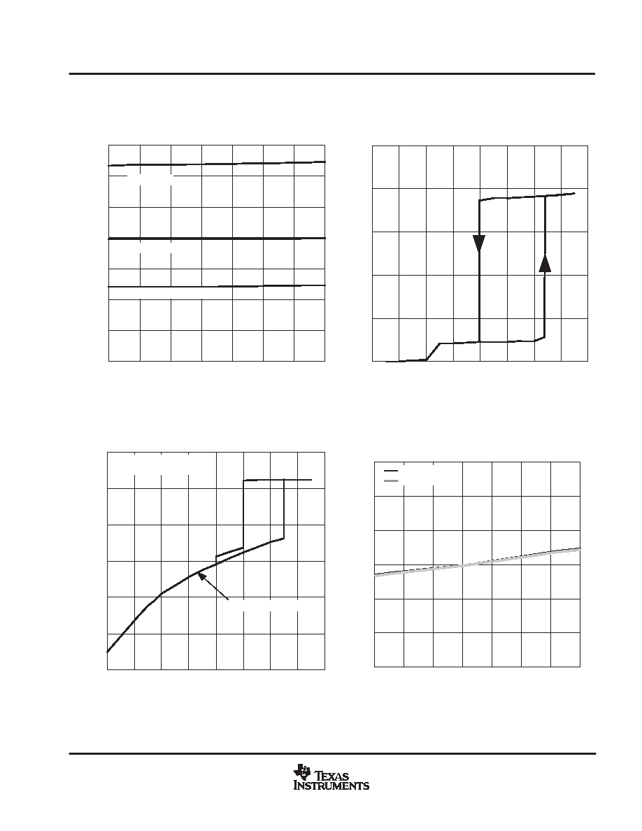
JFET Control and UVLO
The UCC2891 and UCC2893 controllers are outfitted by the high voltage JFET start up transistor. The steady
state power consumption of the of the control circuit which also includes the gate drive power loss of the two
power switches of an active clamp converter exceeds the current and thermal capabilities of the device. Thus
the JFET should only be used for initial start up of the control circuitry and to provide keep-alive power during
stand-by mode when the gate drive outputs are not switching. Accordingly, the start-up device is managed by
its own control algorithm implemented on board the UCC2891 and UCC2893. The following timing diagram
illustrates the operation of the JFET start up device.
VON
VIN
VDD
UDG-03148
OUTPUTs
Bootstrap bias
OFF
SWITCHING
OFF
OFF
SWITCHING
OFF
OFF
OFF
Enable
Command
SS/SD
JFET
Figure 2. JFET Control Startup and Shutdown
During initial power up the JFET is on and charges the C
BIAS
and C
HF
capacitors connected to the VDD pin (pin
14). The VDD pin is monitored by the controller's undervoltage lockout circuit to ensure proper biasing before
the operation is enabled. When the VDD voltage reaches approximately 13.5 V (UVLO turn-on threshold) the
UVLO circuit enables the rest of the controller. At that time, the JFET is turned off and 5 V appears on the VREF
terminal (pin 4). Switching waveforms might not appear at the gate drive outputs unless all other conditions of
proper operation are met. These conditions are:
D
sufficient voltage on the VREF pin (V
VREF
> 4.5V)
D
the voltage on the CS pin is below the current limit threshold
D
the control voltage is above the zero duty cycle boundary (V
FB
> 1.25 V)
D
the input voltage is in the valid operating range (V
VON
<V
VIN
<V
VOFF
) i.e. the line under or overvoltage
protections are not activated.

UCC2891, UCC2892
UCC2893, UCC2894
SLUS542 - OCTOBER 2003
13
www.ti.com
FUNCTIONAL DESCRIPTION
As the controller starts operation it draws its bias power from the C
BIAS
capacitor until the bootstrap winding
takes over. During this time VDD voltage is falling rapidly as the JFET is already off but the bootstrap voltage
is still not sufficient to power the control circuits. It is imperative to store enough energy in C
BIAS
to prevent the
bias voltage to dip below the turn off threshold of the UVLO circuit during the start up time interval. Otherwise
the power supply goes through several cycles of retry attempts before steady state operation might be
established.
During normal operation the bias voltage is determined by the bootstrap bias design. The UCC289x family can
tolerate a wide range of bias voltages between the minimum operating voltage (UVLO turn-off threshold) and
the absolute maximum operating voltage as defined in the datasheet (14 V).
In applications where the power supply must be able to go to stand by in response to an external command,
the bias voltage of the controller must be kept alive to be able to react intelligently to the control signal. In stand
by mode, switching action is suspended for an undefined period of time and the bootstrap power is unavailable
to bias the controller. Without an alternate power source the bias voltage would collapse and the controller would
initiate a re-start sequence. To avoid this situation, the on board JFET of the UCC289x controllers can keep the
VDD bias alive as long as the gate drive outputs remain inactive. As shown in the timing diagram, the JFET is
turned on when VDD = 10 V and charges the C
BIAS
capacitor to approximately 13.5 V. At that time the JFET
turns off and VDD gradually decreases to 10 V then the procedure is repeated. When the power supply is
enabled again, the controller is fully biased and ready to initiate its soft start sequence. As soon as the gate drive
pulses appear the JFET are turned off and bias must be provided by the bootstrap bias generator.
During power down the situation is different as switching action might continue until the VDD bias voltage drops
below the controller's own UVLO turn-off threshold (approximately 8 V). At that time the UCC289x shuts down
completely turning off its 5 V bias rail and returning to start up state when the JFET device is turned on and the
C
BIAS
capacitor starts charging again. In case the converter's input voltage is re-established, the UCC289x
attempts to restart the converter.
Line Undervoltage Protection
When the input power source is removed the power supply is turned off by the line undervoltage protection
because the bootstrap winding keeps the VDD bias up as long as switching takes place in the power stage. As
the power supply's input voltage gradually decreases towards the line cut off voltage the converter's operating
duty cycle must compensate for the lower input voltage. At minimum input voltage the duty cycle nears its
maximum value (D
MAX
). Under these conditions the voltage across the clamp capacitor approaches its highest
value since the transformer must be reset in a relatively short time. The timing diagram in Figure 2 highlights
that in the instance when the converter stops switching the clamp capacitor voltage might be at its maximum
level. Since the clamp capacitor's only load is the power transformer, this high voltage could linger across the
clamp capacitor for a long time when the converter is off. With this high voltage present across the clamp
capacitor a soft start would be very dangerous. Due to the narrow duty cycle of the main switch and the long
on-time of the clamp switch, easily cauing the power transformer to saturate during soft-start.

UCC2891, UCC2892
UCC2893, UCC2894
SLUS542 - OCTOBER 2003
14
www.ti.com
FUNCTIONAL DESCRIPTION
VCLAMP
VIN
VSS
VOFF
TSW
UDG-03149
OUT
AUX
Figure 3. Line Undervoltage Shutdown Waveforms
To eliminate this potential hazard the UCC289x controllers safely discharge the clamp capacitor during power
down. As shown by the timing diagram in Figure 4, the undervoltage lockout circuits stop the power transfer in
the converter by disabling the gate drive signal for the main switch (OUT). The AUX output keeps switching while
the soft-start capacitor C
SS
is being slowly discharged. Notice that the AUX pulse width gradually increases as
the clamp voltage decreases never applying the high voltage across the transformer for extended period of time.
During the slow discharge of the timing capacitor the converter can not be restarted even if the input voltage
returns to the acceptable range.
Line Overvoltage Protection
When the line overvoltage protection is triggered in the UCC2892 and UCC2894 controllers, the gate drive
signals are immediately disabled. At the same time, the slow discharge of C
SS
is initiated. While the soft-start
capacitor is discharging the gate drive signals remains disabled. Once C
SS
= 0.5 V and the overvoltage
disappears from the input of the power supply, operation resumes through a regular soft-start of the converter
as it is demonstrated in Figure 5.

UCC2891, UCC2892
UCC2893, UCC2894
SLUS542 - OCTOBER 2003
15
www.ti.com
FUNCTIONAL DESCRIPTION
OUT
VIN
VSS
VOVP
VOVH
UDG-03150
AUX
Figure 4. Line Overvoltage Sequence
Pulse Skipping
During output load current transients or light load conditions most PWM controllers needs to be able to skip
some number of PWM pulses. In an active clamp topology where the clamp switch is driven complementarily
to the main switch, this would apply the clamp voltage across the transformer continuously. Since operating
conditions might require skipping several switching cycles on the main transistor, saturating the transformer is
very likely if the AUX output stays on.
OUT
AUX
1.25 V
UDG-03151
FB
TSW
D = 0 Boundary
Figure 5. Pulse Skipping Operation
To overcome this problem, the UCC2891 family incorporates pulse skipping for both outputs in the controller.
As can be seen above, when a pulse is skipped at the main output (OUT) because the feedback signal demands
zero duty ratio, the corresponding output pulse on the AUX output is omitted as well. This operation allows to
prevent reverse saturation of the power transformer and to preserve the clamp capacitor voltage level during
pulse skipping operation.

UCC2891, UCC2892
UCC2893, UCC2894
SLUS542 - OCTOBER 2003
16
www.ti.com
FUNCTIONAL DESCRIPTION
Synchronization
The UCC2891 family has a synchronization input pin which can be used to synchronize their oscillator to a
constant frequency system clock. The synchronization signal must have a higher frequency than the free
running oscillator frequency and can be either in-phase or out-of-phase for interleaved operation.
The operation of the oscillator and relevant other waveforms in free running and synchronized mode are shown
in Figure 6.
CT
SYNC
DMAX
OUT
AUX
UDG-03152
Figure 6. Synchronization Waveforms
The most critical and unique feature of the oscillator is to limit the maximum operating duty cycle of the converter.
It is achieved by accurately controlling the charge and discharge intervals of the on board timing capacitor. The
maximum on-time of OUT (pin 13), which is also the maximum duty cycle of the active clamp converter is limited
by the charging interval of the timing capacitor. While the capacitor is being reset to its initial voltage level OUT
is guaranteed to be off.
When synchronization is used, the rising edge of the signal terminates the charging period and initiate the
discharge of the timing capacitor. Once the timing capacitor voltage reaches the predefined valley voltage, a
new charge period starts automatically. This method of synchronization leaves the charge and discharge slopes
of the timing waveform unaffected thus maintains the maximum duty cycle of the converter, independent of the
mode of operation.
Although the synchronization circuit is level sensitive, the actual synchronization event occurs at the rising edge
of the waveform. This allows the synchronizing pulse width to vary significantly but certain limitations must be
observed. The minimum pulse width should be sufficient to guarantee reliable triggering of the internal oscillator
circuitry, therefore it should be greater than approximately 50 nanoseconds. The other limiting factor is to keep
it shorter than 1
*
D
MAX
T
SYNC
where T
SYNC
is the period of the synchronization frequency.

UCC2891, UCC2892
UCC2893, UCC2894
SLUS542 - OCTOBER 2003
17
www.ti.com
FUNCTIONAL DESCRIPTION
When a wider than 1
*
D
MAX
T
SYNC
pulse is connected to the SYNC input, the oscillator is not able to
maintain the maximum duty cycle, originally set by the timing resistor ratio (R
ON
, R
OFF
). Furthermore, the timing
capacitor waveform has a flat portion as highlighted by the vertical marker in the timing diagram. During this
flat portion of the waveform both outputs is off which state is not compatible with the operation of active clamp
power converters. Therefore, this operating mode is not recommended .
Note that both outputs of the UCC289x controllers are off if the synchronization signal stays continuously high.
APPLICATION INFORMATION: SETUP GUIDE
1
2
3
4
16
15
14
13
VIN
LINEUV
VDD
OUT
RDEL
RTON
RTOFF
VREF
UCC2891
UCC2893
5
6
7
8
SYNC
GND
CS
RSLOPE
12
11
10
9
AUX
PGND
SS/SD
FB
POWER ST
AGE
1
2
3
4
16
15
14
13
LINEOV
LINEUV
VDD
OUT
RDEL
RTON
RTOFF
VREF
UCC2892
UCC2894
5
6
7
8
SYNC
GND
CS
RSLOPE
12
11
10
9
AUX
PGND
SS/SD
FB
POWER ST
AGE
RIN1
RDEL
RON
ROFF
CVREF
CF
RSLOPE
CSS
RF
RVREF
CBIAS
CHF
Isolated Feedback
RIN2
+VIN
-VIN
+VIN
-VIN
Isolated Feedback
RIN4
RDEL
RON
ROFF
CVREF
CF
RSLOPE
CSS
RF
RVREF
CBIAS
CHF
RIN2
RIN1
RIN3
Figure 7. UCC289x Typical Setup

UCC2891, UCC2892
UCC2893, UCC2894
SLUS542 - OCTOBER 2003
18
www.ti.com
APPLICATION INFORMATION: SETUP GUIDE
The UCC2891 family offers a highly integrated feature set and excellent accuracy to control an active clamp
forward or active clamp flyback power converter. In order to take advantage of all the benefits integrated in these
controllers, the following procedure can simplify the setup and avoid unnecessary iterations in the design
procedure. Refer to Figure 7 setup diagrams for component names.
Before the controller design begins, the power stage design must be completed. From the power stage design
the following operating parameters are needed to complete the setup procedure of the controller:
D
Switching frequency (f
SW
)
D
Maximum operating duty cycle (D
MAX
)
D
Soft start duration (t
SS
)
D
Gate drive power requirements of the external power MOSFETs (Q
G(main)
, Q
G(aux)
)
D
Bias method and voltage for steady state operation (bootstrap or bias supply)
D
Gate drive turn-on delay (t
DEL
)
D
Turn-on input voltage threshold (V
ON
)
D
Minimum operating input voltage (V
OFF
) where V
IN (off)
< V
IN(on)
D
Maximum operating input voltage (V
OVP
)
D
overvoltage protection hysteresis (V
OVH
)
D
The down slope of the output inductor current waveform reflected across the primary side current sense
resistor dV
L
dt
Step 1. Oscillator
The two timing elements of the oscillator can be calculated from f
SW
and D
MAX
by the following two equations:
R
ON
+
t
ON
37.33
10
*
12
+
D
MAX
f
SW
37.33
10
*
12
R
OFF
+
t
OFF
16
10
*
12
+
1
*
D
MAX
f
SW
16
10
*
12
where D
MAX
is a dimensionless number between 0 and 1.
Step 2. Soft Start
Once R
ON
is defined, the charge current of the soft-start capacitor can be calculated as:
I
SS
+
2.5 V
R
ON
0.43
During soft start, C
SS
is being charged from 0 V to 5 V by the calculated I
SS
current. The actual control range
of the soft-start capacitor voltage is between 1.25 V and 4.5 V. Therefore, the soft-start capacitor value must
be based on this narrower control range and the required start up time (t
SS
) according to:
C
SS
+
I
SS
t
SS
4.5 V
*
1.25 V
(9)
(10)
(11)
(12)

UCC2891, UCC2892
UCC2893, UCC2894
SLUS542 - OCTOBER 2003
19
www.ti.com
APPLICATION INFORMATION: SETUP GUIDE
Note, that t
SS
defines a time interval to reach the maximum current capability of the converter and not the time
required to ramp the output voltage from 0 V to its nominal, regulated level. Using an open-loop start up scheme
does not allow accurate control over the ramp up time of the output voltage. In addition to the I
SS
and C
SS
values,
the time required to reach the nominal output voltage of the converter is a function of the maximum output
current (current limit), the output capacitance of the converter and the actual load conditions. If it is critical to
implement a tightly controlled ramp-up time at the output of the converter, the soft-start must be implemented
using a closed loop technique. Closed loop soft-start can be implemented with the error amplifier of the voltage
regulation loop when its voltage reference is ramped from 0 V to its final steady state value during the required
t
SS
start up time interval.
Step 3. VDD Bypass Requirements
First, the high-frequency filter capacitor is calculated based on the gate charge parameters of the external
MOSFETs. Assuming that the basic switching frequency ripple should be kept below 0.1-V across C
HF
, its value
can be approximated as:
C
HF
+
Q
G(main)
)
Q
G(aux)
0.1 V
The energy storage requirements are defined primarily by the start up time (t
SS
) and turn-on (approximately
13.5 V) and turn-off (approximately 8 V) thresholds of the controller's undervoltage lockout circuit monitoring
the VDD voltage at pin 14. In addition, the bias current consumption of the entire primary side control circuit (I
DD
+ I
EXT
) must be known. This power consumption can be estimated as:
P
BIAS
+
I
DD
)
I
EXT
)
Q
G(main)
)
Q
G(aux)
f
SW
V
DD
During start up (t
SS
) this power is provided by C
BIAS
while its voltage must remain above the UVLO turn-off
threshold. This relationship can be expressed as:
P
BIAS
t
SS
t
1
2
C
BIAS
13.5
2
*
8
2
Rearranging the equation yields the minimum value for C
BIAS
:
C
BIAS
u
2
P
BIAS
t
SS
13.5
2
*
8
2
Step 4. Delay Programming
From the power stage design, the required turn-on delay (t
DEL
) of the gate drive signals is defined. The
corresponding R
DEL
resistor value to implement this delay is given by:
R
DEL
+
t
DEL
*
50
10
*
9
0.87
10
11
(13)
(14)
(15)
(16)
(17)

UCC2891, UCC2892
UCC2893, UCC2894
SLUS542 - OCTOBER 2003
20
www.ti.com
APPLICATION INFORMATION: SETUP GUIDE
Step 5. Input Voltage Monitoring
The input voltage monitoring functions is governed by the following two expressions of the voltage at the
LINEUV terminal (pin 15):
V
VON
+
V
ON
R
IN2
R
IN1
)
R
IN2
at turn on, and
V
VON
+
V
OFF
*
V
VON
R
IN1
)
I
HYST
R
IN2
at turn off.
Since V
ON
and V
OFF
are given by the power supply specification, V
VON
equals the 1.27-V threshold of the line
monitor and I
HYST
is already defined as:
I
HYST
+
2.5 V
R
DEL
0.05
the two unknown, R
IN1
and R
IN2
are fully determined. Solving the equations results the following two
expressions for the input voltage divider:
R
IN1
+
V
ON
*
V
OFF
I
HYST
R
IN2
+
R
IN1
1.27 V
V
ON
*
1.27 V
Similar methods can be used to define the divider components of the overvoltage protection input of the
UCC2892 and UCC2894 controllers.
Step 6. Current Sense and Slope Compensation
The UCC2891 family offers onboard, user programmable slope compensation. The programming of the right
amount of slope compensation is accomplished by the appropriate selection of two external resistors, R
F
and
R
SLOPE
.
First, the current sense filter resistor value (R
F
) must be calculated based on the desired filtering of the current
sense signal. The filter consists of two components, C
F
and R
F
. The C
F
filter capacitor is connected between
the CS pin (pin 7) and the GND terminal (pin 6). While the value of C
F
can be freely selected as the first step
of the filter design, it should be minimized to avoid filtering the slope compensation current exiting the CS pin.
The recommended range for the filter capacitance is between 50 pF and 270 pF. The value of the filter resistor
can be calculated from the filter capacitance and the desired filter corner frequency f
F
.
R
F
+
1
2
p
f
F
C
F
After R
F
is defined R
SLOPE
can be calculated. The amount of slope compensation is defined by the stability
requirements of the inner peak current loop of the control algorithm and is measured by the number m. When
the slope of the applied compensation ramp equals the down slope of the output inductor current waveform
reflected across the primary side current sense resistor dV
L
dt , m equals 1. The minimum value of m is 0.5
to prevent current loop instability. Best current mode performance can be achieved around m=1. The further
increase of m moves the control closer to voltage mode control operation.
(18)
(19)
(20)
(21)
(22)
(23)

UCC2891, UCC2892
UCC2893, UCC2894
SLUS542 - OCTOBER 2003
21
www.ti.com
APPLICATION INFORMATION: SETUP GUIDE
In the UCC289x, controllers slope compensation is implemented by sourcing a linearly increasing current at the
CS pin. When this current passes through the current sense filter resistor (R
F
), it is converted to a slope
compensation ramp which can be characterized by its dV
S
dt . The dV
S
dt of the slope compensation
current is defined by R
SLOPE
according to:
dI
S
dt
+
5
2 V
t
ON
R
SLOPE
where
D
2V is the peak-to-peak ramp amplitude of the internal oscillator waveform
D
5 is the multiplication factor of the internal current mirror
The voltage equivalent of the compensation ramp dV
S
dt can be easily obtained by multiplying with R
F
. After
introducing the application specific m and dV
L
dt values, the equation can be rearranged for R
SLOPE
:
R
SLOPE
+
5
2 V
R
F
t
ON
m
dV
L
dt
(24)
(25)
UCC2891, UCC2892
UCC2893, UCC2894
SLUS542 - OCTOBER 2003
22
www.ti.com
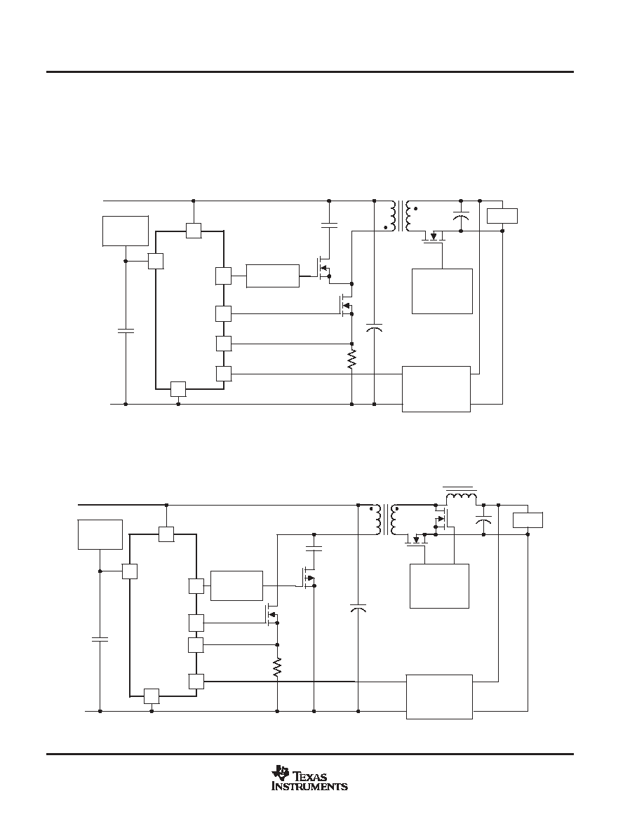
ADDITIONAL APPLICATION INFORMATION
The UCC2891 family of controllers is dedicated to control current mode active clamp flyback or forward
converters in an isolated power supply. The key advantage of the active clamp topologies is the zero voltage
switching (ZVS) of the primary side semiconductors. This operating mode reduces the switching losses of the
converter, thus facilitates higher switching frequencies or improves efficiency when operated at similar
frequencies as its hard switched counterparts. The simplified schematics below demonstrate the typical
implementations of these converters.
UDG-03153
CBIAS
+VIN
-VIN
CCLAMP
QAUX
QMAIN
RCS
9
7
16
14
13
12
FB
VIN
CS
GND
AUX
VDD
OUT
N-Channel
Gate Drive
Secondary-Side
Error Amplifier
and Isolation
Synchronous
Rectifier
Control
6
UCC2893
Bootstrap
Bias
Load
CIN
Figure 8. Zero Voltage Switching Flyback Application
This active clamp flyback converter highlights a high-side clamp circuit using an N-channel MOSFET transistor
as the auxiliary clamp switch.
CBIAS
+VIN
-VIN
CCLAMP
QAUX
QMAIN
RCS
CIN
9
7
14
12
13
FB
VIN
CS
GND
OUT
VDD
AUX
Secondary-Side
Error Amplifier
and Isolation
Synchronous
Rectifier
Control
6
UCC2891
Bootstrap
Bias
Load
P-Channel
Gate Drive
16
UDG-03154
Figure 9. Active Clamp Forward Converter

UCC2891, UCC2892
UCC2893, UCC2894
SLUS542 - OCTOBER 2003
23
www.ti.com
ADDITIONAL APPLICATION INFORMATION
Figure 9 shows an active clamp forward converter with high-side clamp utilizing a P-channel auxiliary switch.
Detailed analysis and design examples of active clamp converters are published in the references listed at the
end of this datasheet.
Gate Drive Implementations
Both topologies can make use of either the high-side or the low-side clamp arrangement. Depending on the
choice of the clamp circuit, the gate drive requirements of the auxiliary switch are different.
CCLAMP
QAUX
QMAIN
+VIN
Figure 10. High-Side N-Channel
12
AUX
P
P
CCLAMP
QAUX
QMAIN
+VIN
Figure 11. Low-Side P-Channel
12
AUX
P
Interfacing with a high side N-channel clamp switch is achievable by using high side gate drive integrated circuits
or through a gate drive transformer. When a transformer is used, special attention must be paid to the fact that
the clamp switch is operated by the complementary waveform of the main power switch. Since the operating
duty cycle of the converter can vary between 0 and D
MAX
, the gate drive transformer must be able to drive the
auxiliary switch with any duty cycle from 1-D
MAX
to near 1.
The low side P-channel gate drive circuit involves a level shifter using a capacitor and a diode which ensures
that the gate drive amplitude of the auxiliary switch is independent of the actual duty cycle of the converter.
Detailed analysis and design examples of these and many similar gate drive solutions are given in reference [6].
Bootstrap Biasing
Many converters use a bootstrap circuit to generate its own bias power during steady state operation. The
popularity of this solutions is justified by the simplicity and high efficiency of the circuit. Usually, bias power is
derived from the main transformer by adding a dedicated, additional winding to the structure. Using a flyback
converter as shown in Figure 12, a bootstrap winding provides a quasi-regulated bias voltage for the primary
side control circuits. The voltage on the VDD pin is equal to the output voltage times the turns ratio between
the output and the bootstrap windings in the transformer. Since the output is regulated, the bias rail is regulated
as well.

UCC2891, UCC2892
UCC2893, UCC2894
SLUS542 - OCTOBER 2003
24
www.ti.com
ADDITIONAL APPLICATION INFORMATION
While the same arrangement can be used in a forward type converter, the bootstrap winding off the main power
transformer would not be able to provide a quasi-regulated voltage. In the forward converter, the voltage across
the bootstrap winding equals the input voltage times the turns ratio. Accordingly the bias voltage would vary with
the input voltage and most likely would exceed the maximum operating voltage of the control circuits at high
line. A linear regulator can be used to limit and regulate the bias voltage if the power dissipation is acceptable.
Another possible solution for the forward converter is to generate the bias voltage from the output inductor as
shown in Figure 13.
16
14
VIN
GND
VDD
Synchronous
Rectifier
Control
6
LOAD
UCC2891
Bootstrap Bias 1
CBIAS
QMAIN
+VIN
CIN
-VIN
UDG-03155
Figure 12. Bootstrap Bias 1, Flyback Example
This solution uses the regulated output voltage across the output inductor during the freewheeling period to
generate a quasi-regulated bias for the control circuits.
UDG-03156
CBIAS
QMAIN
+VIN
CIN
-VIN
16
14
VIN
GND
VDD
Synchronous
Rectifier
Control
6
LOAD
UCC2891
Bootstrap Bias 2
Figure 13. Bootstrap Bias 2, Forward Example

UCC2891, UCC2892
UCC2893, UCC2894
SLUS542 - OCTOBER 2003
25
www.ti.com
ADDITIONAL APPLICATION INFORMATION
This solution uses the regulated output voltage across the output inductor during the freewheeling period to
generate a quasi-regulated bias for the control circuits.
Both of the illustrated solution provides reliable bias power during normal operation. Note that in both cases,
the bias voltages are proportional to the output voltage. This nature of the bootstrap bias supply causes the
converter to operate in a hiccup mode under significant overload or under short-circuit conditions as the
bootstrap winding is not able to hold the bias rail above the undervoltage lockout threshold of the controller.
ADDITIONAL APPLICATION INFORMATION
References and Additional Development Tools
1.
Evaluation Module: UCC2891EVM, 48-V to 3.3-V, 30-A Forward Converter with Active Clamp Reset.
2.
User's Guide: Using the UCC2891EVM, 48-V to 3.3-V, 30-A Forward Converter with Active Clamp Reset,
(SLUU178)
3.
Application Note: Designing for High Efficiency with the UCC2891 Active Clamp PWM Controller, Steve
Mappus (SLUS299)
4.
Power Supply Design Seminar Topic: Design Considerations for Active Clamp and Reset Technique, D.
Dalal, SEM1100-Topic3 (SLUP112)
5.
Power Supply Design Seminar Topic: Active Clamp and Reset Technique Enhances Forward Converter
Performance, B. Andreycak, SEM1000-Topic 3. (SLUP108)
6.
Power Supply Design Seminar Topic: Design and Application Guide for High Speed MOSFET Gate Drive
Circuits, L. Balogh, SEM1400-Topic 2 (SLUP169)
7.
Datasheet: UCC3580, Single Ended Active-Clamp/Reset PWM Controller, (SLUS292A)
8.
Evaluation Module: UCC3580EVM, Flyback Converters, Active Clamp vs. Hard-Switched.
9.
Reference Designs: Highly Efficient 100W Isolated Power Supply Reference Design Using UCC3580-1.
Texas Instruments Hardware Reference Design Number PMP206.
10. Reference Designs: Active Clamp Forward Reference Design using UCC3580-1. Texas Instruments
Hardware Reference Design Number PMP368
Reference Circuit
For completeness, the schematic diagram of a complete active clamp forward converter is shown in Figure 14.
The detailed description of the circuit operation and design procedure can be found in SLUU178.

UCC2891, UCC2892
UCC2893, UCC2894
SLUS542 - OCTOBER 2003
26
www.ti.com
ADDITIONAL APPLICATION INFORMATION
P03001
+
+
+
+
Figure 14. UCC2891 EVM Schematic
UCC2891, UCC2892
UCC2893, UCC2894
SLUS542 - OCTOBER 2003
27
www.ti.com
TYPICAL CHARACTERISTICS
Figure 15
-50
2
0
-25
4
6
8
10
12
14
0
25
50
75
100
125
UVLO VOLTAGE THRESHOLDS
vs
JUNCTION TEMPERATURE
V
UVLO
- UVLO V
oltage
Thresholds - V
TJ - Junction Temperature -
�
C
UVLO On
UVLO Off
UVLO Hysteresis
Figure 16
0
0
2
0.5
1.0
1.5
2.0
2.5
4
6
8
10
12
14
16
QUIESCENT CURRENT
vs
SUPPLY VOLTAGE
I DD
- Supply Current - mA
VDD - Supply Voltage - V
Figure 17
SUPPLY CURRENT
vs
SUPPLY VOLTAGE
0
-50
2
-40
-30
-10
0
10
4
6
8
10
12
14
16
-20
JFET Source Current
UCC2891/UCC2893
VIN = 36 V
I DD
- Supply Current - mA
VDD - Supply Voltage - V
Figure 18
REFERENCE VOLTAGE
vs
TEMPERATURE
V
REF
- Reference V
oltage - V
-50
-40
-30
-10
0
10
-20
-50
-25
0
25
50
75
100
125
TJ - Junction Temperature -
�
C
No Load
10 mA Load
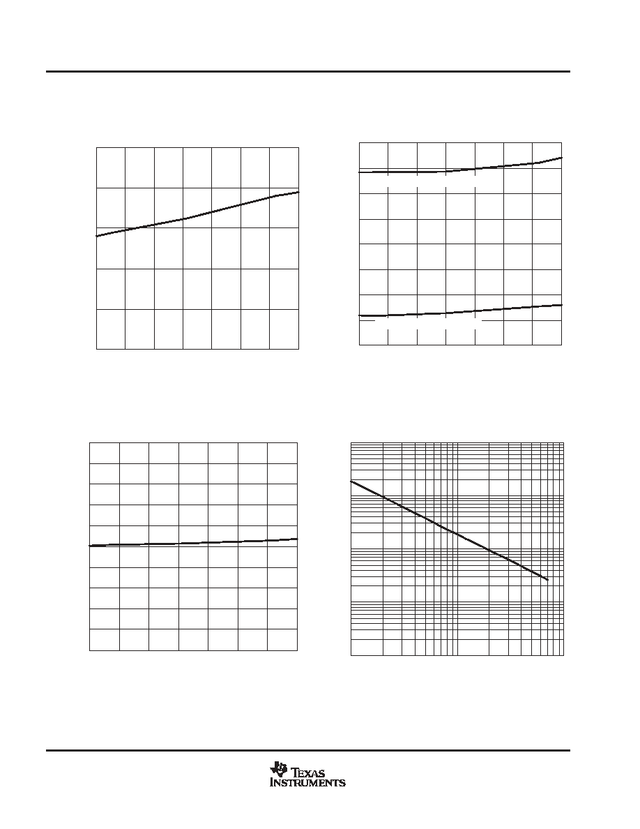
UCC2891, UCC2892
UCC2893, UCC2894
SLUS542 - OCTOBER 2003
28
www.ti.com
TYPICAL CHARACTERISTICS
Figure 19
LINE UV/OV VOLTAGE THRESHOLD
vs
JUNCTION TEMPERATURE
V
TH
- Line Thresholds - V
TJ - Junction Temperature -
�
C
1.20
1.22
1.24
1.26
1.28
1.30
-50
-25
0
25
50
75
100
125
Figure 20
SOFTSTART CURRENTS
vs
TEMPERATURE
I SS(DIS)
/I
SS(CHG)
- Softstart Currents
-
�
A
-50
-25
0
25
50
75
100
125
-20
-15
-10
5
15
20
0
-5
10
TJ - Junction Temperature -
�
C
Softstart Discharge Current
Softstart Charge Current
Figure 21
SOFTSTART/SHUTDOWN THRESHOLD VOLTAGE
vs
JUNCTION TEMPERATURE
V
TH
- Softstart/Shutdown Threshold V
o
ltage - V
-50
0.42
0.40
-25
0
25
50
75
100
125
0.46
0.44
0.50
0.48
0.54
0.52
0.58
0.56
0.60
TJ - Junction Temperature -
�
C
10
1 K
10 K
100 K
10 M
100
1000
1 M
Figure 22
SWITCHING FREQUENCY
vs
PROGRAMMING RESISTANCE
f SW
- Switching Frequency - Hz
RON = ROFF - Timing Resistance - k

UCC2891, UCC2892
UCC2893, UCC2894
SLUS542 - OCTOBER 2003
29
www.ti.com
TYPICAL CHARACTERISTICS
Figure 23
OSCILLATOR FREQUENCY
vs
JUNCTION TEMPERATURE
TJ - Junction Temperature -
�
C
225
230
235
260
270
275
240
-50
-25
0
25
50
75
100
125
245
250
255
265
RON = ROFF = 75 k
f SW
- Switching Frequency - kHz
-50
-25
0
25
50
75
100
125
67
66
69
68
70
72
71
73
74
Figure 24
MAXIMUM DUTY CYCLE
vs
JUNCTION TEMPERATURE
D
MAX
-
Maximum Duty Cycle - %
TJ - Junction Temperature -
�
C
RON = ROFF = 75 k
Figure 25
CURRENT SENSE THRESHOLD VOLTAGE
vs
JUNCTION TEMPERATURE
V
CS
- Current Sense Threshold V
oltage - V
TJ - Junction Temperature -
�
C
0
0.2
0.4
1.0
1.2
1.4
-50
-25
0
25
50
75
100
125
0.6
0.8
UCC2892/UCC2894
UCC2891/UCC2893
Figure 26
SYNCHRONIZATION THRESHOLD VOLTAGE
vs
JUNCTION TEMPERATURE
V
SYNC
- Synchronization Threshold V
o
ltage - V
-50
-25
0
25
50
75
100
125
2.10
2.15
2.20
2.35
2.45
2.50
2.30
2.25
2.40
TJ - Junction Temperature -
�
C

UCC2891, UCC2892
UCC2893, UCC2894
SLUS542 - OCTOBER 2003
30
www.ti.com
TYPICAL CHARACTERISTICS
Figure 27
OUT AND AUX RISE AND FALL TIME
vs
JUNCTION TEMPERATURE
TJ - Junction Temperature -
�
C
t R
/t
F
- Rise and Fall T
imes - ns
-50
5
0
-25
10
15
25
0
25
50
75
100
125
20
Rise Time
Fall Time
CLOAD = 2 nF
Figure 28
DELAY TIME
vs
DELAY RESISTANCE
t DEL
-
Delay T
ime - ns
RDEL - Delay Resistance - k
0
10
20 30 40 50
0
100
500
600
700
200
300
400
-50
0
-25
0
25
50
75
100
125
50
100
150
250
200
Figure 29
DELAY TIME
vs
JUNCTION TEMPERATURE
TJ - Junction Temperature -
�
C
OUT to AUX
AUX to OUT
t DEL
-
Delay T
ime - ns
RDEL = 10 k
-50
0
-25
0
25
50
75
100
125
100
300
500
700
200
800
400
600
Figure 30
TJ - Junction Temperature -
�
C
t DEL
-
Delay T
ime -
�
s
OUT to AUX
AUX to OUT
RDEL = 50 k
DELAY TIME
vs
JUNCTION TEMPERATURE
UCC2891, UCC2892
UCC2893, UCC2894
SLUS542 - OCTOBER 2003
31
www.ti.com
D (R-PDSO-G**)
PLASTIC SMALL-OUTLINE PACKAGE
8 PINS SHOWN
8
0.197
(5,00)
A MAX
A MIN
(4,80)
0.189
0.337
(8,55)
(8,75)
0.344
14
0.386
(9,80)
(10,00)
0.394
16
DIM
PINS **
4040047/E 09/01
0.069 (1,75) MAX
Seating Plane
0.004 (0,10)
0.010 (0,25)
0.010 (0,25)
0.016 (0,40)
0.044 (1,12)
0.244 (6,20)
0.228 (5,80)
0.020 (0,51)
0.014 (0,35)
1
4
8
5
0.150 (3,81)
0.157 (4,00)
0.008 (0,20) NOM
0
�
- 8
�
Gage Plane
A
0.004 (0,10)
0.010 (0,25)
0.050 (1,27)
NOTES: A. All linear dimensions are in inches (millimeters).
B. This drawing is subject to change without notice.
C. Body dimensions do not include mold flash or protrusion, not to exceed 0.006 (0,15).

UCC2891, UCC2892
UCC2893, UCC2894
SLUS542 - OCTOBER 2003
32
www.ti.com
PW (R-PDSO-G**)
PLASTIC SMALL-OUTLINE PACKAGE
14 PINS SHOWN
0,65
M
0,10
0,10
0,25
0,50
0,75
0,15 NOM
Gage Plane
28
9,80
9,60
24
7,90
7,70
20
16
6,60
6,40
4040064/F 01/97
0,30
6,60
6,20
8
0,19
4,30
4,50
7
0,15
14
A
1
1,20 MAX
14
5,10
4,90
8
3,10
2,90
A MAX
A MIN
DIM
PINS **
0,05
4,90
5,10
Seating Plane
0
�
- 8
�
NOTES: D. All linear dimensions are in millimeters.
E. This drawing is subject to change without notice.
F. Body dimensions do not include mold flash or protrusion not to exceed 0,15.

IMPORTANT NOTICE
Texas Instruments Incorporated and its subsidiaries (TI) reserve the right to make corrections, modifications,
enhancements, improvements, and other changes to its products and services at any time and to discontinue
any product or service without notice. Customers should obtain the latest relevant information before placing
orders and should verify that such information is current and complete. All products are sold subject to TI's terms
and conditions of sale supplied at the time of order acknowledgment.
TI warrants performance of its hardware products to the specifications applicable at the time of sale in
accordance with TI's standard warranty. Testing and other quality control techniques are used to the extent TI
deems necessary to support this warranty. Except where mandated by government requirements, testing of all
parameters of each product is not necessarily performed.
TI assumes no liability for applications assistance or customer product design. Customers are responsible for
their products and applications using TI components. To minimize the risks associated with customer products
and applications, customers should provide adequate design and operating safeguards.
TI does not warrant or represent that any license, either express or implied, is granted under any TI patent right,
copyright, mask work right, or other TI intellectual property right relating to any combination, machine, or process
in which TI products or services are used. Information published by TI regarding third-party products or services
does not constitute a license from TI to use such products or services or a warranty or endorsement thereof.
Use of such information may require a license from a third party under the patents or other intellectual property
of the third party, or a license from TI under the patents or other intellectual property of TI.
Reproduction of information in TI data books or data sheets is permissible only if reproduction is without
alteration and is accompanied by all associated warranties, conditions, limitations, and notices. Reproduction
of this information with alteration is an unfair and deceptive business practice. TI is not responsible or liable for
such altered documentation.
Resale of TI products or services with statements different from or beyond the parameters stated by TI for that
product or service voids all express and any implied warranties for the associated TI product or service and
is an unfair and deceptive business practice. TI is not responsible or liable for any such statements.
Following are URLs where you can obtain information on other Texas Instruments products and application
solutions:
Products
Applications
Amplifiers
amplifier.ti.com
Audio
www.ti.com/audio
Data Converters
dataconverter.ti.com
Automotive
www.ti.com/automotive
DSP
dsp.ti.com
Broadband
www.ti.com/broadband
Interface
interface.ti.com
Digital Control
www.ti.com/digitalcontrol
Logic
logic.ti.com
Military
www.ti.com/military
Power Mgmt
power.ti.com
Optical Networking
www.ti.com/opticalnetwork
Microcontrollers
microcontroller.ti.com
Security
www.ti.com/security
Telephony
www.ti.com/telephony
Video & Imaging
www.ti.com/video
Wireless
www.ti.com/wireless
Mailing Address:
Texas Instruments
Post Office Box 655303 Dallas, Texas 75265
Copyright
2003, Texas Instruments Incorporated