 | –≠–ª–µ–∫—Ç—Ä–æ–Ω–Ω—ã–π –∫–æ–º–ø–æ–Ω–µ–Ω—Ç: UCC2895Q | –°–∫–∞—á–∞—Ç—å:  PDF PDF  ZIP ZIP |
UCC1895
UCC2895
UCC3895
DESCRIPTION
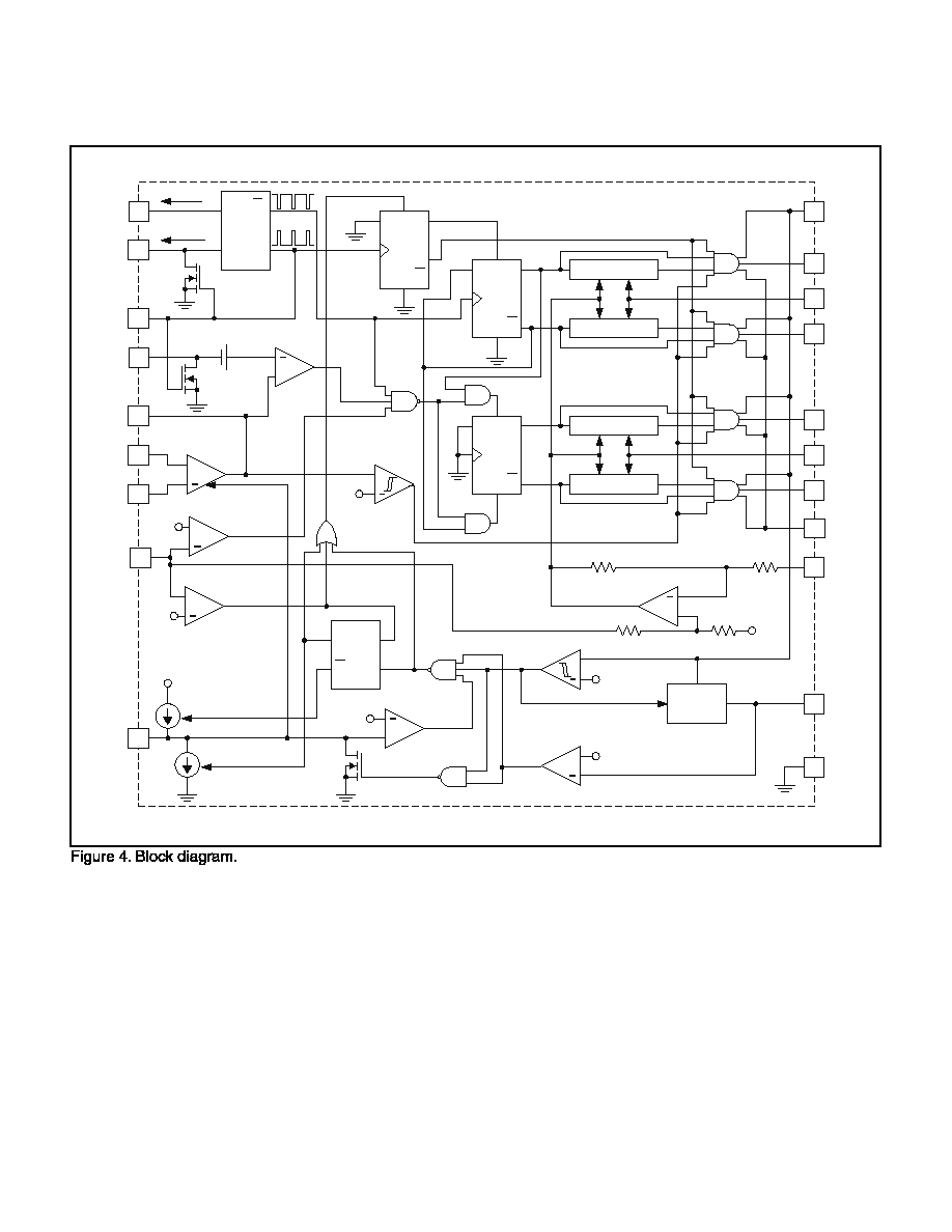
The UCC3895 is a phase shift PWM controller that implements control of a
full-bridge power stage by phase shifting the switching of one half-bridge
with respect to the other. It allows constant frequency pulse-width modula-
tion in conjunction with resonant zero-voltage switching to provide high effi-
ciency at high frequencies. The part can be used either as a voltage mode
or current mode controller.
While the UCC3895 maintains the functionality of the UC3875/6/7/8 family
and UC3879, it improves on that controller family with additional features
such as enhanced control logic, adaptive delay set, and shutdown capabil-
ity. Since it is built in BCDMOS, it operates with dramatically less supply
current than it's bipolar counterparts. The UCC3895 can operate with a
maximum clock frequency of 1MHz.
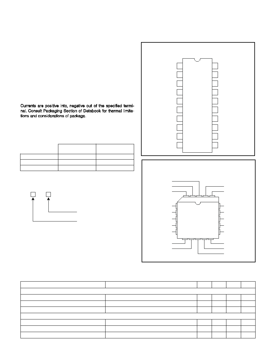
The UCC3895 and UCC2895 are offered in the 20 pin SOIC (DW) pack-
age, 20 pin PDIP (N) package, 20 pin TSSOP (PW) package, and 20 pin
PLCC (Q). The UCC1895 is offered in the 20 pin CDIP (J) package, and 20
pin CLCC package (L).
BiCMOS Advanced Phase Shift PWM Controller
FEATURES
∑
Programmable Output Turn-on Delay
∑
Adaptive Delay Set
∑
Bidirectional Oscillator Synchronization
∑
Capability for Voltage Mode or Current
Mode Control
∑
Programmable Soft Start/Soft Stop
and Chip Disable via a Single Pin
∑
0% to 100% Duty Cycle Control
∑
7MHz Error Amplifier
∑
Operation to 1MHz
∑
Low Active Current Consumption
(5mA Typical @ 500kHz)
∑
Very Low Current Consumption
During Undervoltage Lock-out
(150
m
A typical)
SLUS157B - DECEMBER 1999 - REVISED JANUARY 2001
1
10
11
12
13
14
15
16
17
18
19
7
7
7
7
7
7
7
7
7
20
2
3
4
5
6
7
8
9
UCC3895
EAN
EAP
EAOUT
RAMP
REF
GND
SYNC
CT
RT
DELAB
DELCD
ADS
CS
OUTD
OUTC
VCC
PGND
OUTB
OUTA
SS/DISB
Q1
D
B
A
C
V
IN
V
OUT
V
BIAS
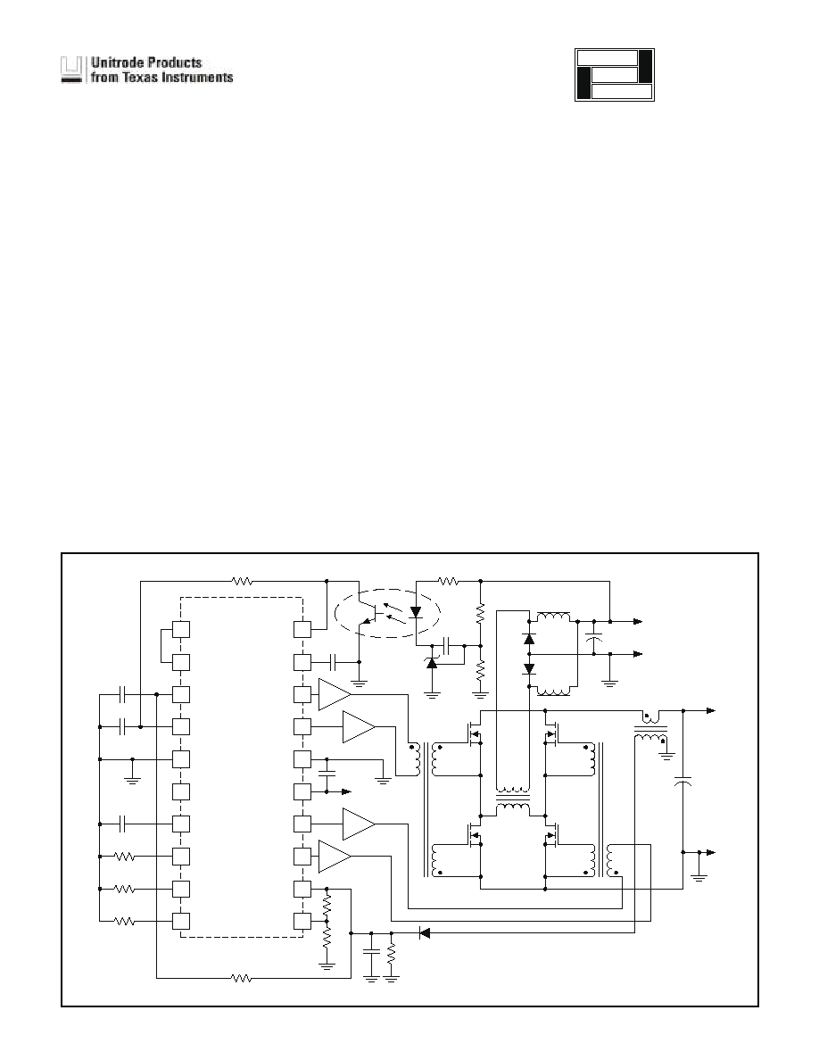
SIMPLIFIED APPLICATION DIAGRAM
UDG-98139
application
INFO
available
2
UCC1895
UCC2895
UCC3895
DIL-20,c SOIC-20, TSSOP-20 (TOP VIEW)
J or N Package, DW Package, PW Package
ABSOLUTE MAXIMUM RATINGS
Supply Voltage (IDD < 10mA) . . . . . . . . . . . . . . . . . . . . . . . 17V
Supply Current . . . . . . . . . . . . . . . . . . . . . . . . . . . . . . . . . 30mA
REF current . . . . . . . . . . . . . . . . . . . . . . . . . . . . . . . . . . . 15mA
OUT Current . . . . . . . . . . . . . . . . . . . . . . . . . . . . . . . . . . 100mA
Analog inputs
(EAP, EAN, EAOUT, RAMP,
SYNC, ADS, CS, SS/DISB) . . . . . . . . . . . ≠0.3V to REF+0.3V
Power Dissipation at T
A
=+25∞C (N Package). . . . . . . . . . . . 1W
Power Dissipation at T
A
=+25∞C (D Package) . . . . . . . . 650mW
Storage Temperature . . . . . . . . . . . . . . . . . . . ≠65∞C to +150∞C
Junction Temperature . . . . . . . . . . . . . . . . . . . ≠55∞C to +125∞C
Lead Temperature (soldering, 10 sec). . . . . . . . . . . . . . +300∞C
OUTA
SS/DISB
EAP
OUTB
PGND
OUTC
VDD
OUTD
EAOUT
EAN
RT
SYNC
CT
RAMP
REF
GND
DELCD
DELAB
CS
20
19
18
17
16
15
14
13
12
11
1
2
3
4
5
6
7
8
9
10
ADS
CONNECTION DIAGRAMS
PLCC-20, CLCC-20 (TOP VIEW)
Q Package, L Package
3
18
17
16
EAN
1
2
20 19
15
14
4
5
6
7
8
9
11
10
12 13
EAOUT
RAMP
EAP
SS/DISB
OUTA
OUTB
OUTC
OUTD
PGND
REF
GND
SYNC
CT
RT
VDD
CS
ADS
DELAB
DELCD
TEMPERATURE
RANGE
PACKAGE
SUFFIX
UCC1895
≠55∞C to +125∞C
J, L
UCC2895
≠40∞C to +85∞C
DW, N, PW, Q
UCC3895
0∞C to +70∞C
DW, N, PW, Q
TEMPERATURE & PACKAGE SELECTION
TABLE
UCC
895
PACKAGE SUFFIX
TEMPERATURE RANGE
ORDERING INFORMATION
ELECTRICAL CHARACTERISTICS:
Unless otherwise specified, VDD=12V, RT=82k
W
, CT=220pF, RDELAB=10k
W
,
RDELCD=10k
W
, C
REF
=0.1
m
F, C
VDD
=1.0
m
F, no load at outputs. T
A
= T
J
. T
A
= 0
∞
C to 70
∞
C for UCC3895x, ≠40
∞
C to +85
∞
C for
UCC2895x, and ≠55
∞
C to +125
∞
C for UCC1895x.
PARAMETER
TEST CONDITIONS
MIN
TYP
MAX
UNITS
UVLO Section
Start Threshold
10.2
11
11.8
V
Stop Threshold
8.2
9
9.8
V
Hysteresis
1.0
2.0
3.0
V
Supply Current
Start-up Current
VDD = 8V
150
250
m
A
I
DD
Active
5
6
mA
VDD Clamp Voltage
IDD = 10mA
16.5
17.5
18.5
V

3
UCC1895
UCC2895
UCC3895
ELECTRICAL CHARACTERISTICS:
Unless otherwise specified, VDD=12V, RT=82k
W
, CT=220pF, RDELAB=10k
W
,
RDELCD=10k
W
, C
REF
=0.1
m
F, C
VDD
=1.0
m
F, no load at outputs. T
A
= T
J
. T
A
= 0
∞
C to 70
∞
C for UCC3895x, ≠40
∞
C to +85
∞
C for
UCC2895x, and ≠55
∞
C to +125
∞
C for UCC1895x.
PARAMETER
TEST CONDITIONS
MIN
TYP
MAX
UNITS
Voltage Reference Section
Output Voltage
T
J
= 25∞C
4.94
5.00
5.06
V
10V < VDD < 17.5V, 0mA < IREF < 5mA,
Temperature
4.85
5
5.15
V
Short Circuit Current
REF = 0V, T
J
= 25∞C
10
20
mA
Error Amplifier Section
Common Mode Input Voltage Range
≠0.1
3.6
V
Offset Voltage
≠7
7
mV
Input Bias Current (EAP, EAN)
≠1
1
m
A
EAOUT VOH
EAP≠EAN = 500mV, I
EAOUT
= ≠0.5mA
4.0
4.5
5.0
V
EAOUT VOL
EAP≠EAN = ≠500mV, I
EAOUT
= 0.5mA
0
0.2
0.4
V
EAOUT Source Current
EAP≠EAN = 500mV, EAOUT= 2.5V
1.0
1.5
mA
EAOUT Sink Current
EAP≠EAN = ≠500mV, EAOUT= 2.5V, (Note 4)
2.5
4.5
mA
Open Loop DC Gain
75
85
dB
Unity Gain Bandwidth
(Note 3)
5.0
7.0
MHz
Slew Rate
EAN from 1V to 0V, EAP = 500mV,
EAOUT from 0.5V to 3.0V, (Note 3)
1.5
2.2
V/
m
s
No Load Comparator Turn-Off Threshold
0.45
0.50
0.55
V
No Load Comparator Turn-On Threshold
0.55
0.60
0.69
V
No Load Comparator Hysteresis
0.035
0.100
0.165
V
Oscillator Section
Frequency
T
J
= 25∞C
473
500
527
kHz
Total Variation
Line, Temperature (Note 3)
2.5
5
%
SYNC VIH
2.05
2.10
2.25
V
SYNC VIL
1.85
1.90
1.95
V
SYNC VOH
I
SYNC
= ≠400
m
A, CT = 2.6V
4.1
4.5
5.0
V
SYNC VOL
I
SYNC
= 100
m
A, CT = 0V
0.0
0.5
1.0
V
SYNC Output Pulse Width
SYNC Load = 3.9k
W
and 30pF in parallel
85
135
ns
RT Voltage
2.9
3
3.1
V
CT Peak Voltage
2.25
2.35
2.50
V
CT Valley Voltage
UCC2895, UCC3895
0.0
0.2
0.4
V
CT Valley Voltage
UCC1895
0.0
0.2
0.6
V
PWM Comparator Section
EAOUT to RAMP Input Offset Voltage
RAMP = 0V, DELAB = DELCD = REF
0.72
0.85
1.05
V
Minimum Phase Shift
(OUTA to OUTC, OUTB to OUTD)
RAMP = 0V, EAOUT = 650mV (Note 1)
0.00
0.85
1.40
%
RAMP to OUTC/OUTD Delay
RAMP from 0V to 2.5V, EAOUT = 1.2V,
DELAB = DELCD = REF (Note 2)
70
120
ns
RAMP Bias Current
RAMP < 5V, CT < 2.2V
≠5
5
m
A
RAMP Sink Current
RAMP = 5V, CT < 2.6V
12
19
mA
Current Sense Section
CS Bias Current
0 < CS , 2.5V, 0 < ADS < 2.5V
≠4.5
20
m
A
Peak Current Threshold
1.90
2.00
2.10
V
Overcurrent Threshold
2.4
2.5
2.6
V
CS to Output Delay
CS from 0 to 2.3V, DELAB = DELCD = REF
75
110
ns

4
UCC1895
UCC2895
UCC3895
ELECTRICAL CHARACTERISTICS:
Unless otherwise specified, VDD=12V, RT=82k
W
, CT=220pF, RDELAB=10k
W
,
RDELCD=10k
W
, C
REF
=0.1
m
F, C
VDD
=1.0
m
F, no load at outputs. T
A
= T
J
. T
A
= 0
∞
C to 70
∞
C for UCC3895x, ≠40
∞
C to +85
∞
C for
UCC2895x, and ≠55
∞
C to +125
∞
C for UCC1895x.
PARAMETER
TEST CONDITIONS
MIN
TYP
MAX
UNITS
Soft Start/Shutdown Section
Soft Start Source Current
SS/DISB = 3.0V, CS < 1.9V
≠40
≠35
≠30
m
A
Soft Start Sink Current
SS/DISB = 3.0V, CS > 2.6V
325
350
375
m
A
Soft Start/Disable Comparator Threshold
0.44
0.50
0.56
V
Delay Set Section
DELAB/DELCD Output Voltage
ADS = CS = 0V
0.45
0.50
0.55
V
ADS = 0V, CS = 2.0V
1.9
2.0
2.1
V
Output Delay
ADS = CS = 0V (Notes 2 and 3)
450
525
600
ns
ADS Bias Current
0V < ADS < 2.5V, 0V < CS < 2.5V
≠20
20
m
A
Output Section
VOH (all outputs)
IOUT = ≠10mA, VDD to Output
250
400
mV
VOL (all outputs)
IOUT = 10mA
150
250
mV
Rise Time
C
LOAD
= 100pF, (Note 3)
20
35
ns
Fall Time
C
LOAD
= 100pF, (Note 3)
20
35
ns
=
∑
-
200
t
t
t
f OUTA
f OUTC
PERIOD
(
)
(
)
=
∑
-
200
t
t
t
f OUTB
f OUTD
PERIOD
(
)
(
)
t
DELAY
= t
f(OUTA)
- t
r(OUTB)
OUTA
OUTB
t
DELAY
= t
f(OUTA)
- t
f(OUTC)
t
PERIOD
OUTA
OUTC

5
UCC1895
UCC2895
UCC3895
PIN DESCRIPTIONS
ADS: Adaptive Delay Set. This function sets the ratio be-
tween the maximum and minimum programmed output
delay dead time. When the ADS pin is directly connected
to the CS pin, no delay modulation occurs. The maximum
delay modulation occurs when ADS is grounded. In this
case, delay time is four times longer when CS = 0 than
when CS = 2.0V (the Peak Current threshold), ADS
changes the output voltage on the delay pins DELAB and
DELCD by the following formula:
(
)
[
]
V
V
V
V
DEL
CS
ADS
=
∑
-
+
0 75
0 5
.
.
where V
CS
and V
ADS
are in Volts. ADS must be limited to
between 0V and 2.5V and must be less than or equal to
CS. DELAB and DELCD also will be clamped to a mini-
mum of 0.5V.
EAOUT: Error Amplifier Output. It is also connected inter-
nally to the non-inverting input of the PWM comparator
and
the
no-load
comparator. EAOUT
is
internally
clamped to the soft start voltage. The no-load comparator
shuts down the output stages when EAOUT falls below
500mV, and allows the outputs to turn-on again when
EAOUT rises above 600mV.
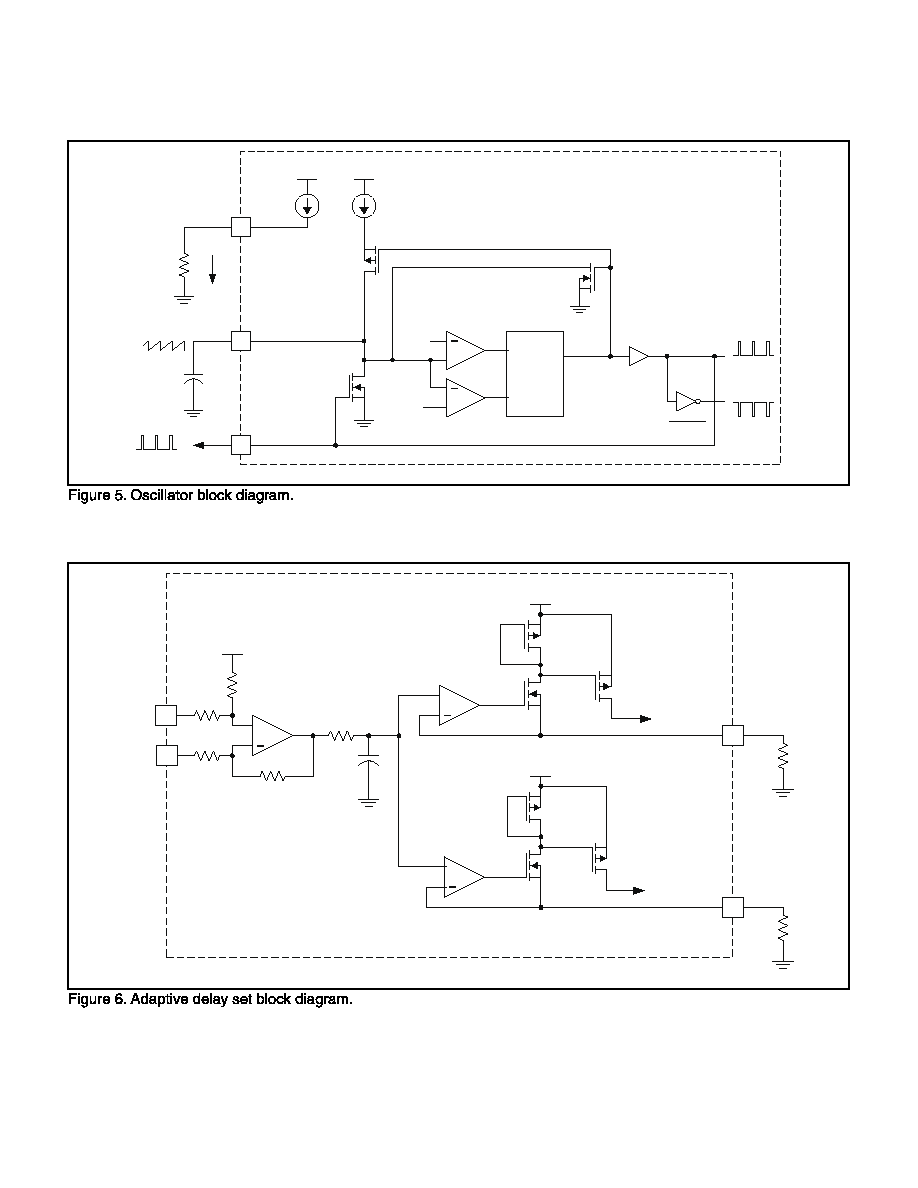
CT: Oscillator Timing Capacitor. (Refer to Fig. 1, Oscilla-
tor Block Diagram) The UCC3895's oscillator charges CT
via a programmed current. The waveform on C
T
is a
sawtooth, with a peak voltage of 2.35V. The approximate
oscillator period is calculated by the following formula:
t
R
C
ns
OSC
T
T
=
∑
∑
+
5
48
120
where C
T
is in Farads, and R
T
is in Ohms and t
OSC
is in
seconds. C
T
can range from 100pF to 880pF. Please
note that a large C
T
and a small R
T
combination will re-
sult in extended fall times on the C
T
waveform. The in-
creased fall time will increase the SYNC pulse width,
hence limiting the maximum phase shift between OUTA,
OUTB and OUTC, OUTD outputs, which limits the maxi-
mum duty cycle of the converter.
CS: Current Sense. This is the inverting input of the Cur-
rent Sense comparator and the non-inverting input of the
Over-current comparator, and the ADS amplifier. The cur-
rent sense signal is used for cycle-by-cycle current limit-
ing in peak current mode control, and for overcurrent
protection in all cases with a secondary threshold for out-
put
shutdown. An
output
disable
initiated
by
an
overcurrent fault also results in a restart cycle, called
"soft stop", with full soft start.
DELAB,
DELCD:
Delay
Programming
Between
Complementary Outputs. DELAB programs the dead
time between switching of OUTA and OUTB, and DELCD
programs the dead time between OUTC and OUTD. This
delay is introduced between complementary outputs in
the same leg of the external bridge. The UCC3895 allows
the user to select the delay, in which the resonant
switching of the external power stages takes place.
Separate delays are provided for the two half-bridges to
accommodate differences in resonant capacitor charging
currents. The delay in each stage is set according to the
following formula:
(
)
t
R
V
ns
DELAY
DEL
DEL
=
∑
∑
+
-
25 10
25
12
where V
DEL
is in Volts, and R
DEL
is in Ohms and t
DELAY
is in seconds.
DELAB and DELCD can source about
1mA maximum. Choose the delay resistors so that this
maximum is not exceeded. Programmable output delay
can be defeated by tying
DELAB
and/or DELCD to REF.
For an optimum performance keep stray capacitance on
these pins at <10pF.
EAP: The non-inverting input to the error amplifier.
EAN: The inverting input to the error amplifier.
GND: Chip ground for all circuits except the output
stages.
OUTA, OUTB, OUTC, OUTD: The 4 outputs are 100mA
complementary MOS drivers, and are optimized to drive
FET
driver
circuits.
OUTA
and
OUTB
are
fully
complementary, (assuming no programmed delay). They
operate near 50% duty cycle and one-half the oscillating
frequency. OUTA and OUTB are intended to drive one
half-bridge circuit in an external power stage. OUTC and
OUTD will drive the other half-bridge and will have the
same characteristics as OUTA and OUTB. OUTC is
phase shifted with respect to OUTA, and OUTD is phase
shifted with respect to OUTB. Note that changing the
phase relationship of OUTC and OUTD with respect to
OUTA and OUTB requires other than the nominal 50%
duty ratio on OUTC and OUTD during those transients.
PGND: Output Stage Ground. To keep output switching
noise from critical analog circuits, the UCC3895 has 2
different ground connections. PGND is the ground
connection for the high-current output stages. Both GND
and PGND must be electrically tied together closely near
the IC. Also, since PGND carries high current, board
traces must be low impedance.

Programming DELAB, DELCD, and the Adaptive Delay Set
The UCC3895 allows the user to set the delay between
switch commands within each leg of the full bridge power
circuit according to the following formula from the data
sheet:
t
R
V
n
DELAY
DEL
DEL
=
∑
∑
+
-
(
)
sec
25 10
25
12
For this equation V
DEL
is determined in conjunction with
the desire to utilize (or not utilize) the adaptive delay set
feature from the following formula:
(
)
[
]
V
V
V
V
DEL
CS
ADS
=
∑
-
+
0 75
0 5
.
.
The following diagram illustrates the resistors needed to
program the delay periods and the adaptive delay set
function.
APPLICATION INFORMATION
6
UCC1895
UCC2895
UCC3895
RAMP: The Inverting Input of the PWM Comparator. This
pin receives either the CT waveform in voltage and aver-
age current mode controls, or the current signal (plus
slope compensation) in peak current mode control. An in-
ternal discharge transistor is provided on RAMP, which is
triggered during the oscillator dead time.
RT: Oscillator Timing Resistor. (Refer to Fig. 1, Oscillator
Block Diagram) The oscillator in the UCC3895 operates
by charging an external timing capacitor, CT, with a fixed
current programmed by R
T.
R
T
current is calculated as
follows:
I
V
R
RT
T
=
3 0
.
where R
T
is in Ohms and I
RT
is in Amperes. R
T
can
range from 40k
W
to 120k
W
Soft start charging and dis-
charging current are also programmed by I
RT
.
SS/DISB: Soft Start/Disable. This pin combines the two
independent functions.
: A rapid shutdown of the chip is
accomplished by any one of the following: externally
forcing SS/DISB below 0.5V, externally forcing REF
below 4V, V
DD
dropping below the UNLO threshold, or an
overcurrent fault is sensed (CS = 2.5V).
In the case of REF being pulled below 4V or an UVLO
condition, SS/DISB is actively pulled to ground via an
internal MOSFET switch. If an overcurrent is sensed,
SS/DISB will sink a current of (10
∑
I
RT
) until SS/DISB
falls below 0.5V.
Note that if SS/DISB is externally forced below 0.5V the
pin will start to source current equal to I
RT
. Also note that
the only time the part switches into the low IDD current
mode is when the part is in undervoltage lockout.
After a fault or disable condition has
passed, VDD is above the start threshold, and/or
SS/DISB falls below 0.5V during a soft stop, SS/DISB will
switch to a soft start mode.
The pin will now source
current, equal to I
RT
.
A user-selected capacitor on
SS/DISB determines the soft start (and soft-start) time. In
addition, a resistor in parallel with the capacitor may be
used, limiting the maximum voltage on SS/DISB. Note
that SS/DISB will actively clamp the EAOUT pin voltage
to approximately the SS/DISB pin voltage during both
soft start, soft stop, and disable conditions.
SYNC: Oscillator Synchronization. (Refer to Fig. 1, Oscil-
lator Block Diagram) This pin is bidirectional. When used
as an output, SYNC can be used as a clock, which is the
same as the chip's internal clock. When used as an in-
put, SYNC will override the chip's internal oscillator and
act as it's clock signal. This bidirectional feature allows
synchronization of multiple power supplies. The SYNC
signal will also internally discharge the CT capacitor and
any filter capacitors that are present on the RAMP pin.
The internal SYNC circuitry is level sensitive, with an in-
put low threshold of 1.9V, and an input high threshold of
2.1V. A resistor as small as 3.9k
W
may be tied between
SYNC and GND to reduce the sync pulse width.
VDD: Power Supply. VDD must be bypassed with a mini-
mum of a 1.0
m
F low ESR, low ESL capacitor to ground.
REF: 5V,
±
1.2% voltage reference. The reference
supplies power to internal circuitry, and can also supply
up to 5mA to external loads. The reference is shut down
during undervoltage lock-out but is operational during all
other disable modes. For best performance, bypass with
a 0.1
m
F low ESR, low ESL capacitor to ground.
PIN DESCRIPTIONS (cont.)
9
11
10
12
DELCD
DELAB
ADS
CS
R
DELCD
R
DELAB
UCC3895

7
UCC1895
UCC2895
UCC3895
The Adaptive Delay Set feature (ADS) allows the user to
vary the delay times between switch commands within
each of the converter's two legs. The delay time modula-
tion is implemented by connecting ADS (pin 11) to CS,
GND, or a resistive divider from CS to GND to set V
ADS
.
From the equation for V
DEL
above, if ADS is tied to GND
then V
DEL
rises in direct proportion to V
CS
, causing a de-
crease in t
DELAY
as the load increases. In this condition
the maximum value of V
DEL
is 2V. If ADS is connected to
a resistive divider between CS and GND the term
(V
CS
-V
DS
) becomes smaller, reducing the level of V
DEL
.
This will decrease the amount of delay modulation. In the
limit of ADS tied to CS, V
DEL
=0.5V and no delay modula-
tion occurs. In the case with maximum delay modulation
(ADS=GND), when the circuit goes from light load to
heavy load the variation of V
DEL
is from 0.5V to 2V. This
causes the delay times to vary by a 4:1 ratio as the load
is changed.
The ability to program an adaptive delay is a desirable
feature because the optimum delay time is a function of
the current flowing in the primary winding of the trans-
former, and can change by a factor of 10:1 or more as
circuit loading changes. Reference [1] delves into the
many interrelated factors for choosing the optimum delay
times for the most efficient power conversion, and illus-
trates an external circuit to enable adaptive delay set us-
ing the UC3879. Implementing this adaptive feature is
simplified in the UCC3895 controller, giving the user the
ability to tailor the delay times to suit a particular applica-
tion with a minimum of external parts.
[1]
L. Balogh,
Unitrode Power
Supply Design Seminar Manual, Unitrode Corporation,
1996, Topic 2.
APPLICATION INFORMATION (CONT.)
CLOCK
RAMP
&
COMP
PWM
SIGNAL
OUTPUT A
OUTPUT B
OUTPUT C
OUTPUT D
UDG-98138
0
0.5
1.0
100
1.5
2.0
2.5
200
300
400
500
A=1.0
A=0.8
A=0.6
A=0.4
A=0.2
A=0.1
CURRENT SENSE VOLTAGE (V)
D
E
L
A
YT
I
M
E(
n
s
)
A = V
ADS
/V
CS
R
DELAY
= 10k
W
8
UCC1895
UCC2895
UCC3895
OSC
Q
Q
Q
Q
D
Q
Q
S
R
0.5V
11 V / 9 V
Q
Q
D
Q
D
2 V
2.5 V
REF
4 V
0.5 V
REF
0.5 V / 0.6 V
19
8
7
6
2
20
1
12
5
4
11
16
13
10
14
17
9
18
15
+
3
SS
CS
EAN
EAP
EAOUT
RAMP
SYNC
CT
RT
GND
REF
ADS
OUTD
PGND
DELCD
OUTC
OUTB
DELAB
OUTA
VDD
DELAY C
DELAY D
DELAY A
DELAY B
Q
HI=ON
I
RT
10(I
RT
)
DISABLE
COMPARATOR
OVER CURRENT
COMPARATOR
ERROR
AMP
CURRENT SENSE
COMPARATOR
PWM
COMPARATOR
S
R
S
R
I
RT
8(I
RT
)
NO LOAD
COMPARATOR
HI=ON
S
R
0.8 V
ADAPTIVE DELAY
SET AMPLIFIER
UVLO COMPARATOR
REFERENCE OK
COMPARATOR
+
+
+
+
+
+
+
+
+
APPLICATION INFORMATION (cont.)
UDG-98140
9
UCC1895
UCC2895
UCC3895
0.5 V
75 k
75 k
100 k
ADS
CS
DELCD
DELAB
REF
TO DELAY A
AND DELAY B
BLOCKS
REF
TO DELAY C
AND DELAY D
BLOCKS
+
+
+
100 k
UDG-98142
SYNC
C
T
S
R
Q
V
REF
CLOCK
CLOCK
0.2 V
2.5 V
REF
RT
I
RT
CT
R
T
8I
RT
+
+
CIRCUIT DESCRIPTION
UDG-98141

10
UCC1895
UCC2895
UCC3895
0
200
400
600
800
1000
1200
1400
1600
100
1000
CT (pF)
FREQ
UENCY
(kHz)
RT=47K
RT=62k
RT=82k
RT=100k
0.8
0.85
0.9
0.95
1
-60
-40
-20
0
20
40
60
80
100
120
TEMPERATURE (∞C)
EA
OUT
T
O
RAMP
O
FFSET
(V)
V
REF
DELAYED
CLOCK
SIGNAL
3.5V
DELAB/CD
FROM PAD
2.5V
CLOCK
BUSSED CURRENT
FROM ADS CIRCUIT
CIRCUIT DESCRIPTION (cont.)
UDG-98143
0
20
40
60
80
100
1
100
10000
1000000
FREQUENCY (Hz)
GAIN
(dB)
0
40
80
120
160
200
PHASE
M
ARGIN
(DEGREES)
GAIN (dB)
PHASE MARGIN (∞C)
0
200
400
600
800
1000
1200
1400
1600
1800
2000
0
10
20
30
40
RDEL (k
W
)
OUTPUT
DELAY
(
ns)
Vcs=0V
Vcs=2V
TYPICAL CHARACTERISTIC
11
UCC1895
UCC2895
UCC3895
4
5
6
7
8
9
10
11
12
13
0
400
800
1200
1600
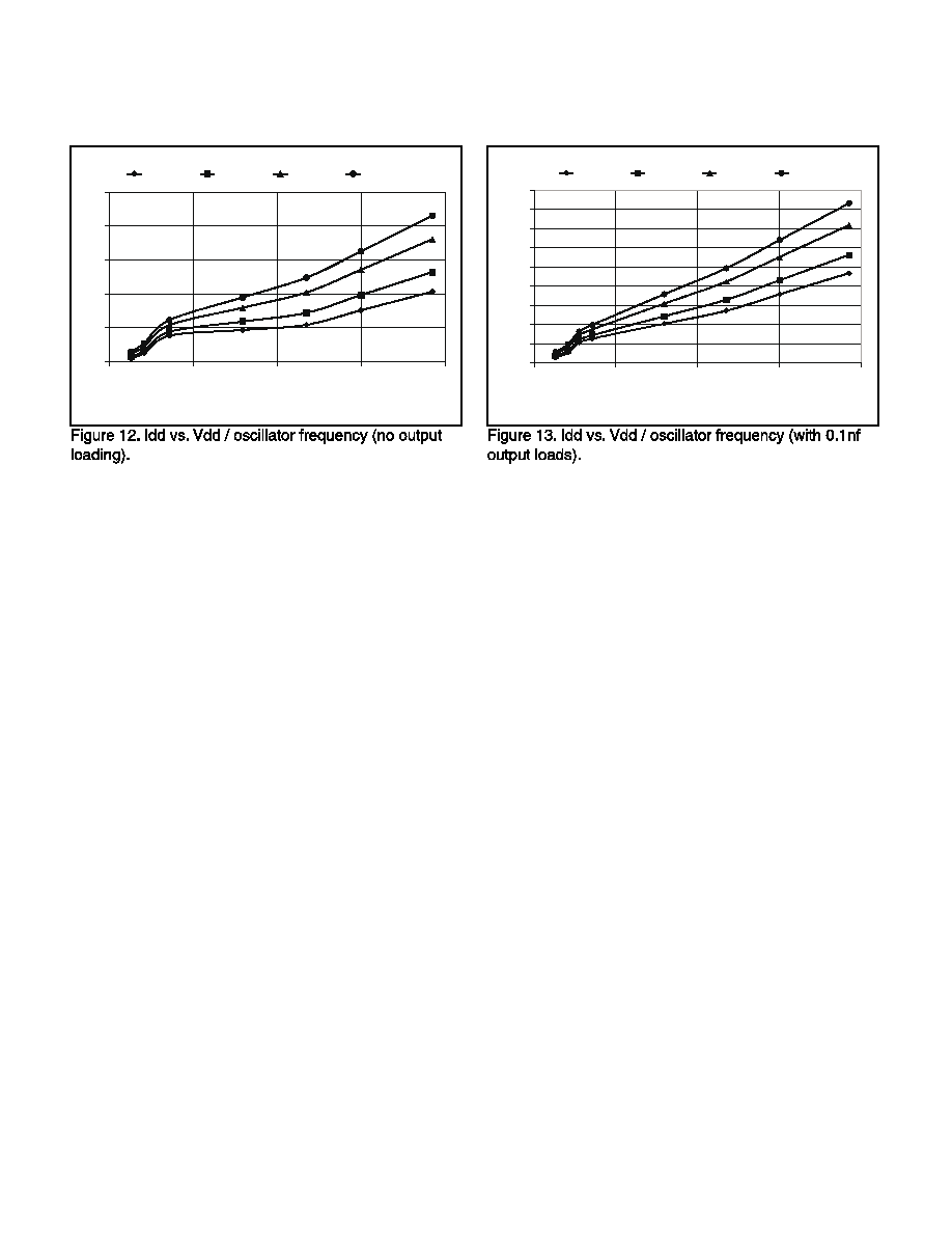
OSCILLATOR FREQUENCY (kHz)
Id
d
(
mA
)
Vdd=10V
Vdd=12V
Vdd=15V
Vdd=17V
4
5
6
7
8
9
0
400
800
1200
1600
OSCILLATOR FREQUENCY (kHz)
Id
d
(
mA)
Vdd=10V
Vdd=12V
Vdd=15V
Vdd=17V
TYPICAL CHARACTERISTIC (cont.)

PACKAGING INFORMATION
Orderable Device
Status
(1)
Package
Type
Package
Drawing
Pins Package
Qty
Eco Plan
(2)
Lead/Ball Finish
MSL Peak Temp
(3)
UCC1895J
ACTIVE
CDIP
J
20
1
None
A42 SNPB
Level-NC-NC-NC
UCC1895L
ACTIVE
LCCC
FK
20
1
None
POST-PLATE
Level-NC-NC-NC
UCC2895DW
ACTIVE
SOIC
DW
20
25
None
CU SNPB
Level-2-220C-1 YEAR
UCC2895DWTR
ACTIVE
SOIC
DW
20
2000
None
CU SNPB
Level-2-220C-1 YEAR
UCC2895N
ACTIVE
PDIP
N
20
20
None
CU SNPB
Level-NA-NA-NA
UCC2895PW
ACTIVE
TSSOP
PW
20
70
None
CU NIPDAU
Level-2-220C-1 YEAR
UCC2895PWTR
ACTIVE
TSSOP
PW
20
2000
None
CU NIPDAU
Level-2-220C-1 YEAR
UCC2895PWTRG4
PREVIEW
TSSOP
PW
20
2000
None
Call TI
Call TI
UCC2895Q
ACTIVE
PLCC
FN
20
46
None
CU SNPB
Level-2-220C-1 YEAR
UCC2895QTR
ACTIVE
PLCC
FN
20
1000
None
CU SNPB
Level-2-220C-1 YEAR
UCC3895DW
ACTIVE
SOIC
DW
20
25
None
CU SNPB
Level-2-220C-1 YEAR
UCC3895DWTR
ACTIVE
SOIC
DW
20
2000
None
CU SNPB
Level-2-220C-1 YEAR
UCC3895DWTRG4
ACTIVE
SOIC
DW
20
2000 Green (RoHS &
no Sb/Br)
CU NIPDAU
Level-1-260C-UNLIM
UCC3895N
ACTIVE
PDIP
N
20
20
None
CU SNPB
Level-NA-NA-NA
UCC3895PW
ACTIVE
TSSOP
PW
20
70
None
CU NIPDAU
Level-2-220C-1 YEAR
UCC3895PWTR
ACTIVE
TSSOP
PW
20
2000
None
CU NIPDAU
Level-2-220C-1 YEAR
UCC3895PWTRG4
ACTIVE
TSSOP
PW
20
2000 Green (RoHS &
no Sb/Br)
CU NIPDAU
Level-2-260C-1 YEAR
UCC3895Q
ACTIVE
PLCC
FN
20
46
None
CU SNPB
Level-2-220C-1 YEAR
UCC3895QTR
ACTIVE
PLCC
FN
20
1000
None
CU SNPB
Level-2-220C-1 YEAR
(1)
The marketing status values are defined as follows:
ACTIVE: Product device recommended for new designs.
LIFEBUY: TI has announced that the device will be discontinued, and a lifetime-buy period is in effect.
NRND: Not recommended for new designs. Device is in production to support existing customers, but TI does not recommend using this part in
a new design.
PREVIEW: Device has been announced but is not in production. Samples may or may not be available.
OBSOLETE: TI has discontinued the production of the device.
(2)
Eco Plan - May not be currently available - please check
http://www.ti.com/productcontent
for the latest availability information and additional
product content details.
None: Not yet available Lead (Pb-Free).
Pb-Free (RoHS): TI's terms "Lead-Free" or "Pb-Free" mean semiconductor products that are compatible with the current RoHS requirements
for all 6 substances, including the requirement that lead not exceed 0.1% by weight in homogeneous materials. Where designed to be soldered
at high temperatures, TI Pb-Free products are suitable for use in specified lead-free processes.
Green (RoHS & no Sb/Br): TI defines "Green" to mean "Pb-Free" and in addition, uses package materials that do not contain halogens,
including bromine (Br) or antimony (Sb) above 0.1% of total product weight.
(3)
MSL, Peak Temp. -- The Moisture Sensitivity Level rating according to the JEDECindustry standard classifications, and peak solder
temperature.
Important Information and Disclaimer:The information provided on this page represents TI's knowledge and belief as of the date that it is
provided. TI bases its knowledge and belief on information provided by third parties, and makes no representation or warranty as to the
accuracy of such information. Efforts are underway to better integrate information from third parties. TI has taken and continues to take
reasonable steps to provide representative and accurate information but may not have conducted destructive testing or chemical analysis on
incoming materials and chemicals. TI and TI suppliers consider certain information to be proprietary, and thus CAS numbers and other limited
information may not be available for release.
In no event shall TI's liability arising out of such information exceed the total purchase price of the TI part(s) at issue in this document sold by TI
PACKAGE OPTION ADDENDUM
www.ti.com
25-Feb-2005
Addendum-Page 1

to Customer on an annual basis.
PACKAGE OPTION ADDENDUM
www.ti.com
25-Feb-2005
Addendum-Page 2

IMPORTANT NOTICE
Texas Instruments Incorporated and its subsidiaries (TI) reserve the right to make corrections, modifications,
enhancements, improvements, and other changes to its products and services at any time and to discontinue
any product or service without notice. Customers should obtain the latest relevant information before placing
orders and should verify that such information is current and complete. All products are sold subject to TI's terms
and conditions of sale supplied at the time of order acknowledgment.
TI warrants performance of its hardware products to the specifications applicable at the time of sale in
accordance with TI's standard warranty. Testing and other quality control techniques are used to the extent TI
deems necessary to support this warranty. Except where mandated by government requirements, testing of all
parameters of each product is not necessarily performed.
TI assumes no liability for applications assistance or customer product design. Customers are responsible for
their products and applications using TI components. To minimize the risks associated with customer products
and applications, customers should provide adequate design and operating safeguards.
TI does not warrant or represent that any license, either express or implied, is granted under any TI patent right,
copyright, mask work right, or other TI intellectual property right relating to any combination, machine, or process
in which TI products or services are used. Information published by TI regarding third-party products or services
does not constitute a license from TI to use such products or services or a warranty or endorsement thereof.
Use of such information may require a license from a third party under the patents or other intellectual property
of the third party, or a license from TI under the patents or other intellectual property of TI.
Reproduction of information in TI data books or data sheets is permissible only if reproduction is without
alteration and is accompanied by all associated warranties, conditions, limitations, and notices. Reproduction
of this information with alteration is an unfair and deceptive business practice. TI is not responsible or liable for
such altered documentation.
Resale of TI products or services with statements different from or beyond the parameters stated by TI for that
product or service voids all express and any implied warranties for the associated TI product or service and
is an unfair and deceptive business practice. TI is not responsible or liable for any such statements.
Following are URLs where you can obtain information on other Texas Instruments products and application
solutions:
Products
Applications
Amplifiers
amplifier.ti.com
Audio
www.ti.com/audio
Data Converters
dataconverter.ti.com
Automotive
www.ti.com/automotive
DSP
dsp.ti.com
Broadband
www.ti.com/broadband
Interface
interface.ti.com
Digital Control
www.ti.com/digitalcontrol
Logic
logic.ti.com
Military
www.ti.com/military
Power Mgmt
power.ti.com
Optical Networking
www.ti.com/opticalnetwork
Microcontrollers
microcontroller.ti.com
Security
www.ti.com/security
Telephony
www.ti.com/telephony
Video & Imaging
www.ti.com/video
Wireless
www.ti.com/wireless
Mailing Address:
Texas Instruments
Post Office Box 655303 Dallas, Texas 75265
Copyright
2005, Texas Instruments Incorporated