UCC28C40, UCC28C41, UCC28C42, UCC28C43, UCC28C44, UCC28C45
UCC38C40, UCC38C41, UCC38C42, UCC38C43, UCC38C44, UCC38C45
SLUS458C - AUGUST 2001 - REVISED SEPTEMBER 2003
BiCMOS LOW POWER CURRENT MODE PWM CONTROLLER
1
www.ti.com
FEATURES
D
Enhanced Replacement for UC3842A Family
With Pin-to-Pin Compatibility
D
1-MHz Operation
D
50-
µ
A Standby Current, 100-
µ
A Maximum
D
Low Operating Current of 2.3 mA at 52 kHz
D
Fast 35-ns Cycle-by-Cycle Overcurrent
Limiting
D
±
1-A Peak Output Current
D
Rail-to-Rail Output Swings with 25-ns Rise
and 20-ns Fall Times
D
±
1% Initial Trimmed 2.5-V Error Amplifier
Reference
D
Trimmed Oscillator Discharge Current
D
New Under Voltage Lockout Versions
D
MSOP-8 Package Minimizes Board Space
APPLICATIONS
D
Switch-Mode Power Supplies
D
dc-to-dc Converters
D
Board Mount Power Modules
DESCRIPTION
UCC38C4x family is a high-performance current-
mode PWM controller. It is an enhanced BiCMOS
version with pin-for-pin compatibility to the
industry standard UC384xA family and UC384x
family of PWM controllers. In addition, lower
startup voltage versions of 7 V are offered as
UCC38C40 and UCC38C41.
Providing necessary features to control fixed
frequency, peak current-mode power supplies,
this family offers the following performance
advantages. The device offers high-frequency
operation up to 1 MHz with low start-up and
operating currents, thus minimizing start-up loss
and low operating power consumption for
improved efficiency. The device also features a
very fast current-sense-to-output delay time of
35 ns and a
±
1 A peak output current capability
with improved rise and fall times for driving large
external MOSFETs directly.
The UCC38C4x family is offered in 8-pin
packages, MSOP (DGK), SOIC (D) and PDIP (P).
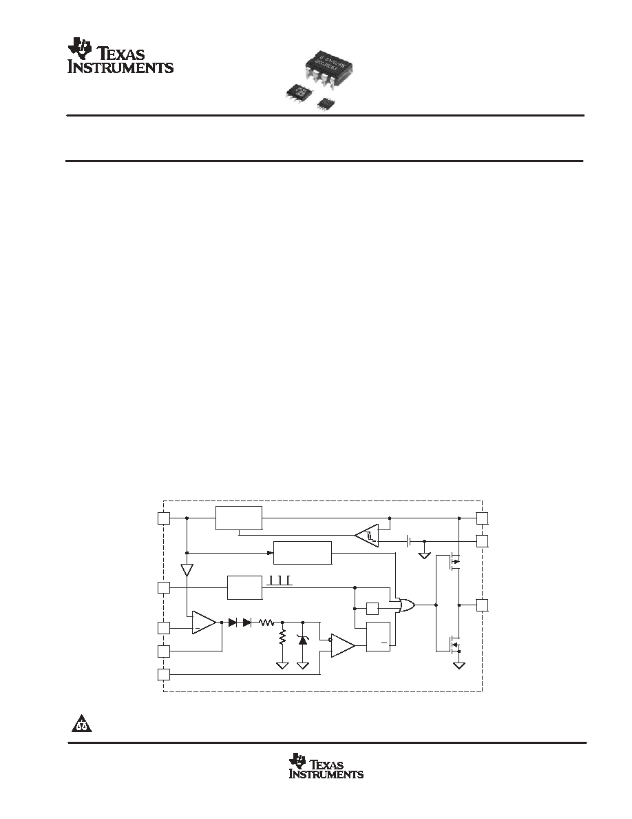
FUNCTIONAL BLOCK DIAGRAM
UDG-99139
8
2
4
7
VREF
Note: Toggle flip-flop used only in UCC38C41, UCC38C44, and UCC38C45.
VREF
RT/CT
+
VDD
5
GND
6
OUT
OSC
T
S
Q
Q
R
FB
2R
R
1V
1
COMP
3
CS
UVLO
ERROR AMP
(NOTE)
+
+
5.0 V
2.5 V
VREF
GOOD LOGIC
PRODUCTION DATA information is current as of publication date.
Products conform to specifications per the terms of Texas Instruments
standard warranty. Production processing does not necessarily include
testing of all parameters.
Copyright
2003, Texas Instruments Incorporated
Please be aware that an important notice concerning availability, standard warranty, and use in critical applications of Texas Instruments
semiconductor products and disclaimers thereto appears at the end of this data sheet.
UCC28C40, UCC28C41, UCC28C42, UCC28C43, UCC28C44, UCC28C45
UCC38C40, UCC38C41, UCC38C42, UCC38C43, UCC38C44, UCC38C45
SLUS458C - AUGUST 2001 - REVISED SEPTEMBER 2003
2
www.ti.com
recommended operating conditions
MIN
MAX
UNIT
Input voltage, VDD
18
V
Output voltage range, VOUT
18
V
Average output current, IOUT
W
200
mA
Reference output current, IOUT(ref)
W
-20
mA
Operating junction temperature, TJ
W
- 55
150
∞
C
∂ It is not recommended that the device operate under conditions beyond those specified in this table for extended periods of time.
absolute maximum ratings over operating free-air temperature (unless otherwise noted)
}w
Supply voltage (VDD)
20 V
. . . . . . . . . . . . . . . . . . . . . . . . . . . . . . . . . . . . . . . . . . . . . . . . . . . . . . . . . . . . . . . . . . . . . . .
(MAX ICC)
30 mA
. . . . . . . . . . . . . . . . . . . . . . . . . . . . . . . . . . . . . . . . . . . . . . . . . . . . . . . . . . . . . . . . . . .
Output current, I
OUT
peak
±
1 A
. . . . . . . . . . . . . . . . . . . . . . . . . . . . . . . . . . . . . . . . . . . . . . . . . . . . . . . . . . . . . . . . . . .
Output energy, capacitive load
5
µ
J
. . . . . . . . . . . . . . . . . . . . . . . . . . . . . . . . . . . . . . . . . . . . . . . . . . . . . . . . . . . . . . .
Voltage rating (COMP, CS, FB)
-0.3 V to 6.3 V
. . . . . . . . . . . . . . . . . . . . . . . . . . . . . . . . . . . . . . . . . . . . . . . . . . . . .
(OUT)
-0.3 V to 20 V
. . . . . . . . . . . . . . . . . . . . . . . . . . . . . . . . . . . . . . . . . . . . . . . . . . . . . . . . . . . . . . . .
(RT/CT)
-0.3 V to 6.3 V
. . . . . . . . . . . . . . . . . . . . . . . . . . . . . . . . . . . . . . . . . . . . . . . . . . . . . . . . . . . . .
(VREF)
7 V
. . . . . . . . . . . . . . . . . . . . . . . . . . . . . . . . . . . . . . . . . . . . . . . . . . . . . . . . . . . . . . . . . . . . . . . .
Error amplifier output sink current
10 mA
. . . . . . . . . . . . . . . . . . . . . . . . . . . . . . . . . . . . . . . . . . . . . . . . . . . . . . . . . . .
Total Power Dissipation at T
A
= 25
∞
C: D package (
jc = 22
∞
C/W,
ja = 40 - 70
∞
C/W)
650 mW
. . . . . . . . . .
DGK package (
jc = 41
∞
C/W,
ja = 238 - 269
∞
C/W
350 mW
. . . . . .
P package (
jc = 50
∞
C/W,
ja = 110
∞
C/W
850 mW
. . . . . . . . . . . . . .
Operating junction temperature range, T
J
-55
∞
C to 150
∞
C
. . . . . . . . . . . . . . . . . . . . . . . . . . . . . . . . . . . . . . . . . . . .
Storage temperature range T
stg
-65
∞
C to 150
∞
C
. . . . . . . . . . . . . . . . . . . . . . . . . . . . . . . . . . . . . . . . . . . . . . . . . . . .
Lead Temperature (Soldering, 10 seconds)
300
∞
C
. . . . . . . . . . . . . . . . . . . . . . . . . . . . . . . . . . . . . . . . . . . . . . . . . .
Stresses beyond those listed under "absolute maximum ratings" may cause permanent damage to the device. These are stress ratings only, and
functional operation of the device at these or any other conditions beyond those indicated under "recommended operating conditions" is not
implied. Exposure to absolute-maximum-rated conditions for extended periods may affect device reliability.
ß All voltages are with respect to ground. Currents are positive into and negative out of the specified terminals. Consult the Packaging Section of
the Databook for thermal limitations and considerations of the package.
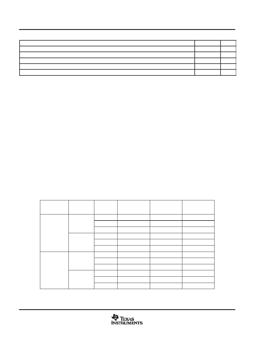
AVAILABLE OPTIONS
TA
MAXIMUM
DUTY CYCLE
UVLO
ON/OFF
SOIC-8
SMALL OUTLINE
(D)
{
PDIP-8
PLASTIC DIP
(P)
MSOP-8
SMALL OUTLINE
(DGK)
{
14.5V / 9.0V
UCC28C42D
UCC28C42P
UCC28C42DGK
100%
8.4V / 7.6V
UCC28C43D
UCC28C43P
UCC28C43DGK
-40
∞
C to 105
∞
C
100%
7.0V / 6.6V
UCC28C40D
UCC28C40P
UCC28C40DGK
-40
∞
C to 105
∞
C
14.5V / 9.0V
UCC28C44D
UCC28C44P
UCC28C44DGK
50%
8.4V / 7.6V
UCC28C45D
UCC28C45P
UCC28C45DGK
50%
7.0V / 6.6V
UCC28C41D
UCC28C41P
UCC28C41DGK
14.5V / 9.0V
UCC38C42D
UCC38C42P
UCC38C42DGK
100%
8.4V / 7.6V
UCC38C43D
UCC38C43P
UCC38C43DGK
0
∞
C to 70
∞
C
100%
7.0V / 6.6V
UCC38C40D
UCC38C40P
UCC38C40DGK
0 C to 70 C
14.5V / 9.0V
UCC38C44D
UCC38C44P
UCC38C44DGK
50%
8.4V / 7.6V
UCC38C45D
UCC38C45P
UCC38C45DGK
50%
7.0V / 6.6V
UCC38C41D
UCC38C41P
UCC38C41DGK
D (SOIC-8) and DGK (MSOP-8) packages are available taped and reeled. Add R suffix to device type (e.g.
UCC28C42DR) to order quantities of 2500 devices per reel. Tube quantities are 75 for D packages (SOIC-8) and
80 for DGK package (MSOP-8), and 50 for P package (PDIP-8).

UCC28C40, UCC28C41, UCC28C42, UCC28C43, UCC28C44, UCC28C45
UCC38C40, UCC38C41, UCC38C42, UCC38C43, UCC38C44, UCC38C45
SLUS458C - AUGUST 2001 - REVISED SEPTEMBER 2003
3
www.ti.com
electrical characteristics V
DD
= 15 V (See Note 1), R
T
= 10 k
, C
T
= 3.3 nF, C
VDD
= 0.1
µ
F and no load
on the outputs, T
A
= -40
∞
C to 105
∞
C for the UCC28C4x and T
A
= 0
∞
C to 70
∞
C for the UCC38C4x,
T
A
= T
J
(unless otherwise noted)
PARAMETER
TEST CONDITIONS
MIN
TYP
MAX
UNITS
Reference Section
Output voltage, initial accuracy
TA = 25
∞
C
IOUT = 1mA
4.9
5.0
5.1
V
Line regulation
VDD = 12 V to 18 V
0.2
20
mV
Load regulation
1mA to 20mA
3
25
mV
Temperature stability
See Note 2
0.2
0.4
mV/
∞
C
Total output variation
See Note 2
4.82
5.18
V
Output noise voltage
10 Hz to 10 kHz,
TA = 25
∞
C,
See Note 2
50
µ
V
Long term stability
1000 hours,
TA = 125
∞
C,
See Note 2
5
25
mV
Output short circuit
≠30
≠45
≠55
mA
Oscillator Section
Initial accuracy
TA = 25
∞
C,
See Note 3
50.5
53
55
kHz
Voltage stability
VDD = 12 V to 18 V
0.2%
1.0%
Temperature stability
TMIN to TMAX,
See Note 2
1%
2.5%
Amplitude
RT/CT Pin peak-to-peak
1.9
V
Discharge current
TA = 25
∞
C,
RT/CT = 2 V,
See Note 4
7.7
8.4
9.0
mA
Discharge current
RT/CT = 2 V,
See Note 4
7.2
8.4
9.5
mA
Error Amplifier Section
Feedback input voltage, initial accuracy
VCOMP = 2.5 V,
TA = 25
∞
C
2.475
2.500
2.525
V
Feedback input voltage, total variation
VCOMP = 2.5 V,
2.45
2.50
2.55
V
Input bias current
VFB = 5.0 V
≠0.1
≠2.0
µ
A
Open-loop voltage gain (AVOL)
VOUT = 2 V to 4 V
65
90
dB
Unity gain bandwidth
See Note 2
1.0
1.5
MHz
Power supply rejection ratio (PSRR)
VDD = 12 V to 18 V
60
dB
Output sink current
VFB = 2.7 V,
VCOMP = 1.1 V
2
14
mA
Output source current
VFB = 2.3 V,
VCOMP = 5V
≠0.5
≠1.0
mA
High-level output voltage (VOH)
VFB = 2.7 V,
RLOAD = 15 k to GND
5
6.8
V
Low-level output voltage (VOL)
VFB = 2.7 V,
RLOAD = 15 k to VREF
0.1
1.1
V
Current Sense Section
Gain
See Note 5, 6
2.85
3.00
3.15
V/V
Maximum input signal
VFB < 2.4 V
0.9
1.0
1.1
V
Power supply rejection ratio (PSRR)
VDD = 12 V to 18 V, See Note 2, 5
70
dB
Input bias current
≠0.1
≠2.0
µ
A
CS to output delay
35
70
ns
COMP to CS offset
VCS = 0 V
1.15
V
NOTE: 1. Adjust VDD above the start threshold before setting at 15 V.
NOTE: 2. Ensured by design. Not production tested.
NOTE: 3. Output frequencies of the UCC38C41, UCC38C44 and the UCC38C45 are half the oscillator frequency.
NOTE: 4. Oscillator discharge current is measured with RT = 10 k
to VREF.
NOTE: 5. Parameter measured at trip point of latch with VFB = 0 V.
NOTE: 6. Gain is defined as ACS
+
D
V
COM
D
V
CS
, 0V
¨
V
CS
¨
900mV
UCC28C40, UCC28C41, UCC28C42, UCC28C43, UCC28C44, UCC28C45
UCC38C40, UCC38C41, UCC38C42, UCC38C43, UCC38C44, UCC38C45
SLUS458C - AUGUST 2001 - REVISED SEPTEMBER 2003
4
www.ti.com
electrical characteristics V
DD
= 15 V (See Note 1), R
T
= 10 k
, C
T
= 3.3 nF, C
VDD
= 0.1
µ
F and no load
on the outputs, T
A
= -40
∞
C to 105
∞
C for the UCC28C4x and T
A
= 0
∞
C to 70
∞
C for the UCC38C4x,
T
A
= T
J
(unless otherwise noted)
PARAMETER
TEST CONDITIONS
MIN
TYP
MAX
UNITS
Output Section
VOUT low (RDS(on) pull-down)
ISINK = 200 mA
5.5
15
VOUThigh (RDS(on) pull-up)
ISOURCE = 200 mA
10
25
Rise tIme
TA = 25
∞
C, CLOAD = 1 nF
25
50
ns
Fall time
TA = 25
∞
C, CLOAD = 1 nF
20
40
ns
Undervoltage Lockout Section
UCC38C42, UCC38C44
13.5
14.5
15.5
Start threshold
UCC38C43, UCC38C45
7.8
8.4
9.0
Start threshold
UCC38C40, UCC38C41
6.5
7.0
7.5
V
UCC38C42, UCC38C44
8
9
10
V
Minimum operating voltage
UCC38C43, UCC38C45
7.0
7.6
8.2
Minimum operating voltage
UCC38C40, UCC38C41
6.1
6.6
7.1
PWM Section
Maximum duty cycle
UCC38C42, UCC38C43, UCC38C40, VFB < 2.4 V
94%
96%
Maximum duty cycle
UCC38C44, UCC38C45, UCC38C41, VFB < 2.4 V
47%
48%
Minimum duty cycle
VFB > 2.6 V
0%
Current Supply Section
Start-up current (ISTART-UP)
VDD = Undervoltage lockout start threshold (-0.5 V)
50
100
µ
A
Operating supply current (IDD)
VFB = VCS = 0 V
2.3
3.0
mA
NOTE 1: Adjust VDD above the start threshold before setting at 15 V.
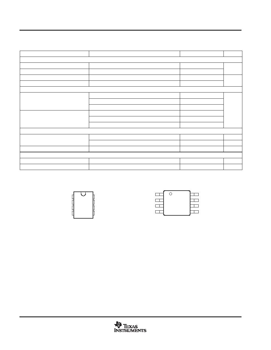
1
2
3
4
8
7
6
5
COMP
FB
CS
RT/CT
VREF
VDD
OUT
GND
PDIP (P) or SOIC (D) PACKAGE
(TOP VIEW)
MSOP (DGK) PACKAGE
(TOP VIEW)
VREF
VDD
OUT
GND
8
7
6
5
1
2
3
4
COMP
FB
CS
RT/CT

UCC28C40, UCC28C41, UCC28C42, UCC28C43, UCC28C44, UCC28C45
UCC38C40, UCC38C41, UCC38C42, UCC38C43, UCC38C44, UCC38C45
SLUS458C - AUGUST 2001 - REVISED SEPTEMBER 2003
5
www.ti.com
pin assignments
COMP: This pin provides the output of the error amplifier for compensation. In addition, the COMP pin is
frequently used as a control port by utilizing a secondary-side error amplifier to send an error signal across the
secondary-primary isolation boundary through an opto-isolator.
CS: The current sense pin is the non-inverting input to the PWM comparator. This is compared to a signal
proportional to the error amplifier output voltage. A voltage ramp can be applied to this pin to run the device with
a voltage mode control configuration.
FB: This pin is the inverting input to the error amplifier. The non-inverting input to the error amplifier is internally
trimmed to 2.5 V
±
1%.
GND: Ground return pin for the output driver stage and the logic level controller section.
OUT: The output of the on-chip drive stage. OUT is intended to directly drive a MOSFET. The OUT pin in the
UCC38C40, UCC38C42 and UCC38C43 is the same frequency as the oscillator, and can operate near 100%
duty cycle. In the UCC38C41, UCC38C44 and the UCC38C45, the frequency of OUT is one-half that of the
oscillator due to an internal T flipflop. This limits the maximum duty cycle to < 50%.
RT/CT: Timing resistor and timing capacitor. The timing capacitor should be connected to the device ground
using minimal trace length.
VDD: Power supply pin for the device. This pin should be bypassed with a 0.1-
µ
F capacitor with minimal trace
lengths. Additional capacitance may be needed to provide hold up power to the device during startup.
VREF: 5-V reference. For stability, the reference should be bypassed with a 0.1-
µ
F capacitor to ground using
the minimal trace length possible.

UCC28C40, UCC28C41, UCC28C42, UCC28C43, UCC28C44, UCC28C45
UCC38C40, UCC38C41, UCC38C42, UCC38C43, UCC38C44, UCC38C45
SLUS458C - AUGUST 2001 - REVISED SEPTEMBER 2003
6
www.ti.com
APPLICATION INFORMATION
This device is a pin-for-pin replacement of the bipolar UC3842 family of controllers, the industry standard PWM
controller for single-ended converters. Familiarity with this controller family is assumed.
The UCC28C4x/UCC38C4x series is an enhanced replacement with pin-to-pin compatibility to the bipolar
UC284x/UC384x and UC284xA/UC384xA families. The new series offers improved performance when
compared to older bipolar devices and other competitive BiCMOS devices with similar functionality. Note that
these improvements discussed below generally consist of tighter specification limits that are a subset of the
older product ratings, maintaining drop-in capability. In new designs these improvements can be utilized to
reduce the component count or enhance circuit performance when compared to the previously available
devices.
advantages
This device increases the total circuit efficiency whether operating off-line or in dc input circuits. In off-line
applications the low start-up current of this device reduces steady state power dissipation in the startup resistor,
and the low operating current maximizes efficiency while running. The low running current also provides an
efficiency boost in battery operated supplies.
low voltage operation
Two members of the UCC38C4x family are intended for applications that require a lower start-up voltage than
the original family members. The UCC38C40 and UCC38C41 have a turn-on voltage of 7.0 V typical and exhibit
hysteresis of 0.4 V for a turn-off voltage of 6.6 V. This reduced start-up voltage enables use in systems with lower
voltages, such as 12-V battery systems which are nearly discharged.
high speed operation
The BiCMOS design allows operation at high frequencies that were not feasible in the predecessor bipolar
devices. First, the output stage has been redesigned to drive the external power switch in approximately half
the time of the earlier devices. Second, the internal oscillator is more robust with less variation as frequency
increases. In addition, the current sense to output delay has been reduced by a factor of three, to 45ns typical.
These features combine to provide a device capable of reliable high frequency operation.
The UCC38C4x family oscillator is true to the curves of the original bipolar devices at lower frequencies yet
extends the frequency programmability range to at least 1MHz. This allows the device to offer pin to pin
capability where required yet capable of extending the operational range to the higher frequencies typical of
latest applications. When the original UC3842 was released in 1984 most switching supplies operated between
20kHz and 100kHz. Today, the UCC38C4x can be used in designs cover a span roughly ten times higher than
those numbers.
start/run current improvements
The start-up current is only 60
µ
A typical, a significant reduction from the bipolar device's ratings of 300uA
(UC384xA). For operation over the temperature range of -40 to 85
∞
C the UCC28C4x devices offer a maximum
startup current of 100
µ
A, an improvement over competitive BiCMOS devices. This allows the power supply
designer to further optimize the selection of the startup resistor value to provide a more efficient design. In
applications where low component cost overrides maximum efficiency the low run current of 2.3 mA, typical,
may allow the control device to run directly through the single resistor to (+) rail, rather than needing a bootstrap
winding on the power transformer, along with a rectifier. The start/run resistor for this case must also pass
enough current to allow driving the primary switching MOSFET, which may be a few milliamps in small devices.

UCC28C40, UCC28C41, UCC28C42, UCC28C43, UCC28C44, UCC28C45
UCC38C40, UCC38C41, UCC38C42, UCC38C43, UCC38C44, UCC38C45
SLUS458C - AUGUST 2001 - REVISED SEPTEMBER 2003
7
www.ti.com
APPLICATION INFORMATION
±
1% initial reference voltage
The BiCMOS internal reference of 2.5 V has an enhanced design and utilizes production trim to allow initial
accuracy of
±
1% at room temperature and
±
2% over the full temperature range. This can be used to eliminate
an external reference in applications that do not require the extreme accuracy afforded by the additional device.
This is very useful for nonisolated dc-to-dc applications where the control device is referenced to the same
common as the output. It is also applicable in offline designs that regulate on the primary side of the isolation
boundary by looking at a primary bias winding, or perhaps from a winding on the output inductor of a
buck-derived circuit.
reduced discharge current variation
The original UC3842 oscillator did not have trimmed discharged current, and the parameter was not specified
on the datasheet. Since many customers attempted to use the discharge current to set a crude deadtime limit
the UC3842A family was released with a trimmed discharge current specified at 25
∞
C. The
UCC28C4x/UCC38C4x series now offers even tighter control of this parameter, with approximately
±
3%
accuracy at 25
∞
C, and less than 10% variation over temperature using the UCC28C4x devices. This level of
accuracy can enable a meaningful limit to be programmed, a feature not currently seen in competitive BiCMOS
devices. The improved oscillator and reference also contribute to decreased variation in the peak to peak
variation in the oscillator waveform, which is often used as the basis for slope compensation for the complete
power system.
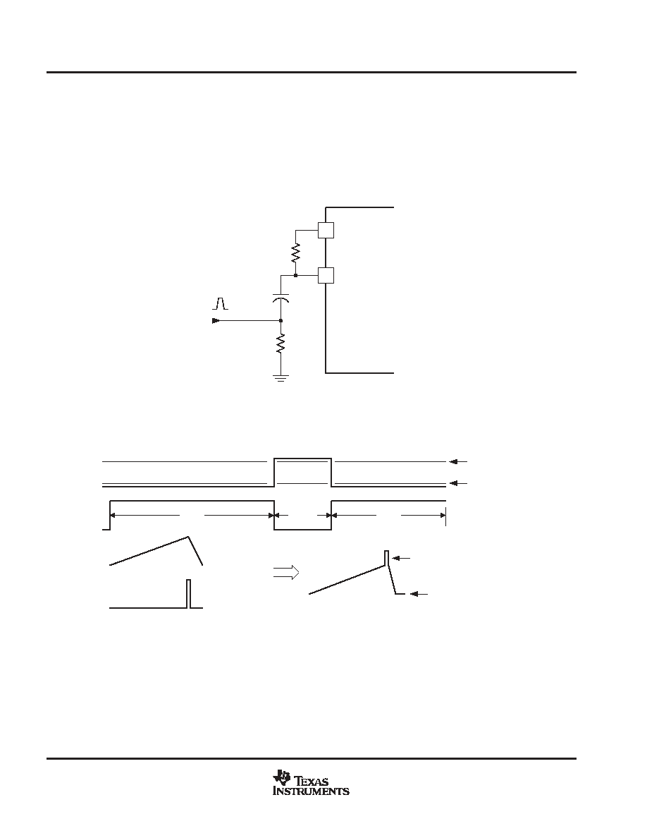
soft-start
The following diagram provides a typical soft-start circuit for use with the UCC38C42. The values of R and C
should be selected to bring the COMP pin up at a controlled rate, limiting the peak current supplied by the power
stage. After the soft-start interval is complete the capacitor continues to charge to V
REF
, effectively removing
the PNP transistor from circuit considerations.
The optional diode in parallel with the resistor forces a soft-start each time the PWM goes through UVLO and
the reference (V
REF
) goes low. Without the diode,the capacitor otherwise remains charged during a brief loss
of supply or brown-out, and no soft-start is enabled upon reapplication of VIN.
Figure 1
UDG-01072
VREF
UCC38C42
8
1
COMP
5
GND
UCC28C40, UCC28C41, UCC28C42, UCC28C43, UCC28C44, UCC28C45
UCC38C40, UCC38C41, UCC38C42, UCC38C43, UCC38C44, UCC38C45
SLUS458C - AUGUST 2001 - REVISED SEPTEMBER 2003
8
www.ti.com
APPLICATION INFORMATION
oscillator synchronization
The UCC38C4x oscillator has the same synchronization characteristics as the original bipolar devices. Thus,
the information in the Application Note U-100A, UC3842/3/4/5 Provides Low-Cost Current-Mode Control, (TI
Literature No. SLUA143) still applies. The application note describes how a small resistor from the timing
capacitor-to-ground can offer an insertion point for synchronization to an external clock, (see Figures 2 and 3).
Figure 2 shows how the UCC38C42 can be synchronized to an external clock source. This allows precise
control of frequency and dead time with a digital pulse train.
UDG-01069
8
4
VREF
RT/ CT
UCC38C42
PWM
RT
CT
24
W
SYNCHRONIZATION
CIRCUIT INPUT
Figure 2. Oscillator Synchronization Circuit
ON
.
LOW
LOW
HIGH
ON
.
OFF
.
CLOCK
INPUT
PWM
OUT
UPPER THRESHOLD
LOWER THRESHOLD
OUTPUT A
COMBINED
UPPER THRESHOLD
LOWER THRESHOLD
V
CT
V
CT
(ANALOG)
V
SYNC
(DIGITAL)
UDG-01070
Figure 3. Synchronization to an External Clock
UCC28C40, UCC28C41, UCC28C42, UCC28C43, UCC28C44, UCC28C45
UCC38C40, UCC38C41, UCC38C42, UCC38C43, UCC38C44, UCC38C45
SLUS458C - AUGUST 2001 - REVISED SEPTEMBER 2003
9
www.ti.com
APPLICATION INFORMATION
precautions
The absolute maximum supply voltage is 20 V, including any transients that may be present. If this voltage is
exceeded, device damage is likely. This is in contrast to the predecessor bipolar devices, which could survive
up to 30 V. Thus, the supply pin should be decoupled as close to the ground pin as possible. Also, since no clamp
is included in the device, the supply pin should be protected from external sources which could exceed the 20 V
level.
Careful layout of the printed board has always been a necessity for high frequency power supplies. As the device
switching speeds and operating frequencies increase the layout of the converter becomes increasingly
important.
This 8-pin device has only a single ground for the logic and power connections. This forces the gate drive current
pulses to flow through the same ground that the control circuit uses for reference. Thus, the interconnect
inductance should be minimized as much as possible. One implication is to place the device (gate driver)
circuitry close to the MOSFET it is driving. Note that this can conflict with the need for the error amplifier and
the feedback path to be away from the noise generating components.
circuit applications
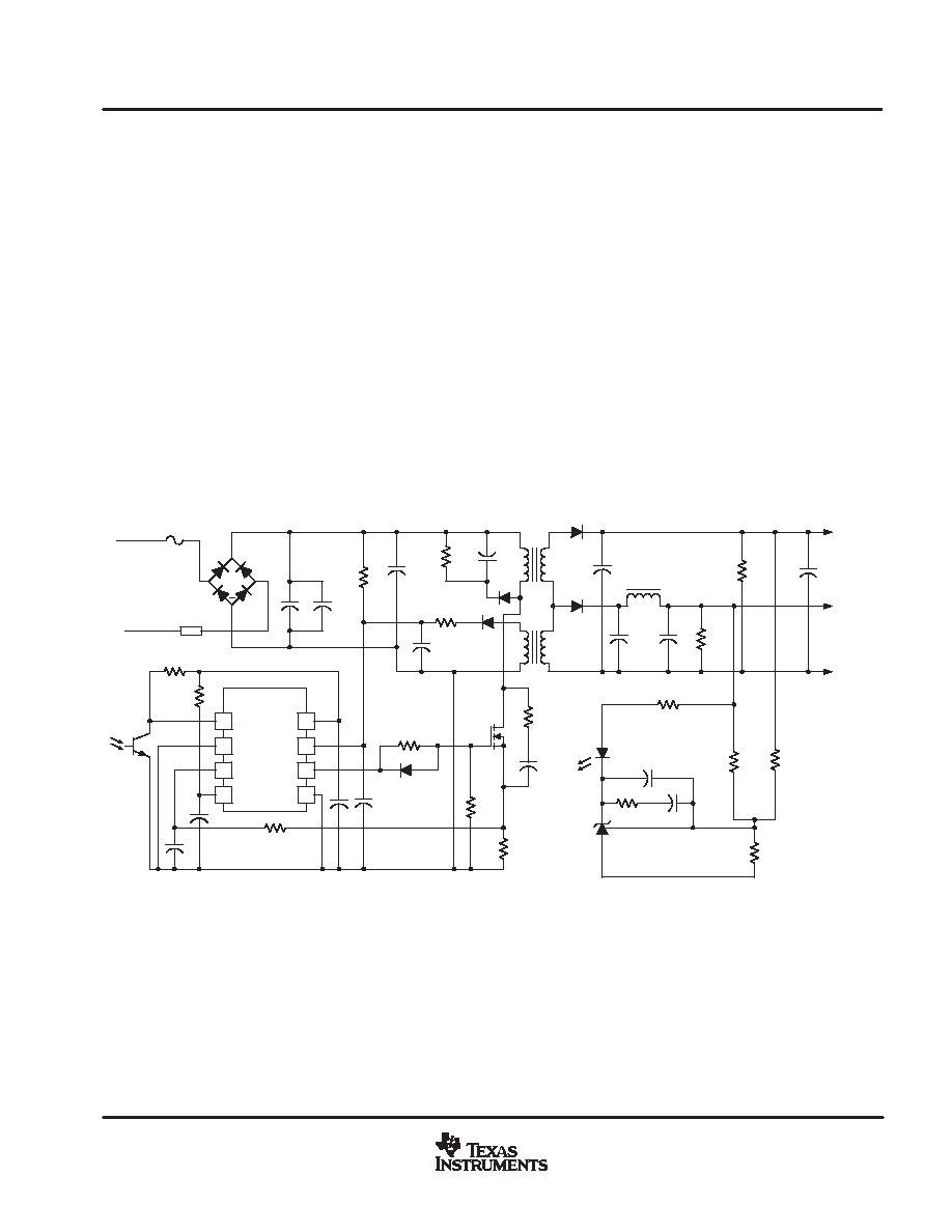
Figure 4 shows a typical off-line application.
UDG-01071
C53
1
COMP
2
FB
3
CS
4
RT/CT
8
REF
7
VCC
6
OUT
5
GND
UCC38C44
R6
C13
R16
T1
R12
C5
C12
D50
C52
D51
C3
R10
R11
C18
C1A
F1
BR1
+
RT1
L50
C54
R55
R53
R56
C55
R52
SEC
COMMON
12 V
OUT
R50
C50
C51
R50
IC3
R54
A
R
K
Q1
5 V
OUT
AC INPUT
100 Vac - 240 Vac
EMI FILTER
REQUIRED
D2
D6
IC2
IC2
Figure 4. Typical Off-Line Application
Figure 5 shows the forward converter with synchronous rectification. This application provides 48 V to 3.3 V at
10 A with over 85% efficiency and uses the UCC38C42 as the secondary-side controller and UCC3961 as the
primary-side startup control device.
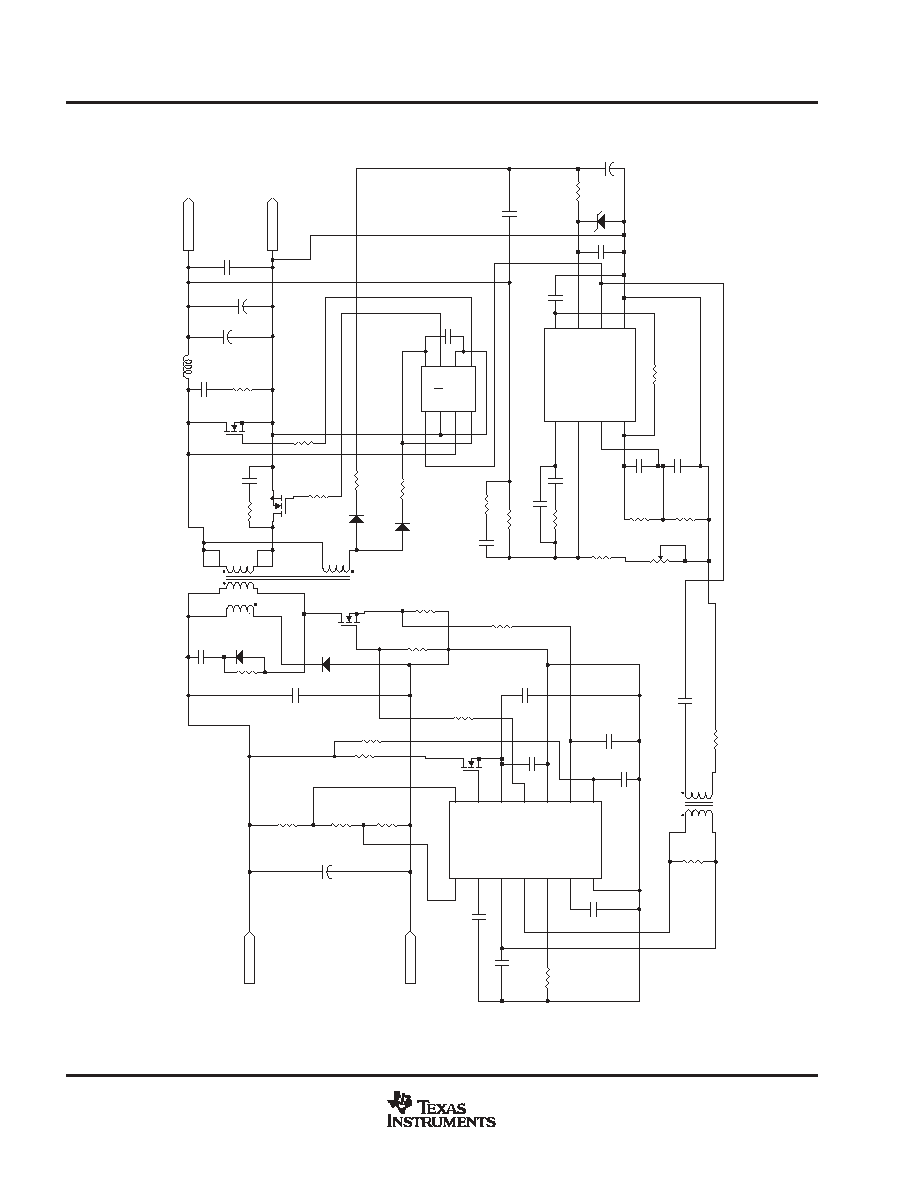
UCC28C40, UCC28C41, UCC28C42, UCC28C43, UCC28C44, UCC28C45
UCC38C40, UCC38C41, UCC38C42, UCC38C43, UCC38C44, UCC38C45
SLUS458C - AUGUST 2001 - REVISED SEPTEMBER 2003
10
www.ti.com
APPLICATION INFORMATION
R28
100
D3
BAR74
C26
2uF
D5
BAR74
R14
20k 40%
C16
5.6nF
+
C15
1uF
C14
1uF
C13
0.22uF
C12
3300pF
C11
1500pF
D6
BZX84C15LT1
UCC38C4x
1
COMP
2
FB
3
CS
4
Rt/Ct
5
GND
6
OUT
7
Vcc
8
REF
U2
C22
4.7nF
C23
680pF
C24
0.1uF
C10
2.7nF
1
2
3
4
T2
Q4
Q3
L1
4.7uH
C21
0.1uF
+
C20
470uF
+
C19
470uF
3r3V
PWRGND
D2
C2
1nF
C18
4700pF
C25
0.047uF
VinN
VinP
C9
0.1uF
ucc3961
4
FB
5
Rt
6
Ref
7
AGnd
8
Vs
9
CS
10
PGnd
11
Out
1
OVS
2
SD
3
SS
12
Vdd
13
St
14
UVS
U1
+
C1
470uF
C3
10nF
C4
0.22uF
C5
0.1uF
C6
470pF
C7
100pF
C8
1uF
C17
4700pF
D1
Q1
Q2
TPS2832
8
BOOT
1
IN
6
BTLO
3
DT
7
HIDR
4
Vcc
2
PGND
5
LODR
U4
T1
R19
20
R22
100
R18
7.5k
R17
20k
R16
21.5k
R15
50k
R23
402
R24
20k
R25
20k
R12
200
R13
300
R27
4.7
R26
4.7
R7
10k
R21
10
R1
32.4k
R2
1.2k
R3
2.4k
R4
1.5k
R5
76.8k
R6
4.7
R8
5.1k
R9
0.33
R10
1k
R11
46.4k
R20
10
Figure 5. Forward Converter with Synchronous Rectification Using the UCC38C42
as the Secondary-Side Controller
UCC28C40, UCC28C41, UCC28C42, UCC28C43, UCC28C44, UCC28C45
UCC38C40, UCC38C41, UCC38C42, UCC38C43, UCC38C44, UCC38C45
SLUS458C - AUGUST 2001 - REVISED SEPTEMBER 2003
11
www.ti.com
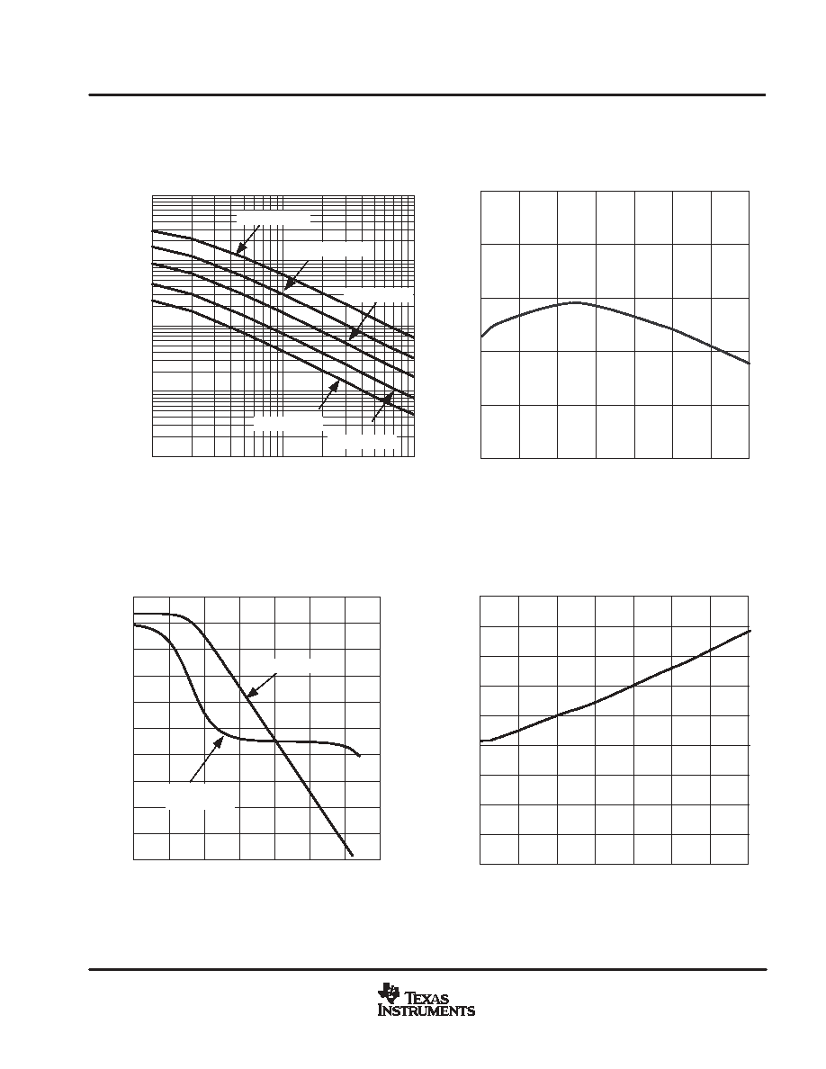
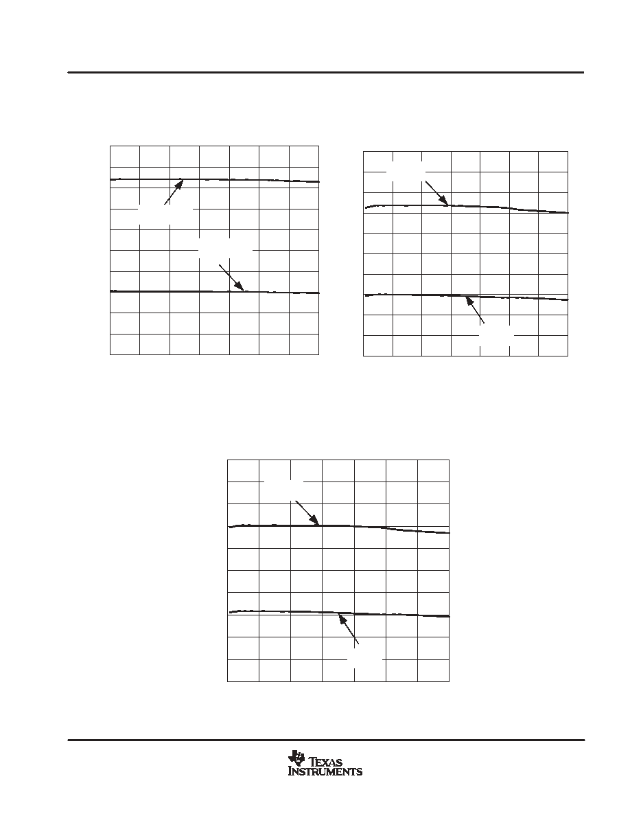
TYPICAL CHARACTERISTICS
1 k
10 k
100 k
1 k
10 k
100 k
1 M
10 M
Figure 6
OSCILLATOR FREQUENCY
vs
TIMING RESISTANCE AND CAPACITANCE
CT = 220 pF
CT = 4.7 nF
CT = 2.2 nF
CT = 1 nF
CT = 470 pF
RT - Timing Resistance -
W
f - Frequency - Hz
Figure 7
I DISCH
- Oscillator Discharge Current - mA
TJ - Temperature -
∞
C
9.0
9.5
8.0
7.5
7.0
8.5
-50
-25
0
25
50
75
100
125
OSCILLATOR DISCHARGE CURRENT
vs
TEMPERATURE
Figure 8
f - Frequency - Hz
Gain - (dB)
ERROR AMPLIFIER
FREQUENCY RESPONSE
1
10
100
10 k
100 k
1 M
10 M
1 k
10
0
20
200
180
140
120
80
40
0
60
100
160
20
30
40
50
60
70
80
90
100
Phase
Margin - (
∞
)
GAIN
PHASE
MARGIN
Figure 9
COMP to CS OFFSET VOLTAGE (with CS = 0)
vs
TEMPERATURE
COMP to CS
TJ - Temperature -
∞
C
0.2
1.8
1.4
1.2
0.8
0.4
0.0
0.6
1.0
1.6
-50
-25
0
25
50
75
100
125
UCC28C40, UCC28C41, UCC28C42, UCC28C43, UCC28C44, UCC28C45
UCC38C40, UCC38C41, UCC38C42, UCC38C43, UCC38C44, UCC38C45
SLUS458C - AUGUST 2001 - REVISED SEPTEMBER 2003
12
www.ti.com
TYPICAL CHARACTERISTICS
Figure 10
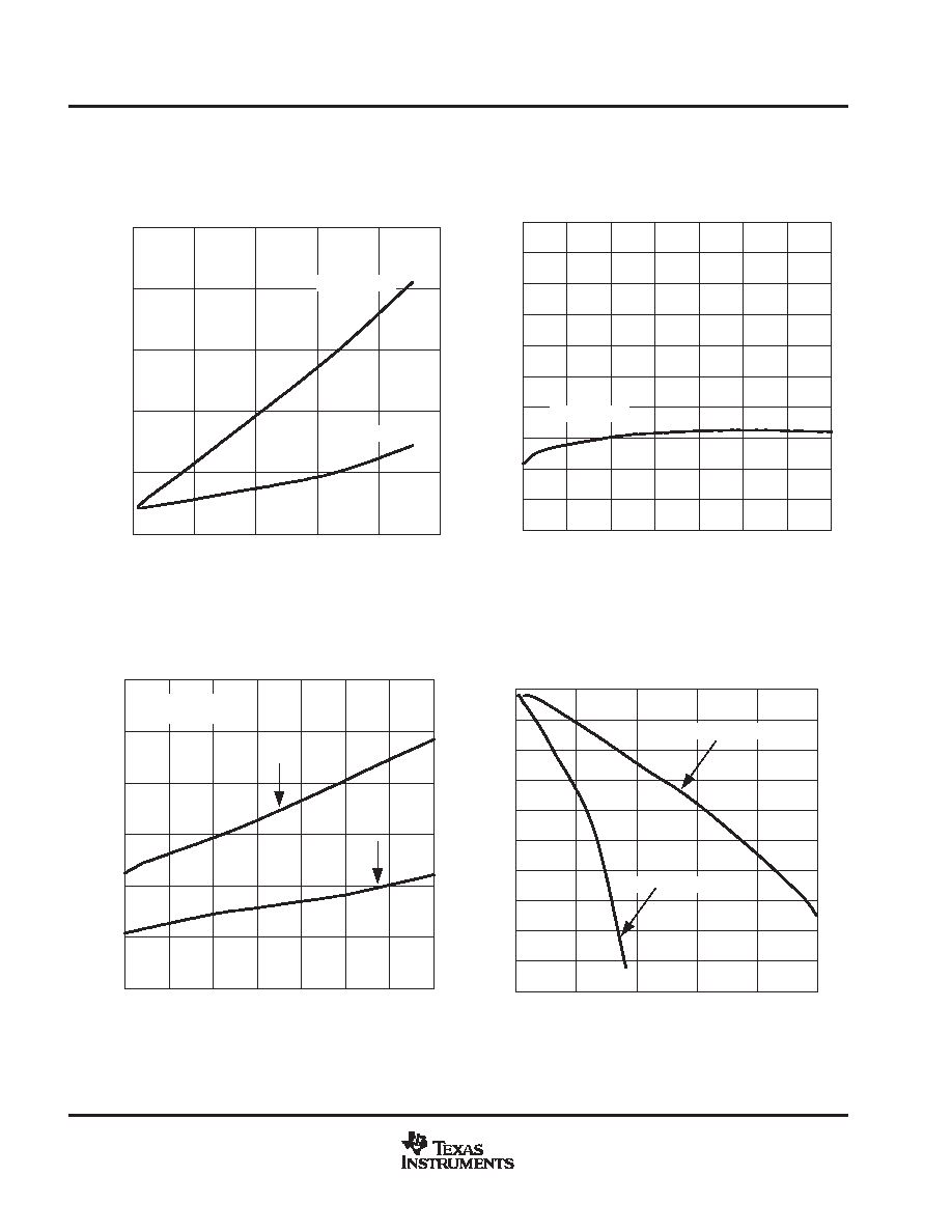
REFERENCE VOLTAGE
vs
TEMPERATURE
V
REF
- Reference V
o
ltage - V
-50
-25
0
25
50
75
100
125
TJ - Temperature -
∞
C
4.96
4.97
4.98
4.99
5.01
5.02
5.03
5.04
5.05
5.00
4.95
2.46
2.55
2.54
2.52
2.51
2.49
2.47
2.45
2.48
2.50
2.53
-50
-25
0
25
50
75
100
125
ERROR AMPLIFIER REFERENCE VOLTAGE
vs
TEMPERATURE
Figure 11
V
EAREF
- Error Amplifier Reference V
oltage - V
TJ - Temperature -
∞
C
Figure 12
I SC
- Reference Short Circuit Current - mA
REFERENCE SHORT-CIRCUIT CURRENT
vs
TEMPERATURE
-55
-35
-37
-41
-45
-51
-53
-47
-49
-43
-39
-50
-25
0
25
50
75
100
125
TJ - Temperature -
∞
C
-200
200
150
50
0
-50
-150
100
-100
ERROR AMPLIFIER INPUT BIAS CURRENT
vs
TEMPERATURE
Figure 13
I BIAS
- Error Amplifier Input Bias Current - nA
TJ - Temperature -
∞
C
-50
-25
0
25
50
75
100
125
UCC28C40, UCC28C41, UCC28C42, UCC28C43, UCC28C44, UCC28C45
UCC38C40, UCC38C41, UCC38C42, UCC38C43, UCC38C44, UCC38C45
SLUS458C - AUGUST 2001 - REVISED SEPTEMBER 2003
13
www.ti.com
TYPICAL CHARACTERISTICS
Figure 14
6
16
15
13
11
8
7
10
9
12
14
-50
-25
0
25
50
75
100
125
UVLO
ON
UVLO
OFF
UNDERVOLTAGE LOCKOUT
vs
TEMPERATURE (UCC38C42 & UCC38C44)
V
UVLO
- UVLO V
o
ltage - V
TJ - Temperature -
∞
C
Figure 15
UNDERVOLTAGE LOCKOUT
vs
TEMPERATURE (UCC38C43 & UCC38C45)
V
UVLO
- UVLO V
o
ltage - V
TJ - Temperature -
∞
C
7.0
9.0
8.8
8.4
8.0
7.4
7.2
7.8
7.6
8.2
8.6
-50
-25
0
25
50
75
100
125
UVLO
ON
UVLO
OFF
6.3
7.3
7.2
7.0
6.8
6.5
6.4
6.7
6.6
7.1
-50
-25
0
25
50
75
100
125
6.9
Figure 16
UNDERVOLTAGE LOCKOUT
vs
TEMPERATURE (UCC38C40 & UCC38C41)
V
UVLO
- UVLO V
o
ltage - V
TJ - Temperature -
∞
C
UVLO
ON
UVLO
OFF
UCC28C40, UCC28C41, UCC28C42, UCC28C43, UCC28C44, UCC28C45
UCC38C40, UCC38C41, UCC38C42, UCC38C43, UCC38C44, UCC38C45
SLUS458C - AUGUST 2001 - REVISED SEPTEMBER 2003
14
www.ti.com
TYPICAL CHARACTERISTICS
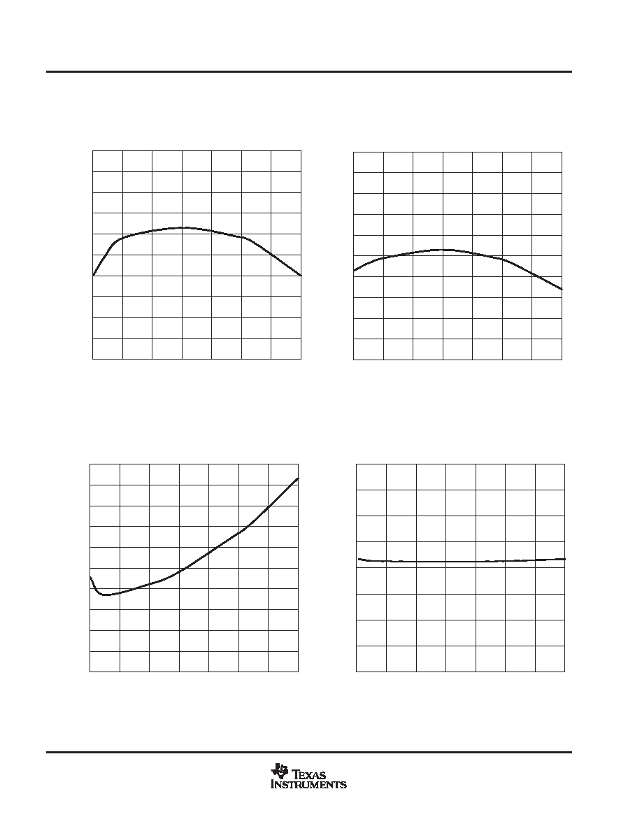
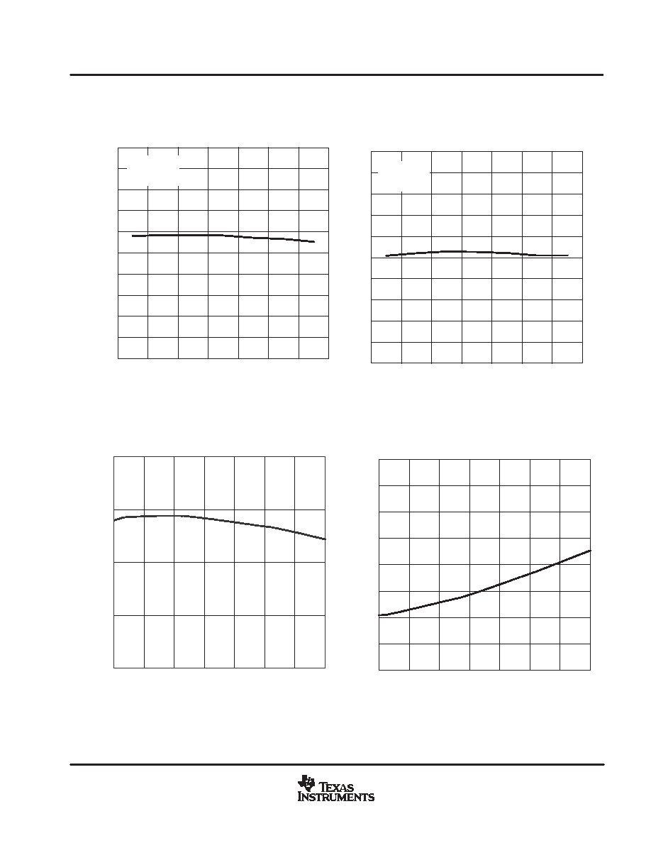
Figure 17
5
0
10
15
20
25
200 k
400 k
600 k
800 k
0 k
1 M
1-nF LOAD
NO LOAD
SUPPLY CURRENT
vs
OSCILLATOR FREQUENCY
I DD
- Supply Current - mA
f - Frequency - Hz
Figure 18
I DD
- Supply Current - mA
-50
2.1
3.0
2.9
2.7
2.6
2.4
2.2
2.0
2.3
2.5
2.8
-25
0
25
50
75
100
125
SUPPLY CURRENT
vs
TEMPERATURE
TJ - Temperature -
∞
C
NO LOAD
Figure 19
OUTPUT RISE TIME AND FALL TIME
vs
TEMPERATURE
Output Rise and Fall TIme - ns
10
15
40
35
30
20
25
tf
tr
(1 nF)
-50
-25
0
25
50
75
100
125
TJ - Temperature -
∞
C
(1 nF)
10% to 90%
VDD = 12 V
Figure 20
Duty Cycle - %
f - Frequency - kHz
MAXIMUM DUTY CYCLE
vs
OSCILLATOR FREQUENCY
50
100
90
60
0
500
80
70
CT = 220 pF
CT = 1 nF
1000
1500
2000
2500
UCC28C40, UCC28C41, UCC28C42, UCC28C43, UCC28C44, UCC28C45
UCC38C40, UCC38C41, UCC38C42, UCC38C43, UCC38C44, UCC38C45
SLUS458C - AUGUST 2001 - REVISED SEPTEMBER 2003
15
www.ti.com
TYPICAL CHARACTERISTICS
Figure 21
Maximum
Duty Cycle - %
MAXIMUM DUTY CYCLE
vs
TEMPERATURE
90
100
92
94
96
98
-50
-25
0
25
50
75
100
125
UCC38C40
UCC38C42
UCC38C43
TJ - Temperature -
∞
C
Figure 22
MAXIMUM DUTY CYCLE
vs
TEMPERATURE
Output Rise and Fall TIme - ns
45
50
46
47
48
49
-50
-25
0
25
50
75
100
125
UCC38C41
UCC38C44
UCC38C45
TJ - Temperature -
∞
C
Figure 23
CURRENT SENSE THRESHOLD VOLTAGE
vs
TEMPERATURE
V
CS_th
- Current Sense Threshold - V
0.90
0.95
1.00
1.05
1.10
-50
-25
0
25
50
75
100
125
TJ - Temperature -
∞
C
Figure 24
t D
- CD to OUT Delay T
ime - ns
CS TO OUT DELAY TIME
vs
TEMPERATURE
30
-50
-25
0
25
50
75
100
125
35
70
65
60
55
45
40
50
TJ - Temperature -
∞
C
UCC28C40, UCC28C41, UCC28C42, UCC28C43, UCC28C44, UCC28C45
UCC38C40, UCC38C41, UCC38C42, UCC38C43, UCC38C44, UCC38C45
SLUS458C - AUGUST 2001 - REVISED SEPTEMBER 2003
16
www.ti.com
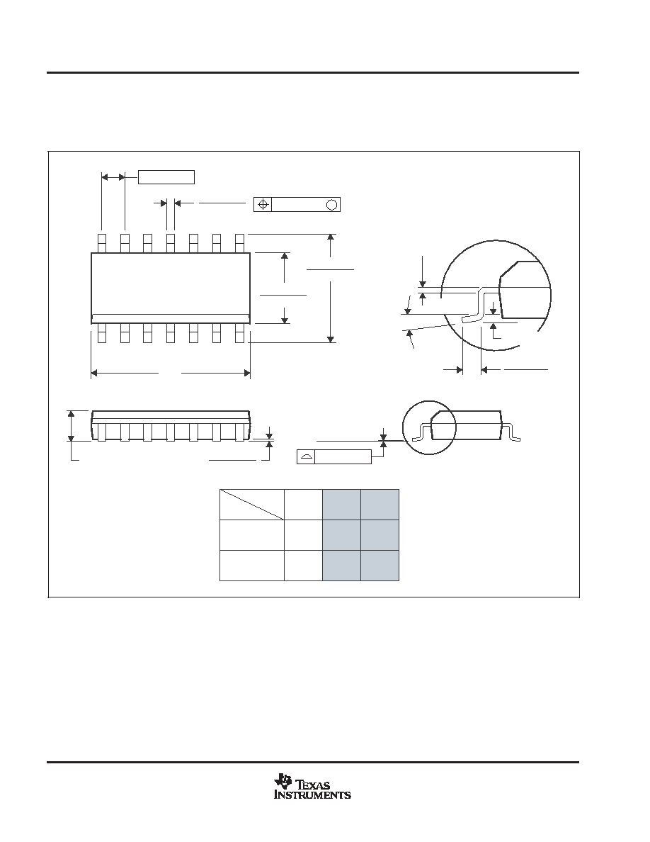
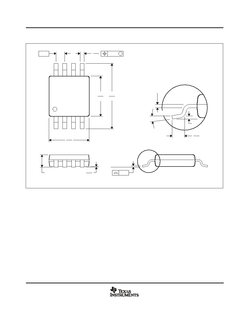
MECHANICAL DATA
D (SOIC)
PLASTIC SMALL-OUTLINE PACKAGE
Note: UCC38C4x is offered in an 8-pin package ONLY.
14 PINS SHOWN
4040047 / D 10/96
0.228 (5,80)
0.244 (6,20)
0.069 (1,75) MAX
0.010 (0,25)
0.004 (0,10)
1
14
0.014 (0,35)
0.020 (0,51)
A
0.157 (4,00)
0.150 (3,81)
7
8
0.044 (1,12)
0.016 (0,40)
Seating Plane
0.010 (0,25)
PINS **
0.008 (0,20) NOM
A MIN
A MAX
DIM
Gage Plane
0.189
(4,80)
(5,00)
0.197
8
(8,55)
(8,75)
0.337
14
0.344
(9,80)
16
0.394
(10,00)
0.386
0.004 (0,10)
M
0.010 (0,25)
0.050 (1,27)
0
∞
- 8
∞
NOTES: A. All linear dimensions are in inches (millimeters).
B. This drawing is subject to change without notice.
C. Body dimensions do not include mold flash or protrusion, not to exceed 0.006 (0,15).
D. Falls within JEDEC MS-012
UCC28C40, UCC28C41, UCC28C42, UCC28C43, UCC28C44, UCC28C45
UCC38C40, UCC38C41, UCC38C42, UCC38C43, UCC38C44, UCC38C45
SLUS458C - AUGUST 2001 - REVISED SEPTEMBER 2003
17
www.ti.com
MECHANICAL DATA
DGK (R-PDSO-G8)
PLASTIC SMALL-OUTLINE PACKAGE
0,69
0,41
0,25
0,15 NOM
Gage Plane
4073329/B 04/98
4,98
0,25
5
3,05
4,78
2,95
8
4
3,05
2,95
1
0,38
1,07 MAX
Seating Plane
0,65
M
0,25
0
∞
- 6
∞
0,10
0,15
0,05
NOTES: A. All linear dimensions are in millimeters.
B. This drawing is subject to change without notice.
C. Body dimensions do not include mold flash or protrusion.
D. Falls within JEDEC MO-187
UCC28C40, UCC28C41, UCC28C42, UCC28C43, UCC28C44, UCC28C45
UCC38C40, UCC38C41, UCC38C42, UCC38C43, UCC38C44, UCC38C45
SLUS458C - AUGUST 2001 - REVISED SEPTEMBER 2003
18
www.ti.com
MECHANICAL DATA
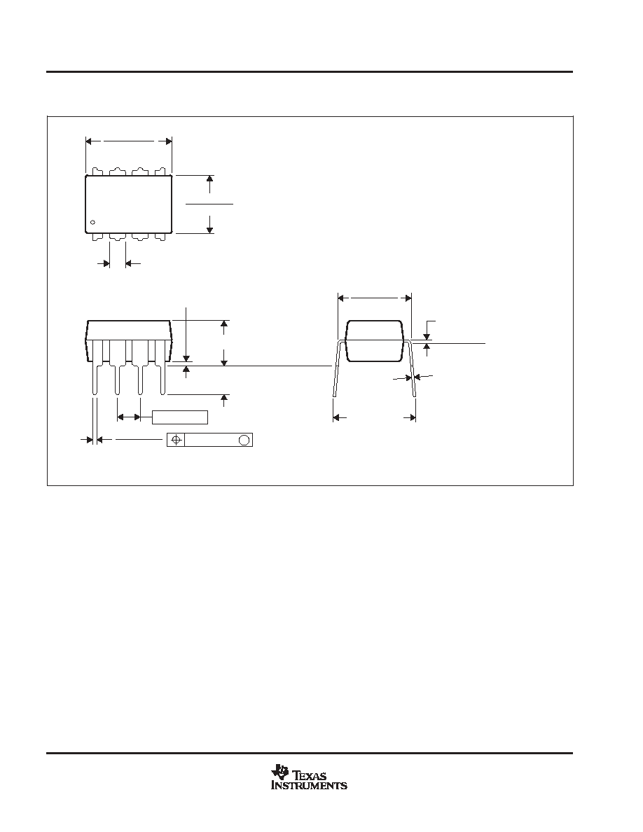
P (PDIP)
PLASTIC DUAL-IN-LINE
8
4
0.015 (0,38)
Gage Plane
0.325 (8,26)
0.300 (7,62)
0.010 (0,25) NOM
MAX
0.430 (10,92)
4040082/D 05/98
0.200 (5,08) MAX
0.125 (3,18) MIN
5
0.355 (9,02)
0.020 (0,51) MIN
0.070 (1,78) MAX
0.240 (6,10)
0.260 (6,60)
0.400 (10,60)
1
0.015 (0,38)
0.021 (0,53)
Seating Plane
M
0.010 (0,25)
0.100 (2,54)
NOTES: A. All linear dimensions are in inches (millimeters).
B. This drawing is subject to change without notice.
C. Falls within JEDEC MS-001

IMPORTANT NOTICE
Texas Instruments Incorporated and its subsidiaries (TI) reserve the right to make corrections, modifications,
enhancements, improvements, and other changes to its products and services at any time and to discontinue
any product or service without notice. Customers should obtain the latest relevant information before placing
orders and should verify that such information is current and complete. All products are sold subject to TI's terms
and conditions of sale supplied at the time of order acknowledgment.
TI warrants performance of its hardware products to the specifications applicable at the time of sale in
accordance with TI's standard warranty. Testing and other quality control techniques are used to the extent TI
deems necessary to support this warranty. Except where mandated by government requirements, testing of all
parameters of each product is not necessarily performed.
TI assumes no liability for applications assistance or customer product design. Customers are responsible for
their products and applications using TI components. To minimize the risks associated with customer products
and applications, customers should provide adequate design and operating safeguards.
TI does not warrant or represent that any license, either express or implied, is granted under any TI patent right,
copyright, mask work right, or other TI intellectual property right relating to any combination, machine, or process
in which TI products or services are used. Information published by TI regarding third-party products or services
does not constitute a license from TI to use such products or services or a warranty or endorsement thereof.
Use of such information may require a license from a third party under the patents or other intellectual property
of the third party, or a license from TI under the patents or other intellectual property of TI.
Reproduction of information in TI data books or data sheets is permissible only if reproduction is without
alteration and is accompanied by all associated warranties, conditions, limitations, and notices. Reproduction
of this information with alteration is an unfair and deceptive business practice. TI is not responsible or liable for
such altered documentation.
Resale of TI products or services with statements different from or beyond the parameters stated by TI for that
product or service voids all express and any implied warranties for the associated TI product or service and
is an unfair and deceptive business practice. TI is not responsible or liable for any such statements.
Following are URLs where you can obtain information on other Texas Instruments products and application
solutions:
Products
Applications
Amplifiers
amplifier.ti.com
Audio
www.ti.com/audio
Data Converters
dataconverter.ti.com
Automotive
www.ti.com/automotive
DSP
dsp.ti.com
Broadband
www.ti.com/broadband
Interface
interface.ti.com
Digital Control
www.ti.com/digitalcontrol
Logic
logic.ti.com
Military
www.ti.com/military
Power Mgmt
power.ti.com
Optical Networking
www.ti.com/opticalnetwork
Microcontrollers
microcontroller.ti.com
Security
www.ti.com/security
Telephony
www.ti.com/telephony
Video & Imaging
www.ti.com/video
Wireless
www.ti.com/wireless
Mailing Address:
Texas Instruments
Post Office Box 655303 Dallas, Texas 75265
Copyright
2004, Texas Instruments Incorporated