 | –≠–ª–µ–∫—Ç—Ä–æ–Ω–Ω—ã–π –∫–æ–º–ø–æ–Ω–µ–Ω—Ç: UCC2918 | –°–∫–∞—á–∞—Ç—å:  PDF PDF  ZIP ZIP |
UCC2918
UCC3918
SLUS384A - NOVEMBER 1999
FEATURES
∑ Integrated 0.06 Power
MOSFET
∑ 3V to 6V Operation
∑ External Analog control of
Fault Current from 0A to 4A
∑ Independent Analog Control
of Current Limit up to 5A
∑ Fast Overload Protection
∑ Uni-directional Switch
∑ Minimal External Components
∑ 1µA I
CC
when Disabled
∑ Programmable On Time
∑ Programmable Start Delay
∑ Fixed 3% Duty Cycle
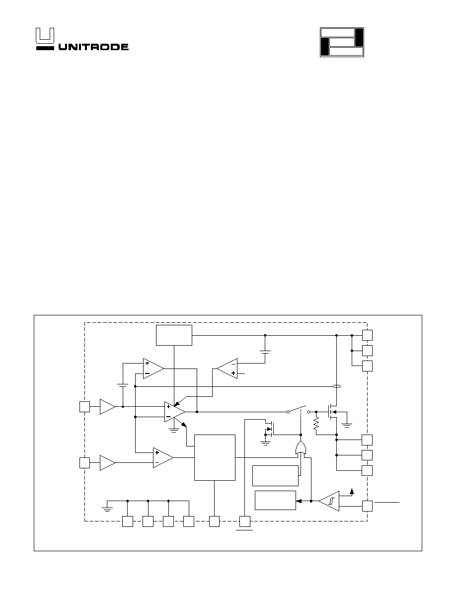
Low On Resistance Hot Swap Power Manager
9
8
5
4
13
12
10
6
7
3
2
1
INTERNAL
BIAS
THERMAL
SHUTDOWN
ON TIME
CONTROL
3% DUTY
CYCLE
CHARGE
PUMP
16
15
14
+
≠
VIN
VIN
VIN
VOUT
VOUT
VOUT
SHTDWN
FAULT
CT
HEAT SINK GND
PINS
GND
IFAULT
IMAX
CURRENT
FAULT LEVEL
OVERLOAD
COMPARATOR
OVERCURRENT
COMPARATOR
REVERSE
COMPARATOR
V
OUT
+
20mV
CURRENT SENSE
1.5V
H = OPEN
MAXIMUM
CURRENT
LEVEL
+
BLOCK DIAGRAM
UDG-99153
DESCRIPTION
The UCC3918 Low on Resistance Hot Swap Power Manager provides complete
power management, hot swap capability, and circuit breaker functions. The only
components needed to operate the device, other than supply bypassing, are a tim-
ing capacitor, and 2 programming resistors. All control and housekeeping functions
are integrated, and externally programmable. These include the fault current level,
maximum output sourcing current, maximum fault time, and startup delay. In the
event of a constant fault, the internal fixed 3% duty cycle ratio limits the average
output power. The IFAULT pin allows linear programming of the fault level current
from 0A to 4A.
Fast overload protection is accomplished by an additional overload comparator. Its
threshold is internally set above the maximum sourcing current limit setting. In the
event of a short circuit or extreme current condition, this comparator is tripped,
shutting down the output. This function is needed since the maximum sourcing cur-
rent limit loop has a finite bandwidth.
When the output current is below the fault level, the output MOSFET is switched on
with a nominal resistance of 0.06
. When the output current exceeds the fault level
or the maximum sourcing level, the output remains on, but the fault timer starts
charging CT. Once CT charges to a preset threshold, the switch is turned off, and
remains off for 30 times the programmed fault time. When the output current
reaches the maximum sourcing level, the MOSFET transitions form a switch to a
constant current source.
(continued)
application
INFO
available
2
UCC2918
UCC3918
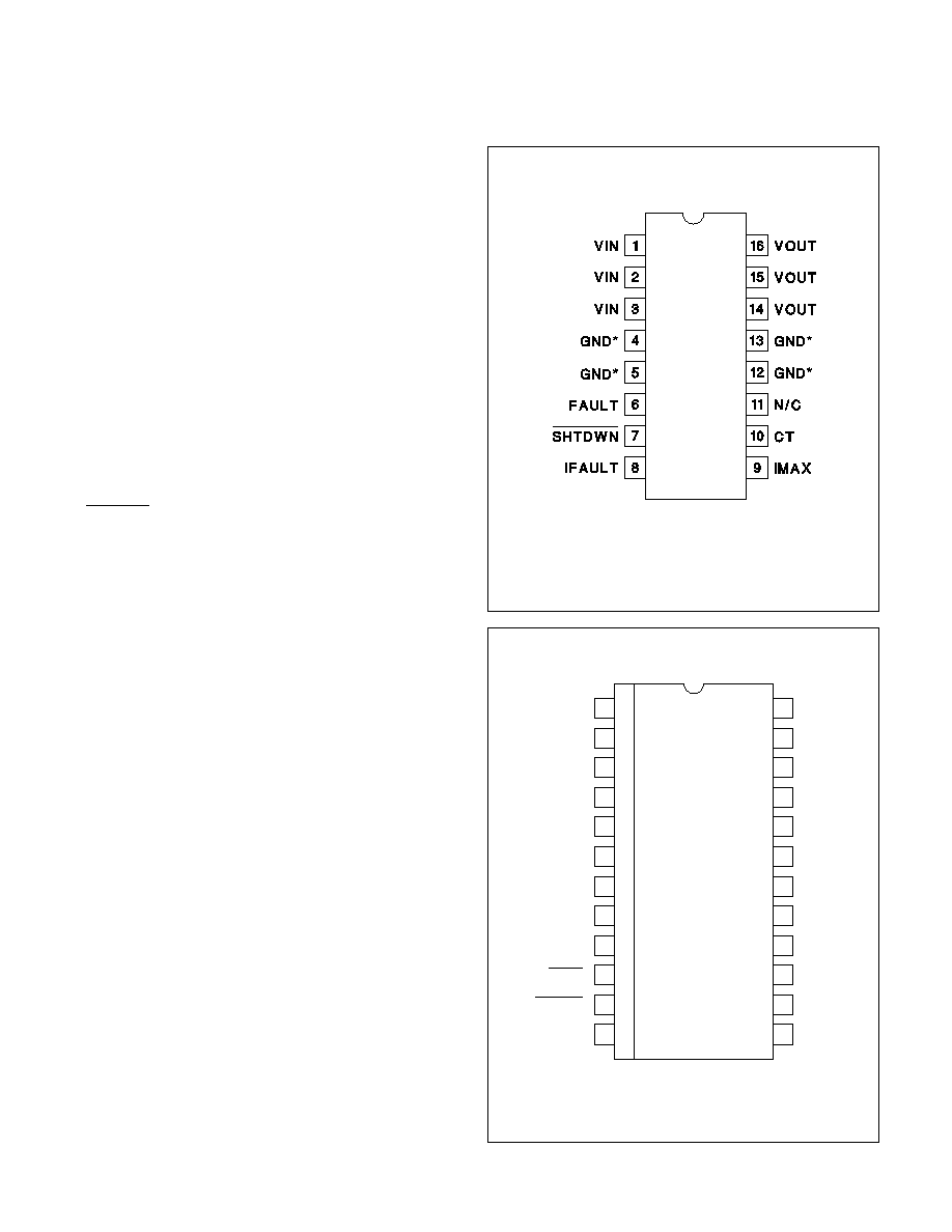
CONNECTION DIAGRAM
DIL-16, SOIC-16 (Top View)
N Package, DP Package
ABSOLUTE MAXIMUM RATINGS
Input Supply Voltage (VIN) . . . . . . . . . . . . . . . . . . . . . . . . . . 8V
SOIC Power Dissipation . . . . . . . . . . . . . . . . . . . . . . . . . . 2.5W
Fault Output Sink Current . . . . . . . . . . . . . . . . . . . . . . . . . 50mA
Fault Output Voltage . . . . . . . . . . . . . . . . . . . . . . . . . . . . . . VIN
Output Current (DC) . . . . . . . . . . . . . . . . . . . . Internally Limited
Input Voltage
SHTDWN, IFAULT, IMAX . . . . . . . . . . . . . . . . . ≠0.3V to VIN
Storage Temperature Range . . . . . . . . . . . . . ≠65∞C to +150∞C
Operating Junction Temperature Range . . . . ≠55∞C to +150∞C
Lead Temperature (Soldering, 10 sec.) . . . . . . . . . . . . . +300∞C
Unless otherwise indicated, voltages are reference to ground
and currents are positive into, negative out of the specified
terminal. Pulsed is defined as a less than 10% duty cycle with a
maximum duration of 500
µS. Consult Packaging Section of
Databook for thermal limitations and considerations of package.
DESCRIPTION (continued)
The UCC3918 is designed for unidirectional current flow,
emulating an ideal diode in series with the power switch.
This feature is particularly attractive in applications where
many devices are powering a common bus, such as with
SCSI Termpwr. The UCC3918 can also be put into the
sleep mode, drawing only 1
µA of supply current.
Other features include an open drain fault output indica-
tor, thermal shutdown, undervoltage lockout, 3V to 6V
operation, and a low thermal resistance small outline
power package.
* Pin 5 serves as the lowest impedance to the electrical
ground. Pins 4, 12, and 13 serve as heat sink/ground.
These pins should be connected to large etch PCB areas
to help dissipate heat. For N Package, pins 4, 12, and 13
are N/C.
SHTDWN
VOUT
VOUT
VOUT
N/C
GND*
GND*
GND*
VOUT
1
2
3
4
5
6
7
8
9
24
23
22
21
20
19
18
17
16
VIN
VIN
FAULT
GND*
GND*
VIN
GND*
GND*
VIN
10
11
12
GND*
IFAULT
IMAX
GND*
GND*
15
14
13
CT
TSSOP-24 (Top View)
PWP Package
* Pin 9 serves as the lowest impedance to the electrical
ground. Pins 5, 6, 7, 8, 16, 17, 18, 19 and 20 serve as heat
sink/ground.
3
UCC2918
UCC3918
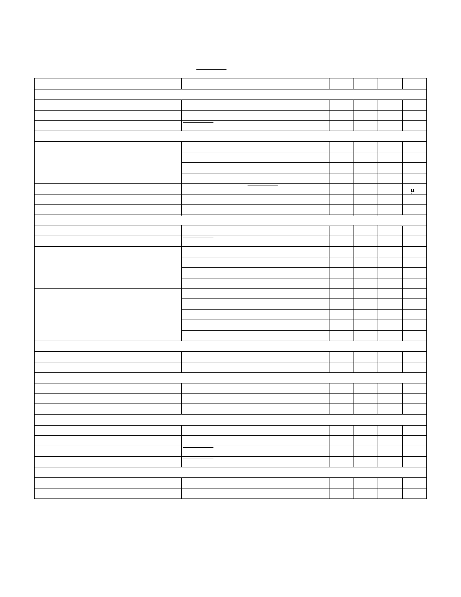
ELECTRICAL CHARACTERISTICS
: Unless otherwise specified, T
A
= 0∞C to 70∞C for the UCC3918, ≠40∞C to 85∞ for the
UCC2918, VIN = 5V. R
IMAX
= 42.2k, R
IFAULT
= 52.3k, SHTDWN = 2.4. T
A
= T
J
.
PARAMETER
TEST CONDITIONS
MIN
TYP
MAX
UNITS
Supply Section
Voltage Input Range, VIN
3
5
6
V
V
DD
Supply Current
No Load
1
2
mA
Sleep Mode Current
SHTDWN = 0.2V
0.5
5
µA
Output Section
RDS
ON
I
OUT
= 1A to 4A, VIN = 5V, TA = 25∞C
0.075
0.095
I
OUT
= 1A to 4A, VIN = 3V, TA = 25∞C
0.09
0.116
I
OUT
= 1A to 4A, VIN = 5V
0.75
0.125
I
OUT
= 1A to 4A, VIN = 3V
0.09
0.154
Reverse Leakage Current
V
IN
= 0V, V
OUT
= 5V, SHTDWN = 0V
20
A
Initial Startup Time
(Note 1)
100
µS
Thermal Shutdown
(Note 1)
170
DEG
Output Section (cont)
Thermal Hysteresis
(Note 1)
10
DEG
Output Leakage
SHTDWN = 0.2V
20
µA
Trip Current
R
IFAULT
= 105k
0.75
1
1.25
A
R
IFAULT
= 52.3k
1.7
2
2.3
A
R
IFAULT
= 34.8k
2.5
3
3.5
A
R
IFAULT
= 25.5k
3.3
4
4.7
A
Maximum Output Current
R
IMAX
= 118k
0.3
1
1.7
A
R
IMAX
= 60.4k
1
2
3
A
R
IMAX
= 42.2k
2
3
4
A
R
IMAX
= 33.2k
2.5
3.8
5.1
A
R
IMAX
= 27.4k
3.0
4.6
6.2
A
Fault Section
C
T
Charge Current
V
CT
= 1V
≠50
≠36
≠22
µA
C
T
Discharge Current
V
CT
= 1V
0.5
1.2
2.0
µA
Fault Section (cont.)
Output Duty Cycle
VOUT = 0V
1.5
3
6
%
C
T
Fault Threshold
0.8
1.3
1.8
V
C
T
Reset Threshold
0.25
0.5
0.75
V
Shutdown Section
Shutdown Threshold
1.1
1.5
2.0
V
Shutdown Hysteresis
100
mV
Input Low Current
SHTDWN = 0V
≠500
0
500
nA
Input High Current
SHTDWN = 2V
≠2
≠1
≠0.5
µA
Open Drain Fault Output
High Level Output Current
1
µA
Low Level Output Voltage
I
OUT
= 1mA
0.4
0.9
V
Note 1: Guaranteed by design. Not 100% tested in production.
4
UCC2918
UCC3918
PIN DESCRIPTIONS
CT: A capacitor connected to this pin sets the maximum
fault time. The maximum must be more than the time to
charge external load capacitance. The maximum fault
time is defined as
T
C
FAULT
T
=
∑
∑
27 8 10
3
.
Once the fault time is reached the output will shutdown
for a time given by
T
C
SD
T
=
∑
∑
0 833 10
6
.
,
this equates to a 3% duty cycle.
FAULT: Open drain output, which pulls low upon any
condition which causes the output to open; Fault, Ther-
mal Shutdown, Shutdown, and maximum sourcing cur-
rent greater than the fault time.
GND: This is the most negative voltage in the circuit. All
4 ground pins should be used, and properly heat sunk on
the PCB.
IFAULT: A resistor connected from this pin to ground
sets the fault threshold. The resistor vs fault current is
set by the formula
R
k
I
FAULT
TRIP
=
105
IMAX: A resistor connected from this pin to ground sets
the maximum sourcing current. The resistor vs the output
sourcing current is set by the formula,
R
k
Maximum Sourcing Current
FAULT
=
126
SHTDWN: When this pin is brought low, the IC is put into
sleep mode. The input threshold is hysteretic, allowing
the user to program a startup delay with an external RC
circuit.
VIN: This is the input voltage to the UCC3918. The rec-
ommended operating voltage range is 3V to 6V. All VIN
pins should be connected together and to the power
source.
VOUT: Output voltage for the circuit breaker. When
switched the output voltage will be approximately VIN ≠
0.06
∑ I
OUT
. All VOUT pins should be connected to-
gether and to the load.
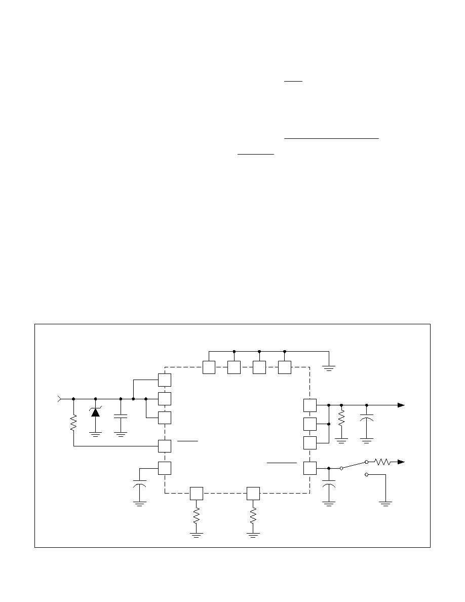
9
8
5
4
13
12
10
6
7
3
2
1
16
15
14
VIN
VIN
VIN
VOUT
VOUT
VOUT
SHTDWN
FAULT
CT
HEAT SINK GND
PINS
GND
IFAULT
IMAX
R
IMAX
R
IFAULT
C
T
C
SD
R
SD
V
IN
S6
R
L
C
OUT
V
OUT
C
IN
D1
R1
V
IN
Figure 1. Evaluation circuit.
APPLICATION INFORMATION
UDG-99152
5
UCC2918
UCC3918
Protecting The UCC3918 From Voltage Transients
The parasitic inductance associated with the power dis-
tribution can cause a voltage spike at V
IN
if the load
current is suddenly interrupted by the UCC3918.
It is
important to limit the peak of this spike to less than 6V
to prevent damage to the UCC3918
. This voltage spike
can be minimized by:
∑ Reducing the power distribution inductance (e.g.,
twist the positive "+" and negative "≠" leads of the
power supply feeding V
IN
, locate the power supply
close to the UCC3918 or use a PCB ground plane).
∑ Decoupling V
IN
with a capacitor, C
IN
(refer to Fig. 1),
located close to the V
IN
pin. This capacitor is typically
less than 1
µF to limit the inrush current.
∑ Clamping the voltage at V
IN
below 6V with a Zener
diode, D1 (refer to Fig. 1), located close to the V
IN
pin.
Estimating Maximum Load Capacitance
For circuit breaker applications, the rate at which the to-
tal output capacitance can be charged depends on the
maximum output current available and the nature of the
load. For a constant-current current-limited circuit
breaker, the output will come up if the load asks for less
than the maximum available short-circuit current.
To guarantee recovery of a duty-cycle of the cur-
rent-limited circuit breaker from a short-circuited load con-
dition, there is a maximum total output capacitance which
can be charged for a given unit ON time (Fault time). The
design value of ON or Fault time can be adjusted by
changing the timing capacitor C
T
.
For worst-case constant-current load of value just less
than the trip limit; C
OUT(max)
can be estimated from:
C
I
I
C
V
OUT
MAX
LOAD
T
OUT
(max)
(
≠
)
∑
∑
28 10
3
Where V
OUT
is the output voltage and I
MAX
is the maxi-
mum, sourcing current.
For a resistive load of value RI, the value of C
OUT(max)
can
be estimated from:
C
C
R
In
V
I
R
OUT
T
L
OUT
MAX
L
(max)
∑
∑
∑
-
∑
28 10
1
1
3
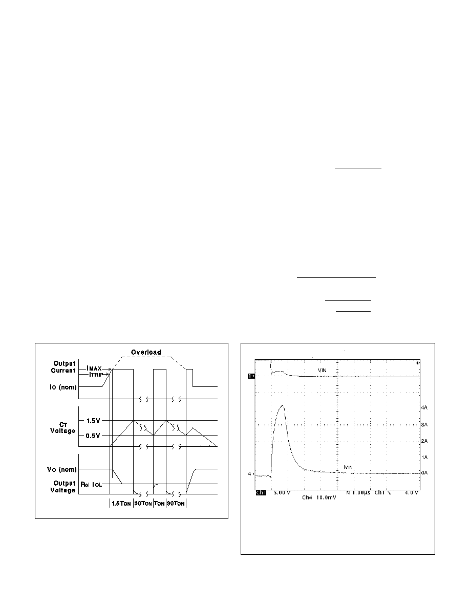
APPLICATION INFORMATION (cont.)
Figure 2. Load current, timing capacitor voltage and
output voltage of the UCC3918 under fault.
UDG-97071
Figure 3.
C
OUT
R
L
C
IN
R
IFAULT
R
IMAX
22
µ
F
5
5
µ
F
52.3k
42.0k
Input driven with a pulse generator, shows C
OUT
discharg-
ing through R
L
and conducting through UCC3918 FET in
the reverse direction.
6
UCC2918
UCC3918
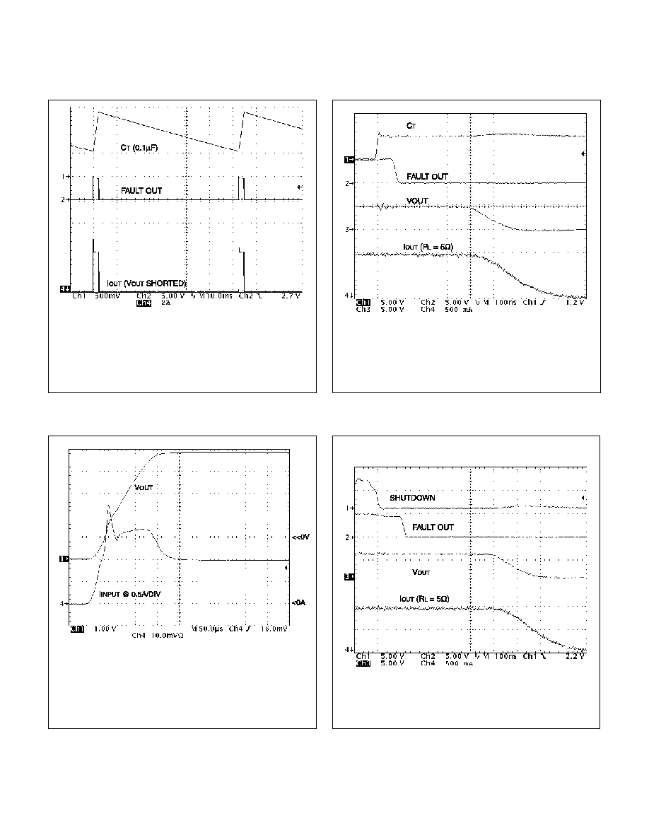
Figure 4. UCC3918 in shorted condition.
APPLICATION INFORMATION (cont.)
V
OUT
R
L
C
IN
R
IFAULT
R
IMAX
0V
SHORT
5
µ
F
52.3k
42.2k
Figure 5. Input hot swap.
C
OUT
R
L
C
IN
R
IFAULT
R
IMAX
22
µ
F
5
5
µ
F
52.3k
60.4k
Input switched on through external FET. V
OUT
shows I
MAX
linear amplifier limiting the changing current of C
OUT
.
Figure 6. C
T
to V
OUT
delay (fault condition).
C
OUT
R
L
C
IN
R
IFAULT
R
IMAX
C
T
0
µ
F
5
5
µ
F
52.3k
42.4k
OPEN
Figure 7. Shutdown delay to V
OUT
off.
C
OUT
R
L
C
IN
R
IFAULT
R
IMAX
0
µ
F
5
5
µ
F
52.3k
42.4k

7
UCC2918
UCC3918
Figure 8. Shutdown delay to V
OUT
on.
APPLICATION INFORMATION (cont.)
C
OUT
R
L
C
IN
R
IFAULT
R
IMAX
0
µ
F
5
5
µ
F
52.3k
42.4k
I
OUT
(A)
RDS
ON
mOh
m
s
Figure 9. RDS
ON
vs I
OUT
.
SAFETY RECOMMENDATIONS
Although the UCC3918 is designed to provide system
protection for all fault conditions, all integrated circuits
can ultimately fail short. For this reason, if the UCC3918
is intended for use in safety critical applications where
UL
©
or some other safety rating is required, a redundant
safety device such as a fuse should be placed in series
with the power device. The UCC3918 will prevent the
fuse from blowing for virtually all fault conditions, in-
creasing system reliability and reducing maintenance
cost, in addition to providing the hot swap benefits of the
device.
40
50
60
70
80
90
100
110
-60
-40
-20
0
20
40
60
80
100
120
TEMPERATURE (∞C)
RDS
ON
mOh
m
s
VIN = 5V, I = 1A
VIN = 3V, I = 1A
AVERAGE
VIN = 3V, I = 4A
VIN = 5V, I = 4A
Figure 10. RDS
ON
vs temperature.
UNITRODE CORPORATION
7 CONTINENTAL BLVD. ∑ MERRIMACK, NH 03054
TEL. (603) 424-2410 FAX (603) 424-3460