 | –≠–ª–µ–∫—Ç—Ä–æ–Ω–Ω—ã–π –∫–æ–º–ø–æ–Ω–µ–Ω—Ç: UCC29412 | –°–∫–∞—á–∞—Ç—å:  PDF PDF  ZIP ZIP |
UCC19411/2/3
UCC29411/2/3
UCC39411/2/3
PRELIMINARY
DESCRIPTION
The UCC39411 family of
low input voltage, single inductor boost
converters is optimized to operate from a single or dual alkaline cell, and
steps up to a 3.3V, 5V, or adjustable output at 200mW. The UCC39411
family also provides an auxiliary 7V output, primarily for the gate drive
supply, which can be used for applications requiring an auxiliary output,
such as 5V, by linear regulating. The primary output will start up under full
load at input voltages typically as low as 0.8V with a guaranteed max of
1V, and will operate down to 0.5V once the converter is operating,
maximizing battery utilization.
The
UCC39411
family
is
designed
to
accommodate
demanding
applications such as pagers and cell phones that require high efficiency
over a wide operating range of several milli-watts to a couple of hundred
milli-watts. High efficiency at low output current is achieved by optimizing
switching and conduction losses with a low total quiescent current (50
µA).
At higher output current the 0.5
switch, and 1.2 synchronous rectifier
along with continuous mode conduction provide high power efficiency. The
wide input voltage range of the UCC39411 family can accommodate other
power sources such as NiCd and NimH.
The 39411 family also provides shutdown control. Packages available are
the 8 pin SOIC (D), 8 pin DIP (N or J), and 8 pin TSSOP (PW) to optimize
board space.
Low Power Synchronous Boost Converter
FEATURES
∑ 1V Input Voltage Operation Start-up
Guaranteed under FULL Load on
Main Output, and Operation Down to
0.5V
∑ 200mW Output Power at Battery
Voltages as low as 0.8V
∑ Secondary 7V Supply from a Single
Inductor
∑ Output Fully Disconnected in
Shutdown
∑ Adaptive Current Mode Control for
Optimum Efficiency
∑ High Efficiency over Wide Operating
Range
∑ 6µA Shutdown Supply Current
∑ Output Reset Function with
Programmable Reset Period
SLUS245A - MARCH 1999
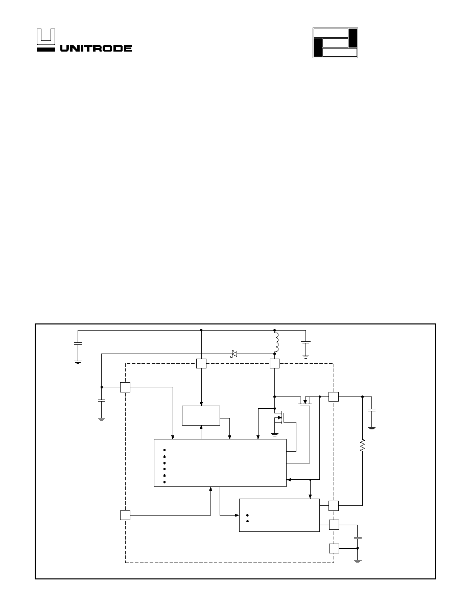
1
4
7
6
VOUT
GND
3.3V 200mW
5
C
T
R
RES
3
100
µF
RESET CONTROL CIRCUIT
GLITCH SUPRESSION
PROGRAMMABLE TIMING
MODULATOR CONTROL CIRCUIT
SYNCHRONOUS RECTIFICATION CIRCUITRY
ANTI-CROSS CONDUCTION
START-UP
MULTIPLEXING LOGIC
MAX INPUT POWER CONTROL
ADAPTIVE CURRENT CONTROL
START-UP
CIRCUITRY
1.2
CT
RESB
2
SD/FB
100
µF
VIN
SW
8
VGD
0.5
100
µF
1V TO 3.5V
22
µH
+
SIMPIFIED BLOCK DIAGRAM AND APPLICATION CIRCUIT (UCC39412)
UDG-98067
Note: Pinout shown is for the TSSOP Package. Consult Package Descriptions for DIP and SOIC configurations.
application
INFO
available
2
UCC19411/2/3
UCC29411/2/3
UCC39411/2/3
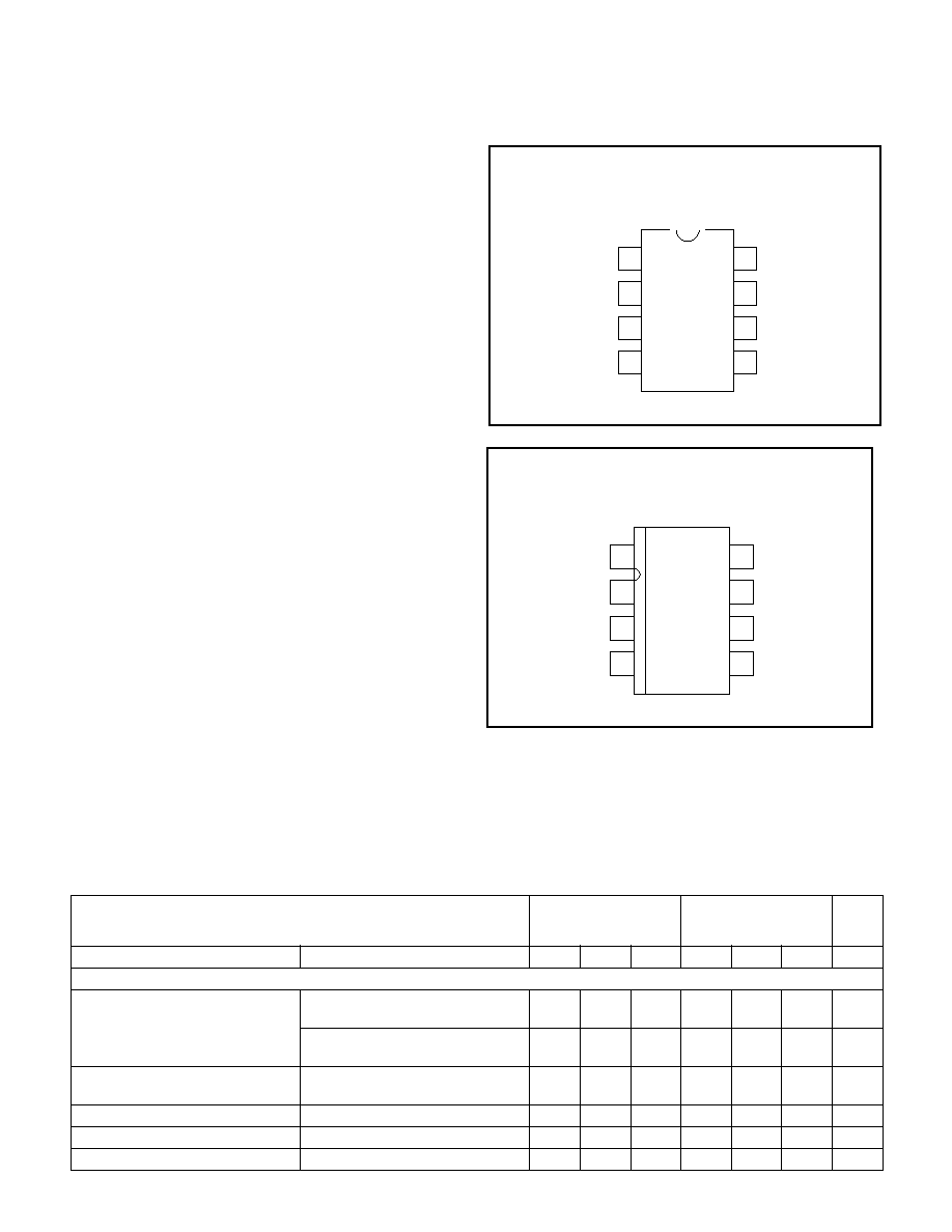
DIL-8, SOIC-8 (TOP VIEW)
N or J Package, D Package
ABSOLUTE MAXIMUM RATINGS
VIN Voltage . . . . . . . . . . . . . . . . . . . . . . . . . . . . . . ≠0.3V to 10V
SD Voltage . . . . . . . . . . . . . . . . . . . . . . . . . . . . . . . ≠0.3V to V
IN
VGD Voltage . . . . . . . . . . . . . . . . . . . . . . . . . . . . ≠0.3V to 14V
SW Voltage . . . . . . . . . . . . . . . . . . . . . . . . . . . . . . ≠0.3V to 15V
Currents are positive into, negative out of the specific terminal.
Consult Packaging Section of the Databook for thermal limita-
tions and considerations of packages.
CT
GND
SW
RESB
1
2
3
4
8
7
6
5
VGD
VOUT
VIN
SD/FB
CONNECTION DIAGRAMS
ELECTRICAL CHARACTERISTICS:
T
J
= 0∞C to +70∞C for the UCC39411/2/3, T
J
= ≠40∞C to +85∞C for the
UCC29411/2/3, T
J
= ≠55C to +125∞C for the UCC19411/2/3, V
IN
= 1.25V for UCC39411/2, V
IN
= 2.5V for the UCC39413, T
A
=T
J
.
UCC39411
UCC39412
UCC39413
UCC19411/2/3
UCC29411/2/3
PARAMETER
TEST CONDITIONS
MIN
TYP
MAX
MIN
TYP
MAX
UNITS
VIN Section
Minimum Start-up Voltage
No External VGD Load, T
J
=25∞C,
I
OUT
=60mA (Note 1)
0.8
1
.08
1
V
No External VGD Load, I
OUT
=60mA
(Note 1)
0.9
1.1
1.2
1.4
V
Minimum Dropout Voltage
No External VGD Load, I
OUT
=10mA
(Note 1)
0.5
0.7
V
Input Voltage Range
1.1
3.2
1.3
3.2
V
Quiescent Supply Current
(Note 2)
6
12
8
16
µ
A
Supply Current at Shutdown
SD = GND
6
12
8
16
µ
A
SW
VOUT
VGD
GND
1
2
3
4
8
7
6
5
SD/FB
VIN
RESB
CT
TSSOP-8 (TOP VIEW)
PW Package

3
UCC19411/2/3
UCC29411/2/3
UCC39411/2/3
ELECTRICAL CHARACTERISTICS:
T
J
= 0∞C to +70∞C for the UCC39411/2/3, T
J
= ≠40∞C to +85∞C for the
UCC29411/2/3, T
J
= ≠55C to +125∞C for the UCC19411/2/3, V
IN
= 1.25V for UCC39411/2, V
IN
= 2.5V for the UCC39413, T
A
=T
J
.
UCC39411
UCC39412
UCC39413
UCC19411/2/3
UCC29411/2/3
PARAMETER
TEST CONDITIONS
MIN
TYP
MAX
MIN
TYP
MAX
UNITS
Output Section
Quiescent Supply Current
(Note 2)
15
28
20
37
µ
A
Supply Current at Shutdown
SD = GND
3
6
5
10
µ
A
Regulation Voltage (UCC39412) 1V < V
IN
< 3V
3.2
3.3
3.39
3.15
3.3
3.45
V
1V < V
IN
< 3V, 0mA<I
OUT
<60mA
(Note 1)
3.17
3.3
3.43
3.11
3.3
3.5
V
Regulation Voltage (UCC39413) 1V < V
IN
< 5V
4.85
5
5.15
4.78
5
5.23
V
1V < V
IN
< 5V, 0mA<I
OUT
<60mA
(Note 1)
4.8
5
5.2
4.71
5
5.3
V
ADJ Voltage (UCC39411)
1V < V
IN
< 3V
1.212
1.25
1.288
1.194
1.25
1.306
V
VGD Output Section
Quiescent Supply Current
(Note 2)
20
40
27
55
µ
A
Supply Current at Shutdown
SD = GND
20
40
27
55
µ
A
Regulation Voltage
(UCC39411/2)
1V < V
IN
< 3V
6.3
7
7.7
6.3
7
7.7
V
1V < V
IN
< 3V, 0mA<I
OUT
<10mA
(Note 1)
6.3
7
7.7
6.3
7
7.7
V
Regulation Voltage (UCC39413) 1V < V
IN
< 5V
7.7
8.5
9.3
7.7
8.5
9.3
V
1V < V
IN
< 5V, 0mA<I
OUT
<10mA
(Note 1)
7.7
8.5
9.3
7.7
8.5
9.3
V
Inductor Charging Section (L=22
µ
H)
Peak Discontinuous Current
Operating Range, L=22.1
µH
180
250
300
180
250
300
mA
Peak Continuous Current
385
550
715
385
550
715
mA
Charge Switch RDS
ON
D Package
0.5
0.75
0.6
0.85
Current Limit Delay
(Note 1)
50
50
ns
Synchronous Rectifier Section
Rectifier RDS
ON
D Package
1.2
1.8
1.4
2.16
Shutdown Section
Threshold
0.4
0.6
0.8
0.2
0.6
0.9
V
Input Bias Current
SD = GND
2
5
15
2
5
15
µ
A
SD = 1.25V
5
20
20
100
nA
Reset Section
Threshold (UCC39411)
1.08
1.125
1.17
1.07
1.125
1.18
V
Threshold (UCC39412)
2.85
2.97
3.09
2.83
2.97
3.11
V
Threshold (UCC39413)
4.32
4.5
4.68
4.3
4.5
4.7
V
Reset Period
C
T
= 0.15
µ
F
113
188
263
94
188
282
ms
V
OUT
to Reset Delay
V
OUT
Falling at ≠1mV/
µ
s (Note 1)
60
60
µ
s
Sink Current
1
20
1
20
mA
Output Low Voltage
I
OUT
= 500
µ
A
0.1
0.1
V
Output Leakage
0.5
0.5
µ
A
Note 1 : Guaranteed by design and alternate test methods. Not 100% tested in production.
Note 2: For the UCC39411 FB=1.306V, VGD=7.7V, For the UCC39412 V
OUT
=3.5V and VGD=7.7V, For the UCC39413
V
OUT
=5.3V, VGD=9.3V.

4
UCC19411/2/3
UCC29411/2/3
UCC39411/2/3
PIN DESCRIPTIONS
VIN: Input Voltage to supply the IC during start-up. After
the output is running the IC draws power from VOUT or
VGD.
SW: An inductor is connected between this node and
VIN. The VGD (Gate Drive Supply) flyback diode is also
connected to this pin. When servicing the main output
supply this pin will pull low charging the inductor, then
shut off dumping the energy through the synchronous
rectifier to the output. When servicing the VGD supply
the internal synchronous rectifier stays off and the en-
ergy is diverted to VGD through the flyback diode. During
discontinuous portions of the inductor current, a MOS-
FET resistively connects VIN to SW damping excess cir-
culating energy to eliminate undesired high frequency
ringing.
VGD: The VGD pin which is coarsely regulated around
7V (8.5V for the UCC39413) is primarily used for the
gate drive supply for the power switches in the IC. This
pin can be loaded with up to 10mA as long as it does not
present a load at voltages below 2V (this ensures proper
start-up of the IC). The VGD supply can go as low as
6.3V without interfering with the servicing of the main
output. Below 6.3V, VGD will have the highest priority.
VOUT: Main output voltage (3.3V, 5V, or adjustable)
which has highest priority in the multiplexing scheme, as
long as VGD is above the critical level of 6.3V. Startup at
full load is achievable at input voltages down to 1V.
CT: This pin provides the timer for determining the reset
period. The period is controlled by placing a capacitor to
ground of value C = (0.81e
-6
)
∑T where T is the desired
reset period.
RESB: This pin provides an active low signal to alert the
user when the main output voltage falls below 10% of its
targeted value. The open drain output can be used to re-
set a microcontroller which may be powered off of the
main output voltage.
SD/FB: For the UCC39411, this pin is used to adjust the
output voltage via a resistive divider from VOUT. It also
serves as the shutdown pin for all three versions. Pulling
this pin low provides a shutdown signal to the IC.
GND: Ground of the IC.
APPLICATION INFORMATION
Operation
A detailed block diagram of the UCC39411 is shown in
Figure 1. Unique control circuitry provides high efficiency
power conversion for both light and heavy loads by tran-
sitioning between discontinuous and continuous conduc-
tion based on load conditions.
Figure 2 depicts
converter waveforms for the application circuit shown in
Figure 3.
A single 22
µH inductor provides the energy
pulses required for a highly efficient 3.3V converter at up
to 200mW output power
At time t1 the 3.3V output voltage has dropped below its
lower threshold, and the inductor is charged with an on
time determined by: T
ON
= 5.5
µs/VIN. For a 1.25V input
and a 22
µH inductor, the resulting peak current is ap-
proximately 250mA. At time t2, the inductor begins to
discharge with a minimum off time of approximately 1
µs.
Under lightly loaded conditions, the amount of energy
delivered in this single pulse would satisfy the voltage
control loop, and the converter would not command any
more energy pulses until the output again drops below
the lower voltage threshold
At time t3 the VGD supply drops below its lower thresh-
old, but the output voltage is still above its threshold
point. This results in an energy pulse to the gate drive
supply at t4. In some cases, a single pulse supplied to
VGD is insufficient to raise the VGD voltage level enough
to satisfy the voltage loop. Under this condition, multiple
pulses will be supplied to VGD.
Note: when the
UCC39411/2/3 is servicing VGD only, the IC will maintain
a discontinuous mode of operation.
After time t4, the
3.3V output drops below its threshold and requests to be
serviced once the VGD cycle has completed, which oc-
curs at time t5.
Time t6 represents a transition between light load and
heavy load.
A single energy pulse is not sufficient to
force the output voltage above its upper threshold before
the minimum off time has expired and a second charge
cycle is commanded.
Since the inductor current does
not reach zero in this case, the peak current is greater
than 250mA at the end of the next charge on time. The
result is a ratcheting of inductor current until either the
output voltage is satisfied, or the converter reaches its
set current limit. At time t7, the gate drive voltage has
dropped below its 7V threshold but the converter contin-
ues to service the output because it has higher priority
unless VGD drops below
6.3V
Between time t7 and t8, the converter reaches its peak
current limit.
Once the peak current is reached, the converter oper-
ates in continuous mode with approximately 60mA of in-
5
UCC19411/2/3
UCC29411/2/3
UCC39411/2/3
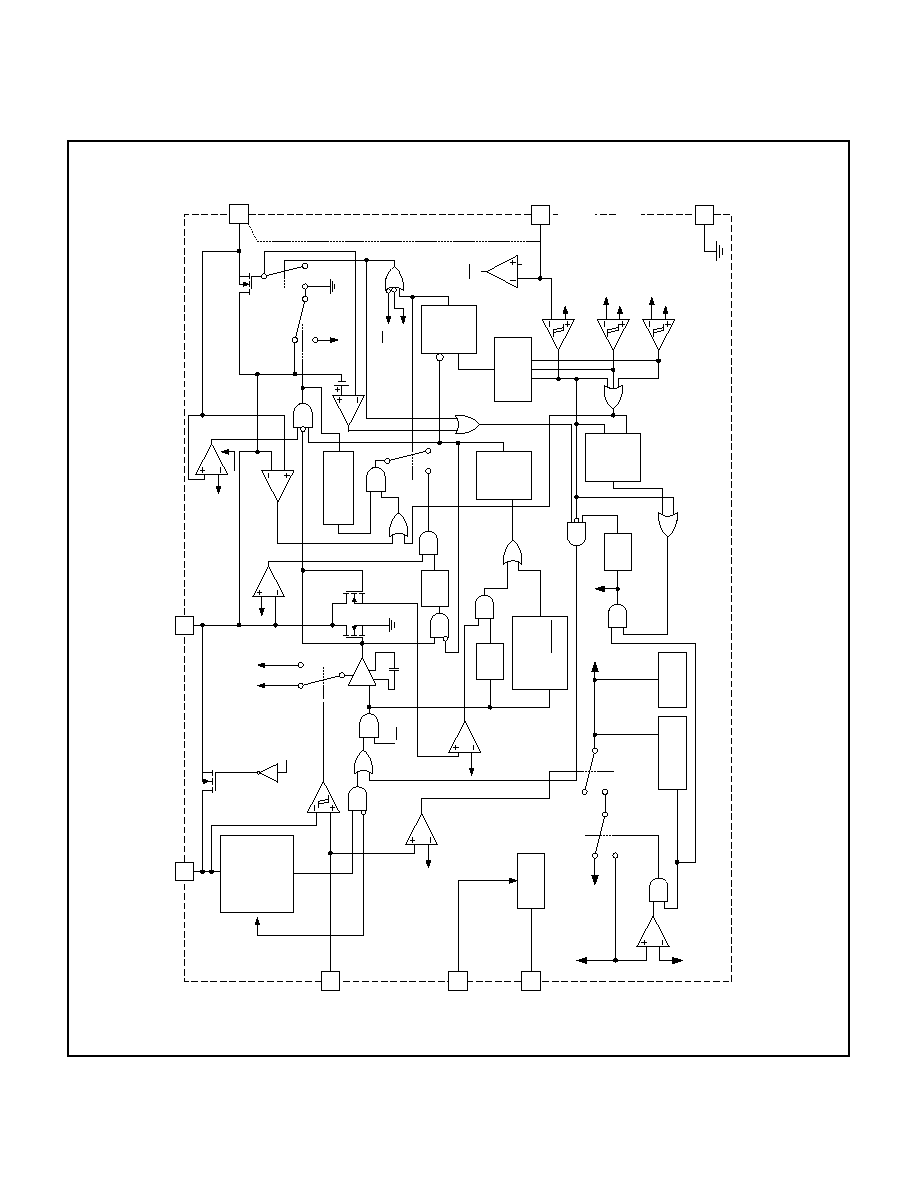
1
3
VG
D
SD
/
F
B
VO
U
T
0.
5V
VG
D
8
R
ESET
4
5
2
200k
HZ
ST
AR
T
-
U
P
O
S
CI
LLA
T
O
R
AN
D
CO
NT
RO
L
VL
O
W
SW
1.
25V
(
UCC39411)
3.
3V
(
UCC39412)
5.
0V
(
UCC39413)
PR
I
O
R
I
T
Y
E
NCO
DE
R
VG
D
7.
5V
(
UCC39411/
2)
8.
5V
(
UCC39413)
VG
D
6V
(
UCC39411/
2)
7.
5V
(
UCC39413)
SD
CLK
D
Q
FR
O
M
S
D
V
R
E
F
GOOD
1
µ
S
R
IS
IN
G
ED
G
E
D
E
L
A
Y
R
S
D
Q
R
S
D
Q
1
µ
S
R.
E
.
D.
VO
N
I
N
T
E
RNA
L
BI
AS
1.
25
RE
F
E
RE
NCE
2.
5V
VG
D
VD
D
R
ESET
TIM
E
R
CT
6
CT
5V
GS
VR
EF
GOOD
FR
O
M
S
D
RI
S
I
NG
E
D
G
E
DE
LA
Y
T
ON
=5
.
5
E
-6
VBAT
50nS
R.
E
.
D.
0.
66A
MAX
C
PU
M
P
VBAT
T
OF
F
TIM
E
R
50nS
R.
E
.
D.
VO
N
VI
N
VBAT
VG
D
VG
D
1.
2
VO
U
T
7
Figure 1. Low power synchronous boost.
Notes: Switches are shown in the low state.
Pinout as shown is for the 8 pin D, N or J. See Package Descriptions for 8 pin SOIC.
APPLICATION INFORMATION (continued)
UDG-98068
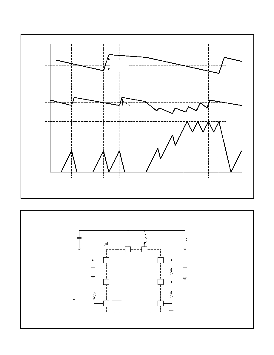
6
UCC19411/2/3
UCC29411/2/3
UCC39411/2/3
3
4
1
8
GND
L=10
µH TO
100
µH
7
R1
100
µF
6
SD/FB
10
µF
VIN
SW
2
VGD
10
µF
1-2 CELL ALKALINE
1.0V TO 3.2V
5
80nF
100k
V
OUT
CT
RESET
R2
VOUT
Note:
Shown pinout is for the TSSOP package. See Package Descriptions for DIP and SOIC pinouts.
Figure 3. Low power synchronous boost converter ADJ version ≠200mW.
VGD
RIPPLE
50mV/DIV
7V
t1
t2
t3
t4
t5
t6
t7
t8
t9
INDUCTOR
CURRENT
CURRENT
LIMIT
OUTPUT
RIPPLE
20mV/DIV
3.3V
HIGH LOAD CURRENT
LIGHT LOAD CURRENT
80mV P≠P
TYPICAL
20mV P≠P
TYPICAL
Figure 2. Inductor current and output ripple waveforms.
APPLICATION INFORMATION (continued)
UDG-98069
UDG-98070

7
UCC19411/2/3
UCC29411/2/3
UCC39411/2/3
ductor current ripple. At time t8, the 3.3V output is
satisfied and the converter can service the gate drive
voltage, VGD, which occurs at time t9
Shutdown Control
Shutdown of the UCC39411/2/3 is controlled via inter-
face with the SD/FB pin. Pulling the SD/FB pin low, for
all versions, causes the IC to go into shutdown. In the
UCC39412/3, the SD/FB pin is used solely as a shut-
down function. Therefore, the SD/FB pin for the
UCC39412 and UCC39413 can be directly controlled us-
ing conventional CMOS or TTL technology.
For the
UCC39411, interface into the SD/FB is slightly more
complicated due to the added feedback function. When
feeding back the output voltage to the SD/FB pin on the
UCC39411, the IC requires a thevenin impedance of at
least 200k
(500k for industrial/military applications) to
ground. Then, to accomplish shutdown of the IC, an
open drain device may be used.
Component Selection Inductor Selection
An inductor value of 22
µH will work well in most applica-
tions, but values between 10
µH to 100µH are also ac-
ceptable. Lower value inductors typically offer lower ESR
and smaller physical size. Due to the nature of the
"bang-bang" controllers, larger inductor values will typi-
cally result in larger overall voltage ripple, because once
the output voltage level is satisfied the converter goes
discontinuous, resulting in the residual energy of the in-
ductor causing overshoot.
It is recommended to keep the ESR of the inductor below
0.15
for 200mW applications. A Coilcraft DT3316P-223
surface mount inductor is one choice since it has a cur-
rent rating of 1.5A and an ESR of 84m
.
Other choices for surface mount inductors are shown in
Table 1.
Output Capacitor Selection
Once the inductor value is selected the capacitor value
will determine the ripple of the converter. The worst case
peak to peak ripple of a cycle is determined by two com-
ponents, one is due to the charge storage characteristic,
and the other is the ESR of the capacitor. The worst
case ripple occurs when the inductor is operating at max
current and is expressed as follows:
( )
(
)
V
I
L
C V
V
I
C
CL
O
I
CL
ESR
=
-
+
2
2
∑ I
CL
= the peak inductor current = 550mA
∑ V= Output ripple
∑ V
O
= Output Voltage
∑ V
I
= Input Voltage
∑ C
ESR
= ESR of the output capacitor.
A Sanyo OS-CON series surface mount capacitor
(10SN100M) is one recommendation. This part has an
ESR rating of 90m
at 100µF .
Other potential capacitor sources are shown in Table 2.
Input Capacitor Selection
Since the UCC39411 family does not require a large de-
coupling capacitor on the input voltage to operate prop-
erly, a 10
µF cap is sufficient for most applications.
Optimum efficiency will occur when the capacitor value is
large enough to decouple the source impedance, this
usually occurs for capacitor values in excess of 100
µF.
APPLICATION INFORMATION (continued)
MANUFACTURER
PART NUMBER
Sanyo Video
Components
OS-CON Series
San Diego, California
Tel: 619-661-6322
Fax: 619-661-1055
AVX
TPS Series
Sanford, Maine
Tel: 207-282-5111
Fax: 207-283-1941
Sprague
695D Series
Concord, New Hampshire
Tel: 603-224-1961
Table 2. Capacitor Suppliers
MANUFACTURER
PART NUMBERS
Coilcraft
DT Series
Cary, Illinois
Tel: 708-639-2361
Fax: 708-639-1469
Coiltronics
CTX Series
Boca Raton, Florida
Tel: 407-241-7876
Table 1. Inductor Suppliers
8
UCC19411/2/3
UCC29411/2/3
UCC39411/2/3
UNITRODE CORPORATION
7 CONTINENTAL BLVD. ∑ MERRIMACK, NH 03054
TEL. (603) 424-2410 ∑ FAX (603) 424-3460
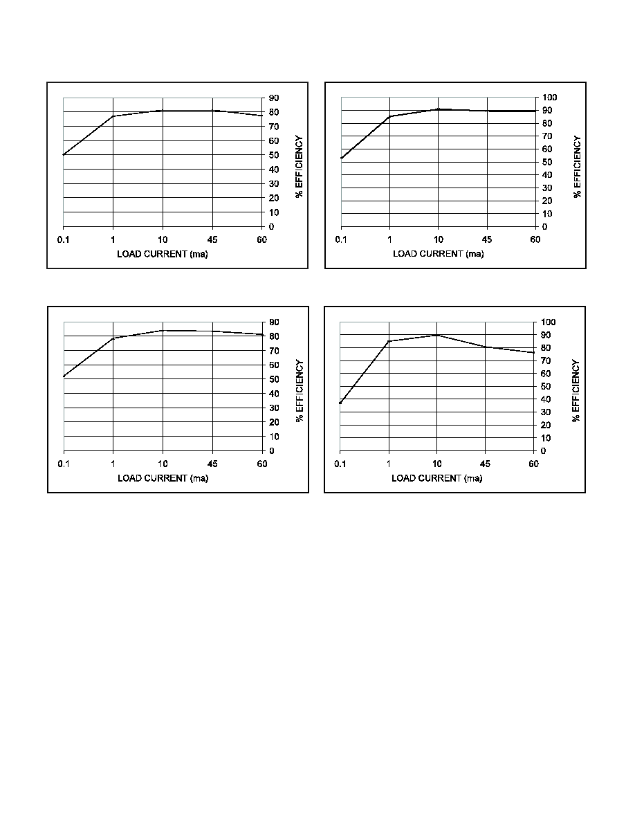
TYPICAL CHARACTERISTICS
Figure 4. Percent Efficiency at V
IN
= 1.0, V
OUT
= 3.3V
Figure 6. Percent Efficiency at V
IN
= 2.5, V
OUT
= 3.3V
Figure 5. Percent Efficiency at V
IN
= 1.25, V
OUT
= 3.3V
Figure 7. Percent Efficiency at V
IN
= 3.3, V
OUT
= 3.3V