 | –≠–ª–µ–∫—Ç—Ä–æ–Ω–Ω—ã–π –∫–æ–º–ø–æ–Ω–µ–Ω—Ç: UCC2941-5 | –°–∫–∞—á–∞—Ç—å:  PDF PDF  ZIP ZIP |

UCC2941-3/-5/-ADJ
UCC3941-3/-5/-ADJ
SLUS242 - JULY 1999
FEATURES
∑
1V Input Voltage Operation Startup
Guaranteed Under Full Load on Main
Output With Operation Down to 0.4V
∑
Input Voltage Range of 1V to V
OUT
+
0.5V
∑
500mW Output Power at Battery
Voltages as Low as 0.8V
∑
Secondary 9V Supply From a Single
Inductor
∑
Adjustable Output Power Limit Control
∑
Output Fully Disconnected in
Shutdown
∑
Adaptive Current Mode Control for
Optimum Efficiency
∑
8
µ
A Shutdown Supply Current
1V Synchronous Boost Converter
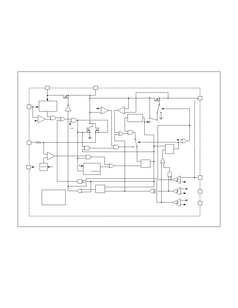
MODULATOR CONTROL CIRCUIT
SYNCHRONOUS RECTIFICATION CIRCUITRY
ANTI-CROSS CONDUCTION
STARTUP
MULTIPLEXING LOGIC
MAXIMUM INPUT POWER CONTROL
ADAPTIVE CURRENT CONTROL
4
5
6
7
1
8
3
2
+
≠
1.25V
UCC3941-ADJ
OPEN=SD
SD
10
µ
F
VGD
8V
STARTUP
CIRCUITRY
VIN
SW
+
10
µ
F
22
µ
H
0.8V TO VOUT +0.5V
100
µ
F
0.4
VOUT
PGND
*SGND/FB
PLIM
0.25
UCC3941-3 = 3.3V
UCC3941-5 = 5.0V
UCC3941-ADJ = 1.30V TO 6V
*FOR UCC3941-ADJ ONLY:
PIN 7 = SGND & PGND, PIN 6 = OUTPUT SENSE FEEDBACK, FB.
F
O
R
UCC3941-
ADJ
O
NL
Y
SIMPLIFIED BLOCK DIAGRAM AND APPLICATION CIRCUIT
UDG-98147
DESCRIPTION
The UCC3941 family of low input voltage single inductor boost converters
are optimized to operate from a single or dual alkaline cell, and step up to
a 3.3V, 5V, or an adjustable output at 500mW. The UCC3941 family also
provides an auxiliary 9V 100mW output, primarily for the gate drive supply,
which can be used for applications requiring an auxiliary output such as a
5V supply by linear regulating. The primary output will start up under full
load at input voltages typically as low as 0.8V, with a guaranteed maximum
of 1V, and will operate down to 0.4V once the converter is operating, maxi-
mizing battery utilization.
Demanding applications such as Pagers and PDA's require high efficiency
from several milli-watts to several hundred milli-watts, and the UCC3941
family accommodates these applications with >80% typical efficiencies
over the wide range of operation. The high efficiency at low output current
is achieved by optimizing switching and conduction losses along with low
quiescent current. At higher output current the 0.25
switch, and 0.4
syn-
chronous rectifier, along with continuous mode conduction, provide high ef-
ficiency. The wide input voltage range on the UCC3941 family can
accommodate other power sources such as NiCd and NiMH.
Other features include maximum power control and shutdown control.
Packages available are the 8-pin SOIC (D) and 8-pin DIP (N or J).
application
INFO
available
2
UCC2941-3/-5/-ADJ
UCC3941-3/-5/-ADJ
ELECTRICAL CHARACTERISTICS:
Unless otherwise specified, for UCC3941, T
A
= 0∞C to 70∞C; for UCC2941, T
A
= ≠40∞C
to 85∞C; VIN = 1.25V, T
A
= T
J
.
PARAMETER
TEST CONDITIONS
MIN
TYP
MAX
UNITS
VIN Section
Minimum Startup Voltage
No External VGD Load, T
J
= 25∞C, I
OUT
= 100mA (Note 1)
0.8
1.0
V
Minimum Start Voltage
No External VGD Load, I
OUT
= 100mA, T
J
= 0
∞
C to 85
∞
C
(Note 1)
0.9
1.1
V
Minimum Startup Voltage
No External VGD Load, T
J
= ≠40∞C to 0
∞
C
0.9
1.5
V
Minimum Dropout Voltage
No External VGD Load, I
OUT
= 100mA, VGD = 6.3V
(Note 1)
0.5
V
Input Voltage Range
1
VOUT
+0.5
V
Quiescent Supply Current
(Note 2)
13
25
µ
A
Supply Current at Shutdown
SD = Open
8
20
µ
A
Output Section
Quiescent Supply Current
(Note 2)
32
80
µ
A
Supply Current at Shutdown
SD = Open
6
15
µ
A
Regulation Voltage (UCC3941-3)
1V < VIN < 3V
3.18
3.25
3.37
V
1V < VIN < 3V, 0mA < I
OUT
< 150mA (Note 1)
3.17
3.30
3.43
V
Regulation Voltage (UCC3941-5)
1V < VIN < 5V
4.85
5.00
5.15
V
1V < VIN < 5V, 0mA < I
OUT
100mA (Note 1)
4.8
5.0
5.2
V
FB Voltage (UCC3941-ADJ)
1V < VIN < 3V
1.212
1.250
1.288
V
VGD Output Section
Quiescent Supply Current
(Note 2)
25
60
µ
A
Supply Current at Shutdown
SD = Open
8
20
µ
A
Regulation Voltage
1V < VIN < 3V
7.5
8.7
9.2
V
1V < VIN < 3V, 0mA < I
OUT
< 10mA (Note 1)
7.4
8.7
9.3
V
Inductor Charging Section (L = 22
µ
H)
Peak Discontinuous Current
Over Operating Range
0.50
0.85
A
Peak Continuous Current
R
PLIM
= 6.2
, UCC3941-3 and UCC3941-5
0.5
0.8
1.1
A
UCC3941-ADJ
0.6
0.9
1.3
A
ABSOLUTE MAXIMUM RATINGS
VIN Voltage . . . . . . . . . . . . . . . . . . . . . . . . . . . . . . ≠0.3V to 10V
SD Voltage . . . . . . . . . . . . . . . . . . . . . . . . . . . . . . ≠0.3V to VIN
PLIM Voltage. . . . . . . . . . . . . . . . . . . . . . . . . . . . . ≠0.3V to 10V
VGD Voltage . . . . . . . . . . . . . . . . . . . . . . . . . . . . . ≠0.3V to 15V
SW Voltage . . . . . . . . . . . . . . . . . . . . . . . . . . . . . . ≠0.3V to 15V
VOUT Voltage . . . . . . . . . . . . . . . . . . . . . . . . . . . . ≠0.3V to 10V
Storage Temperature . . . . . . . . . . . . . . . . . . . ≠65∞C to +150∞C
Junction Temperature . . . . . . . . . . . . . . . . . . . ≠55∞C to +150∞C
Lead Temperature (Soldering, 10 sec.) . . . . . . . . . . . . . +300∞C
Currents are positive into, negative out of the specified terminal.
Consult Packaging Section of Databook for thermal limitations
and considerations of packages.
Pin 6 is FB for UCC3941-ADJ.
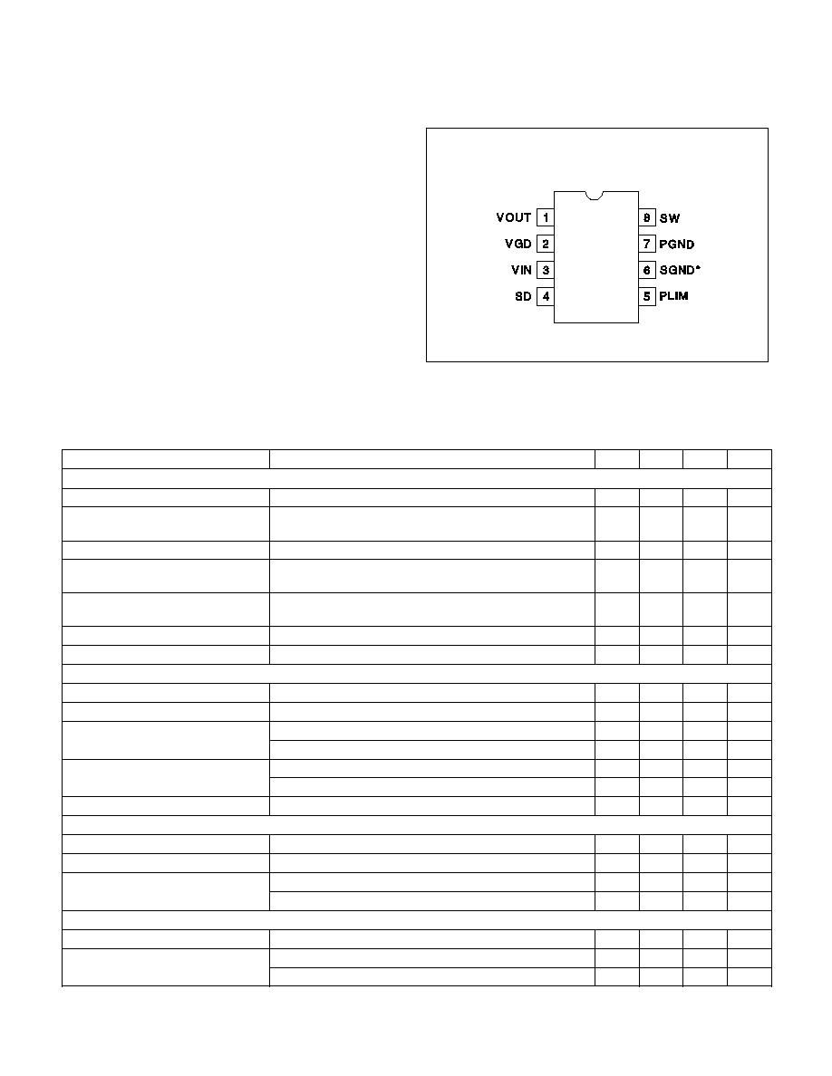
CONNECTION DIAGRAM
DIL-8, SOIC-8 (Top View)
N or J Package, D Package

3
UCC2941-3/-5/-ADJ
UCC3941-3/-5/-ADJ
ELECTRICAL CHARACTERISTICS:
Unless otherwise specified, for UCC3941, T
A
= 0∞C to 70∞C; for UCC2941, T
A
= ≠40∞C
to 85∞C; VIN = 1.25V, T
A
= T
J
.
PARAMETER
TEST CONDITIONS
MIN
TYP
MAX
UNITS
Inductor Charging Section
Charge Switch R
DS(on)
N and D Package, I = 200mA
0.25
0.4
Current Limit Delay
(Note 1)
50
ns
Synchronous Rectifier Section
Rectifier R
DS(on)
N and D Package, I = 200mA, UCC3941-ADJ V
OUT
= 3.3V
and UCC3941≠3
0.35
0.6
N and D Package, I = 200mA, UCC3941-5
0.5
0.8
Shutdown Section
Shutdown Bias Current
≠10
≠7
µ
A
Note 1: Performance from application circuit shown in Figures 3 - 5 guaranteed by design and alternate testing methods, but not
100% tested as shown in production.
Note 2: For the UCC3941-3, VOUT = 3.47V and VGD = 9.3V. For the UCC3941-5, VOUT = 5.25V, VGD = 9.3V. For the UCC3941-
ADJ, FB = 1.315V, VGD = 9.3V.
PIN DESCRIPTIONS
FB: Feedback control pin used in the UCC3941-ADJ
version only. The internal reference for this comparator is
1.25V and external resistors provide the gain to the
output voltage.
PGND: Power ground of the IC. The inductor charging
current flows through this pin. For the UCC3941-ADJ
signal ground and power ground lines are tied to a
common pin.
PLIM: This pin is programmed to set the maximum input
power for the converter. For example a 1A current limit at
1V would have a 333mA limit at 3V input keeping the
input power constant at 1W. The peak current at VIN =
1V is programmed to 1.5A (1.5W) when this pin is
grounded. The power limit is given by:
PL
n
R
V
W
PL
IN
(
)
.
.
( .
)
=
∑
+
+
11 8
6 7
0 26
where R
PL
is equal to the external resistor from the PLIM
pin to ground and
n
is the expected efficiency of the
converter. The peak current limit is given by:
(
)
I
n
V
R
PK A
IN
PL
( )
.
.
.
=
∑
∑
+
+
11 8
6 7
0 26
Constant power gives several advantages over constant
current such as lower output ripple.
SD: When this pin is open, the built in 7
µ
A current source
pulls up on the pin and programs the IC to go into
shutdown mode. This pin requires an open circuit for
shutdown and will not operate correctly when driven to a
logic level high with TTL or CMOS logic. When this pin is
connected to ground, (either directly or with a transistor)
the IC is enabled and both output voltages will regulate.
SGND: Signal ground of the IC. For the UCC3941-ADJ
signal ground and power ground lines are tied to a
common pin.
SW: An inductor is connected between this node and
VIN. The VGD (Gate Drive Supply) flyback diode is also
connected to this pin. When servicing the 3.3V supply,
this pin will go low charging the inductor, then shut off,
dumping the energy through the synchronous rectifier to
the output. When servicing the VGD supply, the internal
synchronous rectifier stays off, and the energy is diverted
to VGD through the flyback diode. During discontinuous
portions of the inductor current a MOSFET resistively
connects VIN to SW damping excess circulating energy
to eliminate undesired high frequency ringing.
VGD: The VGD pin which is coarsely regulated around
9V and is primarily used for the gate drive supply for the
power switches in the IC. This pin can be loaded with up
to 10mA as long as it does not present a load at voltages
below 2V. This ensures proper startup of the IC. The
VGD supply can go as low as 7.5V without interfering
with the servicing of the 3.3V output. Below 7.5V, VGD
will have the highest priority, although practically the
voltage should not decay to that level if the output
capacitor is sized properly.
VIN: Input voltage to supply the IC during startup. After
the output is running the IC draws power from VOUT or
VGD.
VOUT: Main output voltage (3.3V, 5V or adjustable)
which has highest priority in the multiplexing scheme, as
long as VGD is above the critical level of 7.5V. Loads
over 150mA are achievable at 1V input voltage. This
output will startup with 1V input at full load.
4
UCC2941-3/-5/-ADJ
UCC3941-3/-5/-ADJ
4
5
2
3
8
1
6
6
7
SD
PLIM
VGD
VIN
SW
VOUT
FB FOR
UCC3941-ADJ
ONLY
PGND
SGND FOR
UCC3941-3/-5
5
+
≠
+
≠
+
≠
VGD
+
≠
+
≠
+
≠
+
≠
* 3.3V FOR UCC3941-3
5.0V FOR UCC3941-5
1.25V FOR UCC3941-ADJ
VGD
** 8.7V FOR UCC3941-3
9.6V FOR UCC3941-5/-ADJ
VGD
*** 7.7V FOR UCC3941-3
8.8V FOR UCC3941-5/-ADJ
FROM
SD
5V
1.4A
MAX
CURRENT
LIMIT
50mV
VIN
VIN
SD
50mV
MAXIMUM
200kHz
STARTUP
OSCILATOR
AND CONTROL
VGD
VGD
VGD ZERO
DETECT
VOUT ZERO
DETECT
ANTI-RINGING
SWITCH
1.7
µ
S
OFF TIME
CONTROLLER
RECTIFIER
CONTROL
FROM SD
CLK
D
Q
L1
R
Q
SD
BOOST
LATCH
ON TIME
CONTROLLER
T
ON
=
11
µ
SEC
VIN
VSAT
*
**
***
THERMAL
SHUTDOWN
R
Q
SD
Figure 1. 1V Synchronous boost.
UDG-98146
Note: Switches are shown in the logic low state.
A detailed block diagram of the UCC3941 is shown in
Fig. 1. Unique control circuitry provides high efficiency
power conversion for both light and heavy loads by tran-
sitioning between discontinuous and continuous conduc-
tion based on load conditions. Fig. 2 depicts converter
waveforms for the application circuit shown in Fig. 3. A
single 22
µ
H inductor provides the energy pulses required
for a highly efficient 3.3V converter at up to 500mW out-
put power.
APPLICATION INFORMATION

5
UCC2941-3/-5/-ADJ
UCC3941-3/-5/-ADJ
Figure 2. Inductor current and output ripple waveforms.
APPLICATION INFORMATION (cont.)
UDG-96117
At time
t
1
, the 3.3V output drops below its lower thresh-
old, and the inductor is charged with an on time deter-
mined by:
T
s
VIN
ON
=
12
µ
For a 1.25V input, and a 22
µ
H inductor, the resulting
peak current is approximately 500mA. At time
t
2
, the in-
ductor begins to discharge with a minimum off time of
1.7
µ
s. Under lightly loaded conditions, the amount of en-
ergy delivered in this single pulse would satisfy the volt-
age control loop, and the converter would not command
any more energy pulses until the output again drops be-
low the lower voltage threshold.
At time
t
3
, the VGD supply has dropped below its lower
threshold, but the output voltage is still above its thresh-
old point. This results in an energy pulse to the gate drive
supply at
t
4
. However, while the gate drive is being serv-
iced, the output voltage has dropped below its lower
threshold, so the state machine commands an energy
pulse to the output as soon as the gate drive pulse is
completed.
Time
t
6
, represents a transition between light and heavy
load. A single energy pulse is not sufficient to force the
output voltage above its upper threshold before the mini-
mum off time has expired, and a second charge cycle is
commanded. Since the inductor current does not reach
zero in this case, the peak current is greater than 0.5A at
the end of the next charge on time. The result is a
ratcheting of inductor current until either the output volt-
age is satisfied, or the converter reaches its programmed
current limit. At time
t
7
, the gate drive voltage has
dropped below its threshold but the converter continues
to service the output because it has highest priority, un-
less VGD drops below 7.5V.
Between
t
7
and
t
8
, the converter reaches its peak current
limit which is determined by R
PL
and VIN. Once the limit
is reached, the converter operates in continuous mode
with approximately 200mA of ripple current. At time
t
8
,
the output voltage is satisfied, and the converter can ser-
vice VGD, which occurs at
t
9
.
6
UCC2941-3/-5/-ADJ
UCC3941-3/-5/-ADJ
Programming the Power Limit
The UCC3941 incorporates an adaptive power limit con-
trol which modifies the converter current limit as a func-
tion of input voltage. In order to program the function, the
user simply determines the output power requirements
and makes an initial converter efficiency estimate. The
programming resistor is chosen by:
R
n
P
n V
PL
OUT
BAT
=
∑
∑ ∑
11 8
0 26
6 7
.
≠ .
≠ .
Where
n
is the initial efficiency estimate. For 500mW of
output power, with a 1.0V input, and an efficiency esti-
mate of 0.75:
(
)
(
)( )
R
PL
=
=
11 8 0 75
0 5
0 26 0 75 1 0
6 7
22
.
.
. ≠ .
.
.
≠ .
For decreasing values of R
PL
, the power limit increases.
Therefore, to insure that the converter can supply
500mW of output power, a power limiting resistor of less
than 22
must be chosen.
(
)
P
V
I
L
BAT
L
=
∑
=
=
11.8
2 + 6.7
+1.0 0 . 26
0.67W
2
This power limiting setting will support 0.5W of output
power. It should be noted that the power limit equation
contains an approximation which results in slightly less
actual input power than the equation predicts. This dis-
crepancy results from the fact that the average current
delivered to the load will be less than the peak current
set by the power limit function due to current ripple. How-
ever, if the ripple component of the current is kept low,
the power limit equation can be used as an adequate es-
timate of input power. Furthermore, since an initial effi-
ciency estimate was required, sufficient margin can be
built into this estimate to insure proper converter opera-
tion. The 6.2
external power limit resister in Fig. 3-5 will
result in approximately 700mW of power capability with a
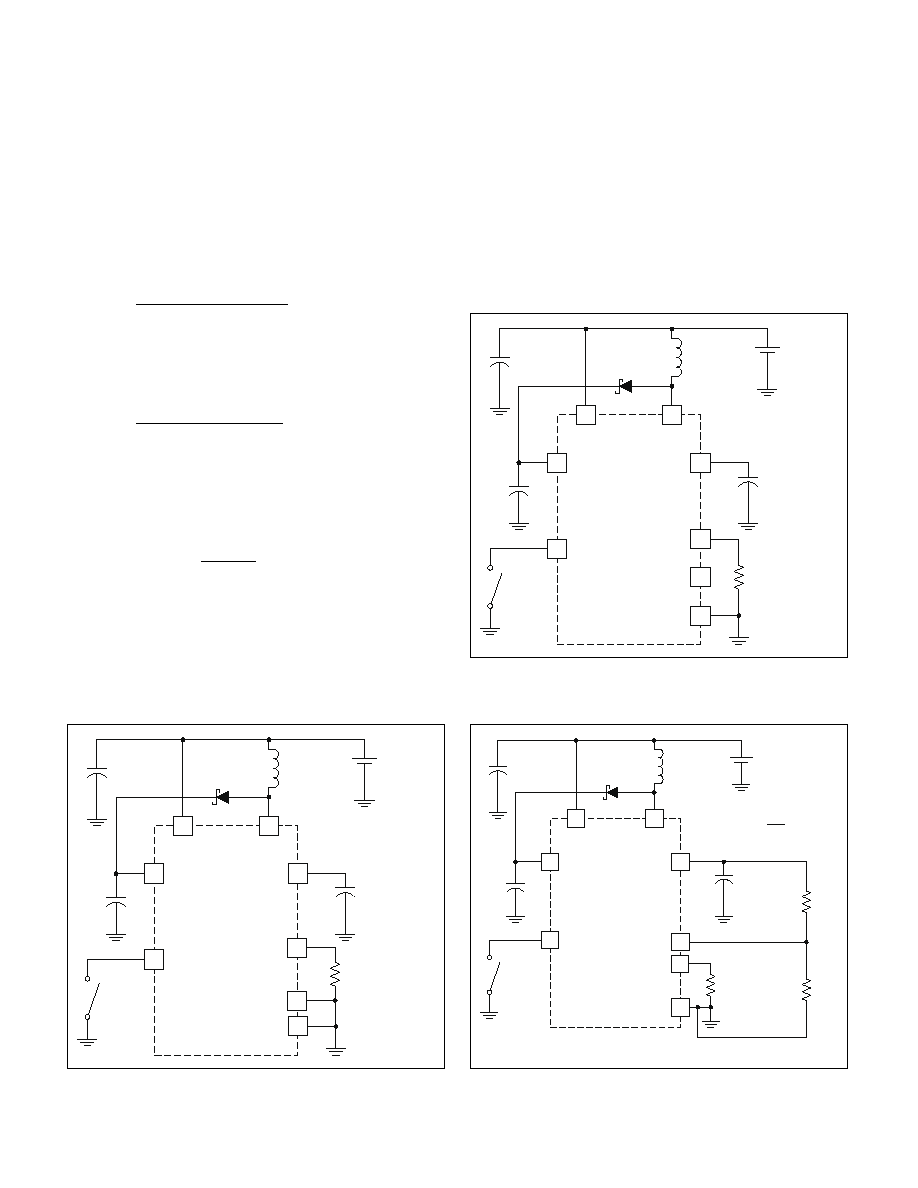
APPLICATION INFORMATION (cont.)
5
8
1
7
6
VOUT
SW
10SN100M
100
µ
F
R
PL
6.2
WCR0805-6R207
4
3.3V AT 500mW
2
SD
VGD
10
µ
F
OPEN =
SD
3
VIN
10
µ
F
MMSZ5240BT1
+1V TO 3.5V
DT3316P-223
22
µ
H
PLIM
SGND
PGND
UCC3941-3
8V
Figure 3. Dual output synchronous boost 3.3V
version.
UDG-98163
5
8
1
7
6
VOUT
SW
10SN100M
100
µ
F
R
PL
6.2
WCR0805-6R207
4
5.0V AT 500mW
2
SD
VGD
10
µ
F
OPEN =
SD
3
VIN
10
µ
F
MMSZ5240BT1
+1V TO 5.5V
DT3316P-223
22
µ
H
PLIM
ADJ
PGND
UCC3941-5
8V
Figure 4. Dual output synchronous boost 5V version.
UDG-98159
5
8
1
7
6
VOUT
SW
10SN100M
100
µ
F
R
PL
6.2
WCR0805-6R207
4
3.3V AT 500mW
2
SD
VGD
10
µ
F
OPEN =
SD
3
VIN
10
µ
F
MMSZ5240BT1
+1V TO VOUT + 0.5V
DT3316P-223
22
µ
H
PLIM
SGND
PGND
UCC3941-3
10V
R1
R2
VOUT=1.25(1+
)
R1
R2
Figure 5. Dual output synchronous boost ADJ
version.
UDG-98164

7
UCC2941-3/-5/-ADJ
UCC3941-3/-5/-ADJ
1.0V input.
Inductor Section
An inductor value of 22
µ
H will work well in most applica-
tions, but values between 10
µ
H and 100
µ
H are also ac-
ceptable. Lower value inductors typically offer lower ESR
and smaller physical size. Due to the nature of the
"bang-bang" controllers, larger inductor values will typi-
cally result in larger overall voltage ripple, because once
the output voltage level is satisfied the converter goes
discontinuous, resulting in the residual energy of inductor
causing overshoot.
It is recommended to keep the ESR of the inductor below
0.15
for 500mW applications. A Coilcraft DT3316P-223
surface mount inductor is one choice since it has a cur-
rent rating of 1.5A and an ESR of 84m
. Other choices
for surface mount inductors are shown in Table 1.
Output Capacitor Selection
Once the inductor value is selected the capacitor value
will determine the ripple of the converter. The worst case
peak to peak ripple of a cycle is determined by two com-
ponents, one is due to the charge storage characteristic,
and the other is the ESR of the capacitor. The worst case
ripple occurs when the inductor is operating at maximum
current and is expressed as follows:
( )
(
)
V
I
L
C
V
V
I
C
CL
O
I
CL
ESR
=
∑
∑ ∑
-
+
∑
2
2
where
I
CL
= the peak inductor current
I
Power Limit
V
CL
IN
=
V = output ripple
V
O
= output voltage
V
I
= input voltage
C
ESR
= ESR of the output capacitor
A Sanyo OS-CON series surface mount capacitor
(10SN100M) is one recommendation. This part has an
ESR rating of 90m
at 100
µ
F. Other potential capacitor
sources are shown in Table 2.
Input Capacitor Selection
Since the UCC3941 family does not require a large de-
coupling capacitor on the input voltage to operate prop-
erly, a 10
µ
F capacitor is sufficient for most applications.
Optimum efficiency will occur when the capacitor value is
large enough to decouple the source impedance. This
usually occurs for capacitor values in excess of 100
µ
F.
APPLICATION INFORMATION (cont.)
MANUFACTURER
PART NUMBER
Sanyo Video
Components
San Diego, California
OS-CON Series
Tel: 619-661-6322
Fax: 619-661-1055
AVX
Sanford, Maine
TPS Series
Tel: 207-282-5111
Fax: 207-283-1941
Sprague
Concord, New Hampshire
695D Series
Tel: 603-224-1961
Table 2. Capacitor Suppliers
MANUFACTURER
PART NUMBERS
Coilcraft
Cary, Illinois
DT Series
Tel: 708-639-2361
Fax: 708-639-1469
Coiltronics
Boca Raton, Florida
CTX Series
Tel: 407-241-7876
Table 1. Inductor Suppliers

8
UCC2941-3/-5/-ADJ
UCC3941-3/-5/-ADJ
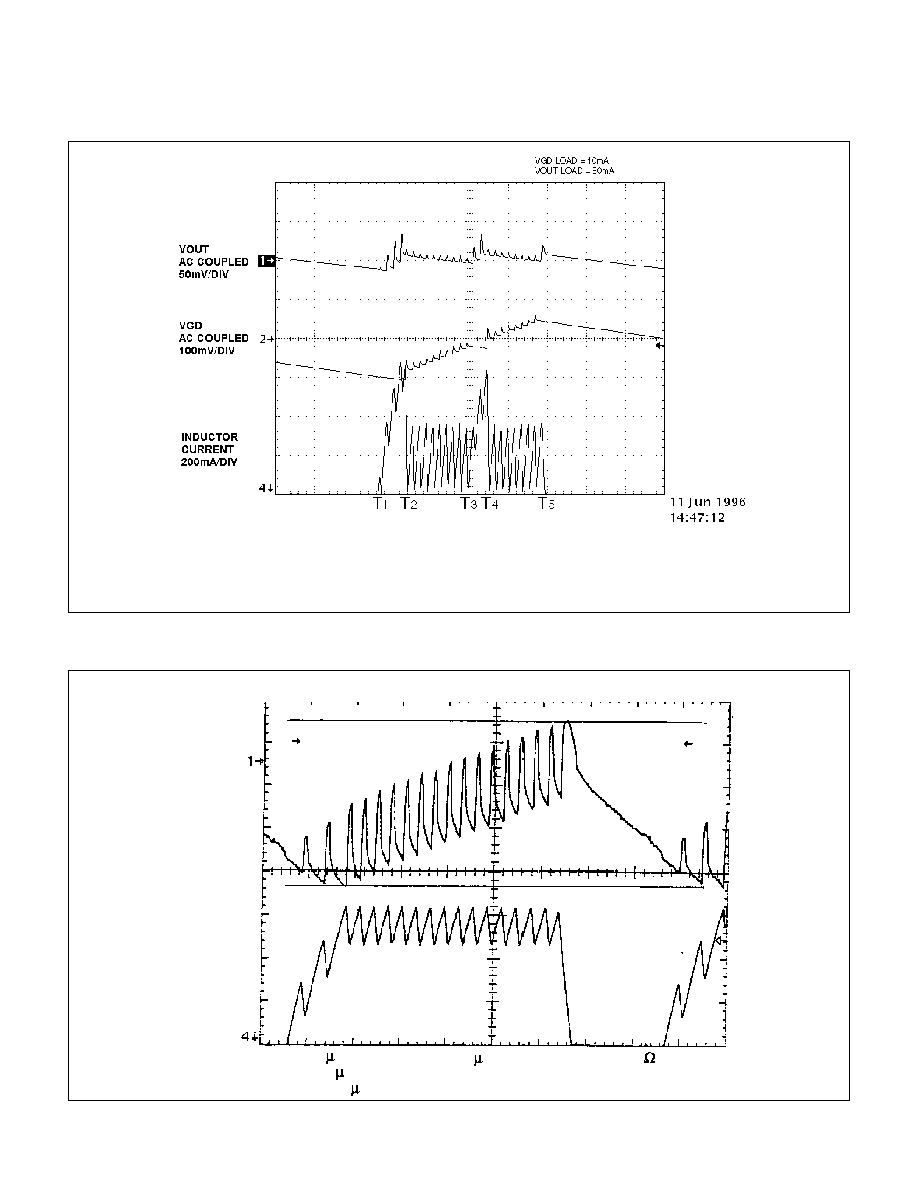
Figure 8. Startup characteristics.
T
0
:
200kHz startup oscillator starts VGD rising.
T
1
:
VGD gets to a sufficient voltage (5V) to run IC in normal operating mode.
T
2
:
VGD has reached a sufficient voltage (7.5V) to get VOUT started.
T
3
:
VOUT is serviced and starting up.
T
4
:
VOUT has reached a sufficient voltage and VGD is serviced until it reaches = 8.5V.
0
10
20
30
40
50
60
70
80
90
100
0.1
1
10
100
IOUT (mA)
EFFICIENCY
(%)
VIN= 2V
VIN= 2.5V
VIN= 3V
Figure 7. UCC3941 Efficiency vs. I
OUT
, V
OUT
= 3.3V.
0
10
20
30
40
50
60
70
80
90
0.1
1
10
100
IOUT (mA)
EFFICIENCY
(%)
VIN = 1V
VIN = 1.25V
VIN = 1.5V
Figure 6. UCC3941 Efficiency vs. I
OUT
, V
OUT
= 3.3V.
9
UCC2941-3/-5/-ADJ
UCC3941-3/-5/-ADJ
Figure 10. Pseudo continuous mode operation.
VOUT RIPPLE
20mV/DIV
I
INDUCTOR
CURRENT
0.2A/DIV
L = 22 H
C = 100 F
C
VGD
= 22 H
R
PL
= 6
V
IN
= 1.25
I
OUT
= 100mA
20 s/DIV
Figure 9. Dual output example.
APPLICATION INFORMATION (cont.)
T
1
:
VOUT is service and inductor current goes continuous.
T
2
:
VGD is serviced with discontinuous operation and reaches 1st threshold (7.5V).
T
3
:
VOUT requires servicing so since VGD has at least reached its first threshold of 7.5V the VOUT has priority.
T
4
:
VOUT is satisfied and VGD is serviced until 2nd threshold is reached.
T
5
:
Both outputs are satisfied.
10
UCC2941-3/-5/-ADJ
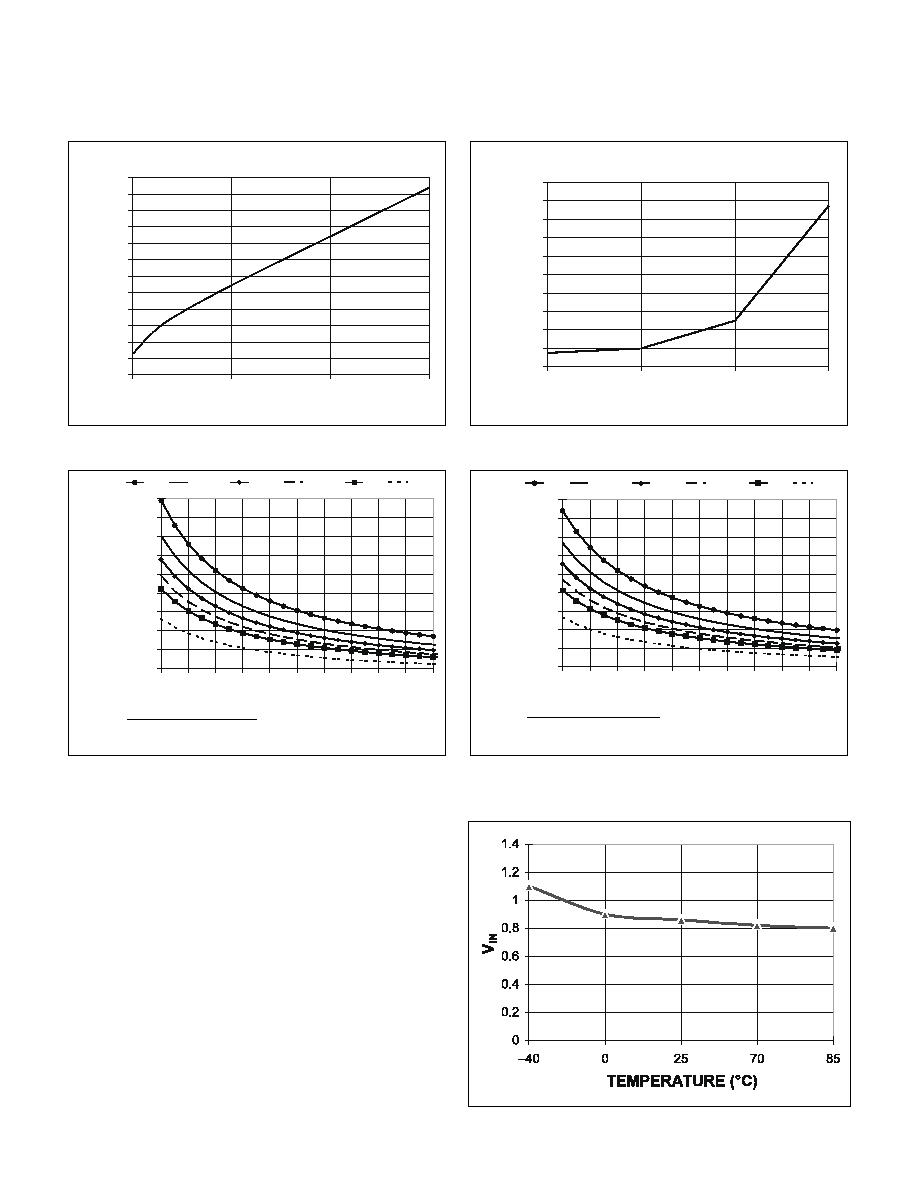
UCC3941-3/-5/-ADJ
0.300
0.500
0.700
0.900
1.100
1.300
1.500
1.700
1.900
2.100
0
2
4
6
8
10
12
14
16
18
20
R
P
(
)
I
LIM
(A)
1V
1.25V
1.5V
1.75V
2V
3V
Figure 13. UCC3941-ADJ I
LIM
vs. R
P
(J package only).
0.300
0.500
0.700
0.900
1.100
1.300
1.500
1.700
1.900
2.100
0
2
4
6
8
10
12
14
16
18
20
R
P
(
)
I
LIM
(A)
1V
1.25V
1.5V
1.75V
2V
3V
Figure 14. UCC3941-ADJ I
LIM
vs. R
P
(all other
packages).
UNITRODE CORPORATION
7 CONTINENTAL BLVD. ∑ MERRIMACK, NH 03054
TEL. (603) 424-2410 FAX (603) 424-3460
( )
(
)
(
)
IL
R
V
Rp
P
BAT
=
+
∑
+
11 5
6 1
0 2
.
.
.
( )
(
)
(
)
IL
R
V
Rp
P
BAT
=
+
∑
+
11 8
6 7
0 26
.
.
.
0
0.1
0.2
0.3
0.4
0.5
0.6
0.7
0.8
0.9
1
1.1
1.2
0
50
100
150
I
OUT
(mA)
VBA
T
a
t
D
R
O
POUT
(V)
Figure 11. UCC3941-3 Dropout vs. I
OUT
.
APPLICATION INFORMATION (cont.)
0.8
0.84
0.88
0.92
0.96
1
1.04
1.08
1.12
1.16
1.2
0
50
100
150
I
OUT
(mA)
V
ST
AR
T
(V)
Figure 12. Minimum start voltage vs. I
OUT
.
Figure 15. V
IN
startup vs. temp.

IMPORTANT NOTICE
Texas Instruments and its subsidiaries (TI) reserve the right to make changes to their products or to discontinue
any product or service without notice, and advise customers to obtain the latest version of relevant information
to verify, before placing orders, that information being relied on is current and complete. All products are sold
subject to the terms and conditions of sale supplied at the time of order acknowledgement, including those
pertaining to warranty, patent infringement, and limitation of liability.
TI warrants performance of its semiconductor products to the specifications applicable at the time of sale in
accordance with TI's standard warranty. Testing and other quality control techniques are utilized to the extent
TI deems necessary to support this warranty. Specific testing of all parameters of each device is not necessarily
performed, except those mandated by government requirements.
CERTAIN APPLICATIONS USING SEMICONDUCTOR PRODUCTS MAY INVOLVE POTENTIAL RISKS OF
DEATH, PERSONAL INJURY, OR SEVERE PROPERTY OR ENVIRONMENTAL DAMAGE ("CRITICAL
APPLICATIONS"). TI SEMICONDUCTOR PRODUCTS ARE NOT DESIGNED, AUTHORIZED, OR
WARRANTED TO BE SUITABLE FOR USE IN LIFE-SUPPORT DEVICES OR SYSTEMS OR OTHER
CRITICAL APPLICATIONS. INCLUSION OF TI PRODUCTS IN SUCH APPLICATIONS IS UNDERSTOOD TO
BE FULLY AT THE CUSTOMER'S RISK.
In order to minimize risks associated with the customer's applications, adequate design and operating
safeguards must be provided by the customer to minimize inherent or procedural hazards.
TI assumes no liability for applications assistance or customer product design. TI does not warrant or represent
that any license, either express or implied, is granted under any patent right, copyright, mask work right, or other
intellectual property right of TI covering or relating to any combination, machine, or process in which such
semiconductor products or services might be or are used. TI's publication of information regarding any third
party's products or services does not constitute TI's approval, warranty or endorsement thereof.
Copyright
©
1999, Texas Instruments Incorporated