
UCC2941-3, UCC2941-5, UCC2941-ADJ, UCC3941-3, UCC3941-5, UCC3941-ADJ
1 V SYNCHRONOUS BOOST CONVERTER
SLUS242B ≠ JANUARY 1999 ≠ REVISED JUNE 2001
1
www.ti.com
D
1-V Input Voltage Operation Start-up
Ensured Under Full Load on Main Output
With Operation Down to 0.4 V
D
Input Voltage Range of 1 V to V
OUT
+ 0.5 V
D
500-mW Output Power at Battery Voltages
as Low as 0.8 V
D
Secondary 9-V Supply From a Single
Inductor
D
Adjustable Output Power Limit Control
D
Output Fully Disconnected in Shutdown
D
Adaptive Current-Mode Control for
Optimum Efficiency
D
8-
µ
A Shutdown Supply Current
description
The UCC3941 family of low-input-voltage single-inductor boost-converters are optimized to operate from a
single- or dual-alkaline cell, and step up to a 3.3-V, 5-V, or an adjustable output at 500 mW. The UCC3941 family
also provides an auxiliary 9-V, 100-mW output, primarily for the gate drive supply, which can be used for
applications requiring an auxiliary output such as a 5-V supply by linear regulating. The primary output starts
up under full load at input voltages typically as low as 0.8 V, with a guaranteed maximum of 1 V, and operates
down to 0.4 V once the converter is operating, maximizing battery utilization.
Demanding applications such as pagers and personal digital assistants require high efficiency from several
milliwatts to several hundred milliwatts, and the UCC3941 family accommodates these applications with > 80%
typical efficiencies over the wide range of operation. The high-efficiency at low-output current is achieved by
optimizing switching and conduction losses along with low-quiescent current. At higher output current the
0.25-
charge switch, and the 0.4-
synchronous rectifier, along with continuous-mode conduction, provide
high efficiency. The wide input-voltage range on the UCC3941 family can accommodate other power sources
such as NiCd and NiMH.
Other features include maximum power control and shutdown control. The device is available in 8-pin SOIC (D)
and 8-pin DIP (N).
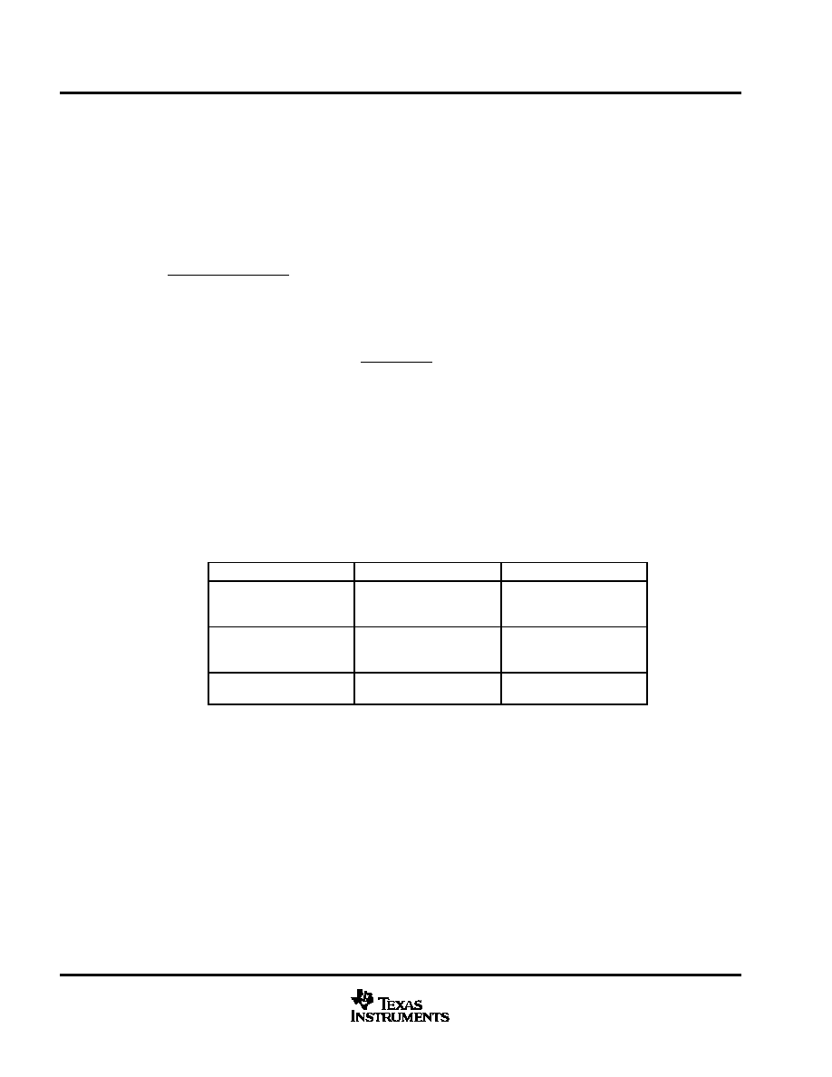
AVAILABLE OPTIONS
PACKAGED DEVICES
SOIC (D)
DIP (N)
TA
VOUT (V)
A
3.3
5.0
Adjustable
(1.3 V to 6 V)
3.3
5.0
Adjustable
(1.3 V to 6 V)
≠40
_
C to 85
_
C
UCC2941D≠3
UCC2941D≠5
UCC2941D≠ADJ
UCC2941N≠3
UCC2941N≠5
UCC2941N≠ADJ
0
_
C to 70
_
C
UCC3941D≠3
UCC3941D≠5
UCC3941D≠ADJ
UCC3941N≠3
UCC3941N≠5
UCC3941N≠ADJ
The SOIC (D) package is available left end taped and reeled. Add an R suffix to the device type (e.g., UCC2941DR≠3) to order
quantities of 2500 devices per reel.
Copyright
2001, Texas Instruments Incorporated
PRODUCTION DATA information is current as of publication date.
Products conform to specifications per the terms of Texas Instruments
standard warranty. Production processing does not necessarily include
testing of all parameters.
Please be aware that an important notice concerning availability, standard warranty, and use in critical applications of
Texas Instruments semiconductor products and disclaimers thereto appears at the end of this data sheet.
D OR N PACKAGE
(TOP VIEW)
1
2
3
4
8
7
6
5
VOUT
VGD
VIN
SD
SW
PGND
SGND
PLIM
1
2
3
4
8
7
6
5
VOUT
VGD
VIN
SD
SW
PGND
FB
PLIM
UCC3941≠ADJ ONLY
(TOP VIEW)

UCC2941-3, UCC2941-5, UCC2941-ADJ, UCC3941-3, UCC3941-5, UCC3941-ADJ
1 V SYNCHRONOUS BOOST CONVERTER
SLUS242B ≠ JANUARY 1999 ≠ REVISED JUNE 2001
2
www.ti.com
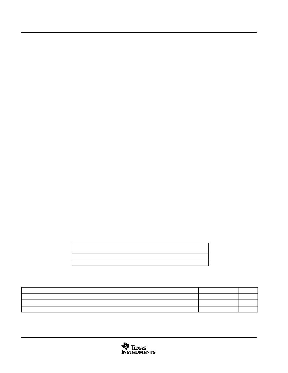
functional block diagram
UDG≠98147
MODULATOR CONTROL CIRCUIT
4
5
6
7
1
8
3
2
1.25 V
UCC3941≠ADJ
OPEN = SD
SD
10
µ
F
VGD
8.5 V
STARTUP
CIRCUITRY
VIN
SW
+
10
µ
F
22
µ
H
100
µ
F
0.4
VOUT
PGND
PLIM
0.25
UCC3941≠3 = 3.3 V
UCC3941≠5 = 5.0 V
UCC3941≠ADJ = 1.30 V TO 6 V
FOR UCC3941
≠
ADJ ONL
Y
+
{
SGND/FB
S
SYNCHRONOUS RECTIFICATION CIRCUITRY
S
ANTI≠CROSS CONDUCTION STARTUP
S
MULTIPLEXING LOGIC
S
MAXIMUM INPUT POWER CONTROL
S
ADAPTIVE CURRENT CONTROL
0.8 V TO VOUT+0.5 V
For UCC3941≠ADJ only: Pin 7 = SGND & PGND, Pin 6 = output sense feedback, FB

UCC2941-3, UCC2941-5, UCC2941-ADJ, UCC3941-3, UCC3941-5, UCC3941-ADJ
1 V SYNCHRONOUS BOOST CONVERTER
SLUS242B ≠ JANUARY 1999 ≠ REVISED JUNE 2001
3
www.ti.com
Terminal Functions
TERMINAL
NO.
NAME
UCC2941≠3
UCC2941≠5
UCC3941≠3
UCC3941≠5
UCC2941≠ADJ
UCC3941≠ADJ
I/O
DESCRIPTION
FB
≠
6
I
Feedback control pin used in the UCC3941≠ADJ version only. The internal
reference for this comparator is 1.25V and external resistors provide the gain to
the output voltage.
PGND
7
7
≠
Power ground of the IC. The inductor charging current flows through this pin. For
the UCC3941≠ADJ signal ground and power ground lines are tied to a common
pin.
PLIM
5
5
I
Peak current limit
SGND
6
≠
≠
Signal ground of the IC. For the UCC3941≠ADJ signal ground and power ground
lines are tied to a common pin
SD
4
4
I
Shutdown pin
SW
8
8
I
Inductor connection
VGD
2
2
O
Gate drive supply
VIN
3
3
I
Input voltage to supply the IC during startup. After the output is running the IC
draws power from VOUT or VGD
VOUT
1
1
O
Main output voltage
detailed description
peak limit (PLIM)
The PLIM pin is programmed to set the maximum input power for the converter. For example a 1-A current limit
at 1 V would have a 333-mA limit at 3 V input keeping the input power constant at 1 W. The peak current at
VIN = 1 V is programmed to 1.5 A (1.5 W) when this pin is grounded. The power limit is given by:
PL
W
+
11.8
n
R
PL
)
6.7
)
V
IN
0.26
where R
PL
is equal to the external resistor from the PLIM pin to ground and n is the expected efficiency of the
converter. The peak current limit is given by:
I
PK(A)
+
11.8
n
V
IN
R
PL
)
6.7
)
0.26
Constant power gives several advantages over constant current such as lower output ripple.
shutdown (SD)
When the SD pin is open, the built-in 7-
µ
A current source pulls up on the pin and programs the IC to go into
shutdown mode. This pin requires an open circuit for shutdown and does not operate correctly when driven to
a logic level high with TTL or CMOS logic. When this pin is connected to ground, (either directly or with a
transistor) the IC is enabled and both output voltages regulate.
(1)
(2)
UCC2941-3, UCC2941-5, UCC2941-ADJ, UCC3941-3, UCC3941-5, UCC3941-ADJ
1 V SYNCHRONOUS BOOST CONVERTER
SLUS242B ≠ JANUARY 1999 ≠ REVISED JUNE 2001
4
www.ti.com
detailed description (continued)
needs a name (SW)
The SW pin inductor is connected between this node and VIN. The VGD (gate drive supply) flyback diode is
also connected to this pin. When servicing the 3.3-V supply, this pin goes low charging the inductor, then shut
off, dumping the energy through the synchronous rectifier to the output. When servicing the VGD supply, the
internal synchronous rectifier stays off, and the energy is diverted to VGD through the flyback diode. During
discontinuous portions of the inductor current a MOSFET resistively connects VIN to SW damping excess
circulating energy to eliminate undesired high frequency ringing.
gate drive supply (VGD)
The VGD pin is coarsely regulated around 9 V, and is primarily used for the gate drive supply for the power
switches in the IC. This pin can be loaded with up to 10 mA as long as it does not present a load at voltages
below 2 V. This ensures proper startup of the IC. The VGD supply can go as low as 7.5 V without interfering
with the servicing of the 3.3-V output. Below 7.5 V, VGD has the highest priority, although in practice the voltage
should not decay to that level if the output capacitor is sized properly.
output voltage (VOUT)
Main output voltage (3.3 V, 5 V, or adjustable) which has highest priority in the multiplexing scheme, as long
as VGD is above the critical level of 7.5 V. Loads over 150 mA are achievable at an input voltage of 1-V. This
output starts up with 1-V input at full load.
absolute maximum ratings over operating free≠air temperature range (unless otherwise noted)
Input voltage VIN, PLIM
≠0.3 V to 10 V
. . . . . . . . . . . . . . . . . . . . . . . . . . . . . . . . . . . . . . . . . . . . . . . . . . . . . . . . . . . .
Voltage range, VGD, SW
≠0.3 V to 15 V
. . . . . . . . . . . . . . . . . . . . . . . . . . . . . . . . . . . . . . . . . . . . . . . . . . . . . . . . . . .
Voltage range, SD
≠0.3 V to VIN
. . . . . . . . . . . . . . . . . . . . . . . . . . . . . . . . . . . . . . . . . . . . . . . . . . . . . . . . . . . . . . . . . .
Output voltage range, VOUT
≠0.3 V to 10 V
. . . . . . . . . . . . . . . . . . . . . . . . . . . . . . . . . . . . . . . . . . . . . . . . . . . . . . . .
Operating virtual junction temperature range, T
J
≠55
_
C to 150
_
C
. . . . . . . . . . . . . . . . . . . . . . . . . . . . . . . . . . . . . .
Storage temperature range, T
stg
≠65
_
C to 150
_
C
. . . . . . . . . . . . . . . . . . . . . . . . . . . . . . . . . . . . . . . . . . . . . . . . . . . .
Lead temperature soldering 1,6 mm (1/16 inch) from case for 10 seconds
300
_
C
. . . . . . . . . . . . . . . . . . . . . . .
CDM 1 kV
. . . . . . . . . . . . . . . . . . . . . . . . . . . . . . . . . . . . . . . . . . . . . . . . . . . . . . . . . . . . . . . . . . . . . . .
Stresses beyond those listed under "absolute maximum ratings" may cause permanent damage to the device. These are stress ratings only, and
functional operation of the device at these or any other conditions beyond those indicated under "recommended operating conditions" is not
implied. Exposure to absolute≠maximum≠rated conditions for extended periods may affect device reliability. Currents are positive into, negative
out of the specified terminal.
DISSIPATION RATING TABLE
PACKAGE
TA
25
_
C
POWER RATING
DERATING FACTOR
ABOVE TA = 25
_
C
TA = 85
_
C
POWER RATING
D
760 mW
6.1 mW/
_
C
390 mW
N
980 mW
7.9 mW/
_
C
510 mW
recommended operating conditions
MIN
MAX
UNIT
Input voltage
0.8
5.0
V
Output voltage
1.8
5.5
V
Output current
0
200
mA

UCC2941-3, UCC2941-5, UCC2941-ADJ, UCC3941-3, UCC3941-5, UCC3941-ADJ
1 V SYNCHRONOUS BOOST CONVERTER
SLUS242B ≠ JANUARY 1999 ≠ REVISED JUNE 2001
5
www.ti.com
electrical characteristics over recommended operating junction temperature range, for UCC3941,
T
A
= 0
_
C to 70
_
C, for UCC2941, T
A
= ≠40
_
C to 85
_
C, VIN = 1.25 V, T
A
= T
J
(unless otherwise noted)
input voltage
PARAMETER
TEST CONDITIONS
MIN
TYP
MAX
UNIT
TJ = 25
_
C,
No external VGD load,
IOUT = 100 mA,
See Note 1
0.8
1.0
V
Minumum startup voltage
TJ = 0
_
C to 85
_
C, No external VGD load,
IOUT = 100 mA,
See Note 1
0.9
1.1
V
TJ = ≠40
_
C to 0
_
C, No external VGD load,
IOUT = 100 mA,
See Note 1
0.9
1.5
V
Minumum dropout voltage
IOUT = 0 mA,
No external VGD load,
VGD = 6.3 V
0.5
V
Input voltage range
1
VOUT
+ 0.5
V
Quiescent supply current
See note 2
13
25
µ
A
Shutdown supply current
SD = open
8
20
µ
A
output voltage
PARAMETER
TEST CONDITIONS
MIN
TYP
MAX
UNIT
Quiescent supply current
See note 2
32
80
µ
A
Shutdown supply current
SD = open
6
15
µ
A
1 V < VIN < 3 V
3.18
3.25
3.37
V
Regulation voltage
UCC3941≠3
1 V < VIN < 3 V,
0 mA < IOUT < 150 mA,
See Note 1
3.17
3.30
3.43
V
Regulation voltage
1 V < VIN < 5 V
4.85
5.00
5.15
V
UCC3941≠5
1 V < VIN < 5 V,
0 mA < IOUT < 100 mA,
See Note 1
4.8
5.0
5.2
V
Feedback voltage
UCC3941≠ADJ
1 V < VIN < 3 V
1.212
1.250
1.288
V
VGD output
PARAMETER
TEST CONDITIONS
MIN
TYP
MAX
UNIT
Quiescent supply current
See note 2
25
60
µ
A
Shutdown supply current
SD = open
8
20
µ
A
1 V < VIN < 3 V
7.5
8.7
9.2
V
Regulation voltage
1 V < VIN < 3 V,
0 mA < IOUT < 10 mA,
See Note 1
7.4
87
9.3
V
NOTE 1: Performance from application circuit shown in Figures 3, 4, and 5. Ensured by design. Not 100% production tested.
NOTE 2: For the UCC3941≠3, VOUT = 3.47 V and VGD = 9.3 V. For the UCC3941≠5, VOUT = 5.25 V, VGD = 9.3 V. For the UCC3941≠ADJ,
FB = 1.315 V, VGD = 9.3 V.

UCC2941-3, UCC2941-5, UCC2941-ADJ, UCC3941-3, UCC3941-5, UCC3941-ADJ
1 V SYNCHRONOUS BOOST CONVERTER
SLUS242B ≠ JANUARY 1999 ≠ REVISED JUNE 2001
6
www.ti.com
electrical characteristics over recommended operating junction temperature range, for UCC3941,
T
A
= 0
_
C to 70
_
C, for UCC2941, T
A
= ≠40
_
C to 85
_
C, VIN = 1.25 V, T
A
= T
J
(unless otherwise noted)
(continued)
inductor charging (L = 22
µ
H)
PARAMETER
TEST CONDITIONS
MIN
TYP
MAX
UNIT
Peak discontinuous current
Over operating range
0.05
0.85
A
Peak continuous current
RPLIM = 6.2
,
See Note 1
0.5
0.9
1.3
A
Charge switch RDS(on)
N and D package, I = 200 mA
0.25
0.40
Current limit delay
See Note 1
50
ns
synchronous rectifier
PARAMETER
TEST CONDITIONS
MIN
TYP
MAX
UNIT
UCC3941N≠ADJ
UCC3941D≠ADJ
I = 200 mA,
VOUT = 3.3 V
0.35
0.6
Rectifier RDS(on)
UCC3941N≠3
UCC3941D≠3
I = 200 mA
0.35
0.6
UCC3941N≠5
UCC3941D≠5
I = 200 mA
0.5
0.8
shutdown
PARAMETER
TEST CONDITIONS
MIN
TYP
MAX
UNIT
Shutdown bias current
SD = 0 V
≠10
≠7
µ
A
NOTE 1: Performance from application circuit shown in Figures 3, 4, and 5. Ensured by design. Not 100% production tested.
NOTE 2: For the UCC3941≠3, VOUT = 3.47 V and VGD = 9.3 V. For the UCC3941≠5, VOUT = 5.25 V, VGD = 9.3 V. For the UCC3941≠ADJ,
FB = 1.315 V, VGD = 9.3 V.
UCC2941-3, UCC2941-5, UCC2941-ADJ, UCC3941-3, UCC3941-5, UCC3941-ADJ
1 V SYNCHRONOUS BOOST CONVERTER
SLUS242B ≠ JANUARY 1999 ≠ REVISED JUNE 2001
7
www.ti.com
APPLICATION INFORMATION
A detailed block diagram of the UCC3941 is shown in Figure 1. Unique control circuitry provides high-efficiency
power conversion for both light and heavy loads by transitioning between discontinuous and continuous
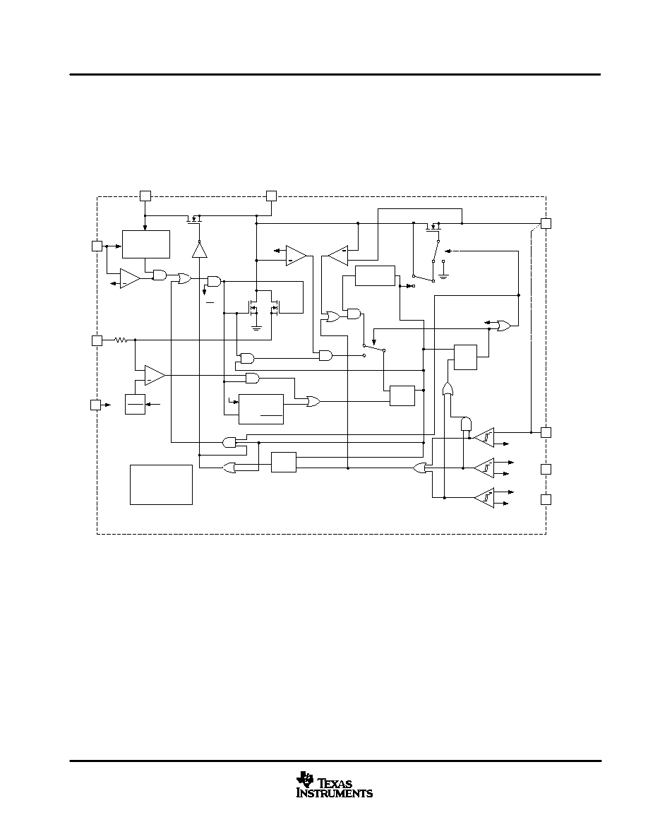
conduction based on load conditions. Figure 2 depicts converter waveforms for the application circuit shown
in Figure 3. A single 22-
µ
H inductor provides the energy pulses required for a highly efficient 3.3-V converter
at up to 500 mW output power.
UDG≠98146
4
5
2
3
8
1
6
6
7
SD
PLIM
VGD
VIN
SW
VOUT
FB
(UCC3941≠ADJ
ONLY)
PGND
SGND
(UCC3941≠3/≠5
ONLY)
5
VGD
* 3.3 V FOR UCC3941≠3
5.0 V FOR UCC3941≠5
1.25 V FOR UCC3941≠ADJ
VGD
** 8.7 V FOR UCC3941≠3
9.6 V FOR UCC3941≠5/≠ADJ
VGD
*** 7.7 V FOR UCC3941≠3
8.8 V FOR UCC3941≠5/≠ADJ
FROM
SD
5V
1.1 A
MAX
CURRENT
LIMIT
50 mV
VIN
VIN
SD
50 mV
MAXIMUM
200 kHz
STARTUP
OSCILLATOR
AND CONTROL
VGD
VGD
VGD ZERO
DETECT
VOUT ZERO
DETECT
ANTI≠RINGING
SWITCH
1.7
µ
S
OFF TIME
CONTROLLER
RECTIFIER
CONTROL
FROM SD
CLK
D
Q
L1
R
Q
SD
BOOST
LATCH
ON TIME
CONTROLLER
T
ON
=
11
µ
SEC
VIN
VSAT
*
**
***
THERMAL
SHUTDOWN
R
Q
SD
+
+
+
+
+
+
+
NOTE: Switches are shown in the logic low state; external RPLIM = 6.2
Figure 1. 1≠V Synchronous Boost
UCC2941-3, UCC2941-5, UCC2941-ADJ, UCC3941-3, UCC3941-5, UCC3941-ADJ
1 V SYNCHRONOUS BOOST CONVERTER
SLUS242B ≠ JANUARY 1999 ≠ REVISED JUNE 2001
8
www.ti.com
APPLICATION INFORMATION
UDG≠96117
Figure 2. Inductor Current and Output Ripple Waveforms
At time t1, the 3.3-V output drops below its lower threshold, and the inductor is charged with an on time
determined by:
t
ON
+
12
m
s
VIN
For a 1.25-V input, and a 22-
µ
H inductor, the resulting peak current is approximately 500 mA. At time t2, the
inductor begins to discharge with a minimum off time of 1.7
µ
s. Under lightly loaded conditions, the amount of
energy delivered in this single pulse satisfies the voltage-control loop, and the converter does not command
any more energy pulses until the output again drops below the lower voltage threshold.
At time t3, the VGD supply has dropped below its lower threshold, but the output voltage is still above its
threshold point. This results in an energy pulse to the gate drive supply at t4. However, while the gate drive is
being serviced, the output voltage has dropped below its lower threshold, so the state machine commands an
energy pulse to the output as soon as the gate drive pulse is completed.
Time t6, represents a transition between light and heavy load. A single energy pulse is not sufficient to force
the output voltage above its upper threshold before the minimum off-time has expired, and a second charge
cycle is commanded. Since the inductor current does not reach zero in this case, the peak current is greater
than 0.5 A at the end of the next charge on time. This results in a ratcheting of the inductor current until either
the output voltage is satisfied, or the converter reaches its programmed current limit. At time t7, the gate drive
voltage has dropped below its threshold but the converter continues to service the output because it has highest
priority, unless VGD drops below 7.5 V.
Between t7 and t8, the converter reaches its peak current limit which is determined by R
PL
and VIN. Once the
limit is reached, the converter operates in continuous mode with approximately 200 mA of ripple current. At time
t8, the output voltage is satisfied, and the converter can service VGD, which occurs at t9.
(3)

UCC2941-3, UCC2941-5, UCC2941-ADJ, UCC3941-3, UCC3941-5, UCC3941-ADJ
1 V SYNCHRONOUS BOOST CONVERTER
SLUS242B ≠ JANUARY 1999 ≠ REVISED JUNE 2001
9
www.ti.com
APPLICATION INFORMATION
programming the power limit
The UCC3941 incorporates an adaptive power limit control that modifies the converter current limit as a function
of input voltage. In order to program the function, the user simply determines the output power requirements
and makes an initial converter efficiency estimate. The programming resistor is chosen by:
R
PL
+
11.8
n
P
OUT
*
0.26
n
V
BAT
*
6.7
Where n is the initial efficiency estimate. For 500 mW of output power, with a 1.0 V input, and an efficiency
estimate of 0.75:
R
PL
+
11.8
0.75
0.5
*
(0.26
0.75
1.0)
*
6.7
+
22
W
For decreasing values of R
PL
, the power limit increases. Therefore, to ensure that the converter can supply
500 mW of output power, a power limiting resistor of less than 22
must be chosen.
P
L
+
V
BAT
I
L
+
11.8
22
)
6.7
)
(1.0
0.26)
+
0.67 W
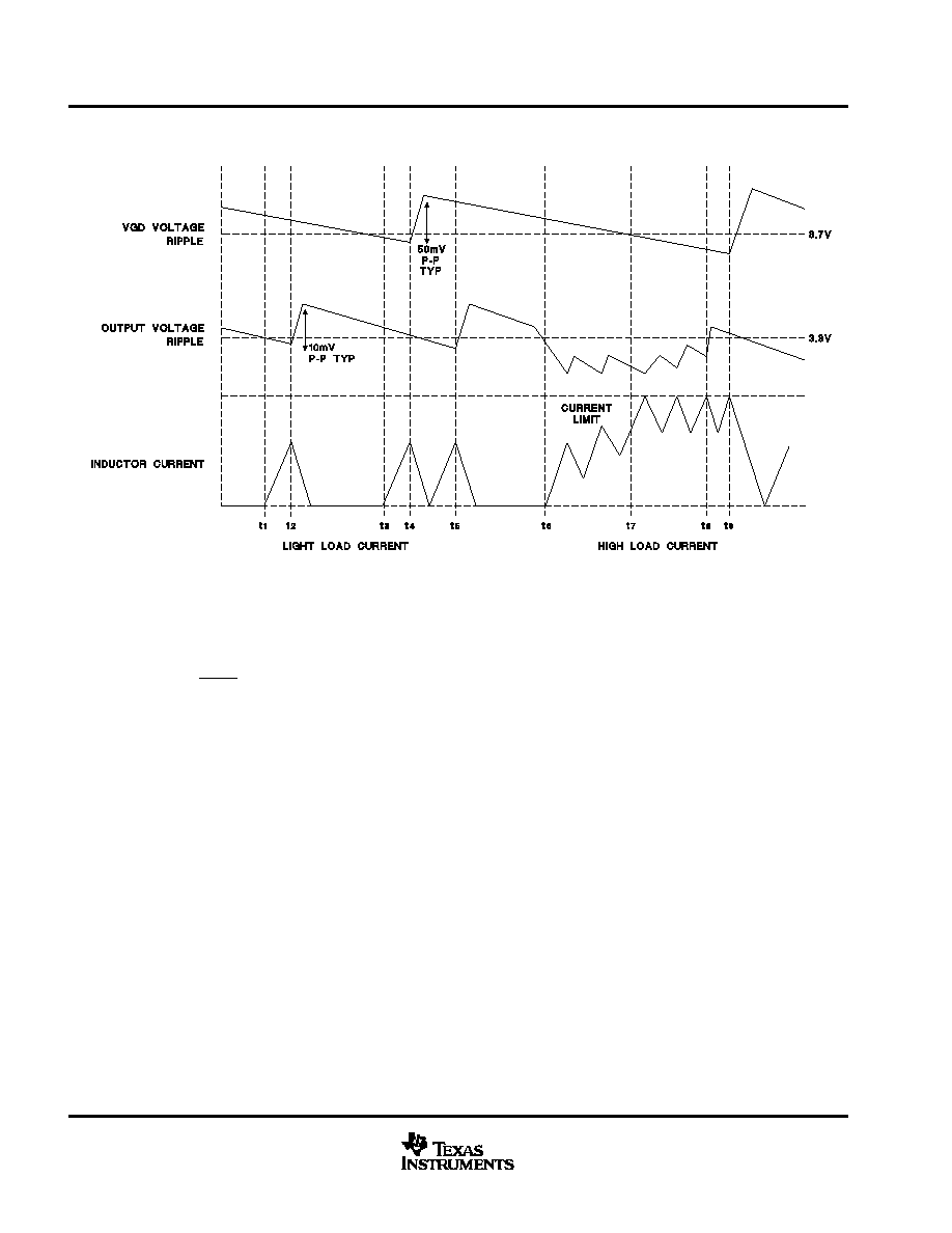
UDG≠98163
5
8
1
7
6
VOUT
SW
10SN100M
100
µ
F
RPL 6.2
WCR0805≠6R207
4
3.3 V AT 500 mW
2
SD
VGD
10
µ
F
OPEN = SD
3
VIN
10
µ
F
MMSZ5240BT1
10 V
+
1 V TO 3.5 V
DT3316P≠223
22
µ
H
PLIM
SGND
PGND
UCC3941≠3
8.5 V
Figure 3. Dual Output Synchronous Boost, 3.3-V Version
(4)
(5)
(6)
UCC2941-3, UCC2941-5, UCC2941-ADJ, UCC3941-3, UCC3941-5, UCC3941-ADJ
1 V SYNCHRONOUS BOOST CONVERTER
SLUS242B ≠ JANUARY 1999 ≠ REVISED JUNE 2001
10
www.ti.com
APPLICATION INFORMATION
programming the power limit (continued)
UDG≠98159
5
8
1
7
6
VOUT
SW
10SN100M
100
µ
F
RPL 6.2
WCR0805≠6R207
4
5.0 V AT 500 mW
2
SD
VGD
10
µ
F
OPEN = SD
3
VIN
10
µ
F
MMSZ5240BT1
10 V
+ 1 V TO 5.5 V
DT3316P≠223
22
µ
H
PLIM
SGND
PGND
UCC3941≠5
8.5 V
Figure 4. Dual Output Synchronous Boost, 5-V Version
UDG≠98164
5
8
1
7
6
VOUT
SW
10SN100M
100
µ
F
RPL 6.2
WCR0805≠6R207
4
2
SD
VGD
10
µ
F
OPEN = SD
3
VIN
10
µ
F
MMSZ5240BT1
+ 1 V TO VOUT + 0.5 V
DT3316P≠223
PLIM
FB
(SGND)
PGND
UCC3941≠ADJ
8.5 V
R1
R2
10 V
VOUT
+
1.25
1
)
R1
R2
AT 500 mA
VREF = 1.25 V
22
µ
H
Figure 5. Dual Output Synchronous Boost, Adjustable Version

UCC2941-3, UCC2941-5, UCC2941-ADJ, UCC3941-3, UCC3941-5, UCC3941-ADJ
1 V SYNCHRONOUS BOOST CONVERTER
SLUS242B ≠ JANUARY 1999 ≠ REVISED JUNE 2001
11
www.ti.com
APPLICATION INFORMATION
programming the power limit (continued)
This power limiting setting supports 0.5 W of output power. It should be noted that the power limit equation
contains an approximation which results in slightly less actual input power than the equation predicts. This
discrepancy results from the fact that the average current delivered to the load is less than the peak current set
by the power limit function due to current ripple. However, if the ripple component of the current is kept low, the
power limit equation can be used as an adequate estimate of input power. Furthermore, since an initial efficiency
estimate was required, sufficient margin can be built into this estimate to ensure proper converter operation.
The 6.2-
external power limit resistor (shown in Figures 3, 4, and 5) results in approximately 700 mW of power
capability with a 1.0-V input.
inductor selection
An inductor value of 22
µ
H works well in most applications, but values between 10
µ
H and 100
µ
H are also
acceptable. Lower-value inductors typically offer lower ESR and smaller physical size. Due to the nature of the
bang≠bang controllers, larger inductor values typically results in larger overall voltage ripple, because once the
output voltage level is satisfied the converter goes discontinuous, resulting in the residual energy of inductor
causing overshoot.
It is recommended to keep the ESR of the inductor below 0.15
for 500-mW applications. A Coilcraft
DT3316P≠223 surface mount inductor is one choice since it has a current rating of 1.5 A and an ESR of 84 m
.
Other choices for surface mount inductors are shown in Table 1.
Table 1. Inductor Suppliers
MANUFACTURER
CONTACT INFORMATION
PART NUMBERS
Coilcraft
Cary, Illinois
Tel: (708) 639≠2361 Fax: (708) 639≠1469
DT Series
Coiltronics
Boca Raton, Florida
Tel: (407) 241≠7878
CTX Series
UCC2941-3, UCC2941-5, UCC2941-ADJ, UCC3941-3, UCC3941-5, UCC3941-ADJ
1 V SYNCHRONOUS BOOST CONVERTER
SLUS242B ≠ JANUARY 1999 ≠ REVISED JUNE 2001
12
www.ti.com
APPLICATION INFORMATION
output capacitor selection
Once the inductor value is selected, the capacitor value determines the ripple of the converter. The worst case
peak-to-peak ripple of a cycle is determined by two components, one is due to the charge storage characteristic,
and the other is the ESR of the capacitor. The worst-case ripple occurs when the inductor is operating at
maximum current and is expressed as follows:
D
V
+
I
CL
2
L
2
C
V
O
*
V
I
)
I
CL
C
ESR
where
D
I
CL
= the peak inductor current I
CL
+
Power Limit
V
IN
D
V = output ripple
D
V
O
= output voltage
D
V
I
= input voltage
D
C
ESR
= ESR of the output capacitor
A Sanyo OS≠CON series surface mount capacitor (10SN100M) is one recommendation. This part has an ESR
rating of 90
µ
W at 100
µ
F. Other potential capacitor sources are shown in Table 2.
Table 2. Capacitor Suppliers
MANUFACTURER
CONTACT INFORMATION
PART NUMBERS
Sanyo Video Components
San Diego, California
Tel: (619) 661≠6322
Fax: (619) 661≠1055
OS≠CON Series
AVX
Sanford, Maine
Tel: (207) 282≠5111
Fax: (207) 283≠1941
TPS Series
Sprague
Concord, New Hampshire
Tel: (603) 224≠1961
695D Series
input capacitor selection
Since the UCC3941 family does not require a large decoupling capacitor on the input voltage to operate
properly, a 10-
µ
F capacitor is sufficient for most applications. Optimum efficiency occurs when the capacitor
value is large enough to decouple the source impedance. This usually occurs for capacitor values in excess
of 100
µ
F.
(7)
UCC2941-3, UCC2941-5, UCC2941-ADJ, UCC3941-3, UCC3941-5, UCC3941-ADJ
1 V SYNCHRONOUS BOOST CONVERTER
SLUS242B ≠ JANUARY 1999 ≠ REVISED JUNE 2001
13
www.ti.com
APPLICATION INFORMATION
system shutdown
The UCC3941 is enabled by shorting the SD pin to ground either directly or through a transistor.The UCC3941
is shut down when the SD pin is floated (an internal current source pulls up on the SD pin). Since the SD pin
is not TTL compatible, 0 V enables the part but 3 V or even 5 V does not properly shut down the device.
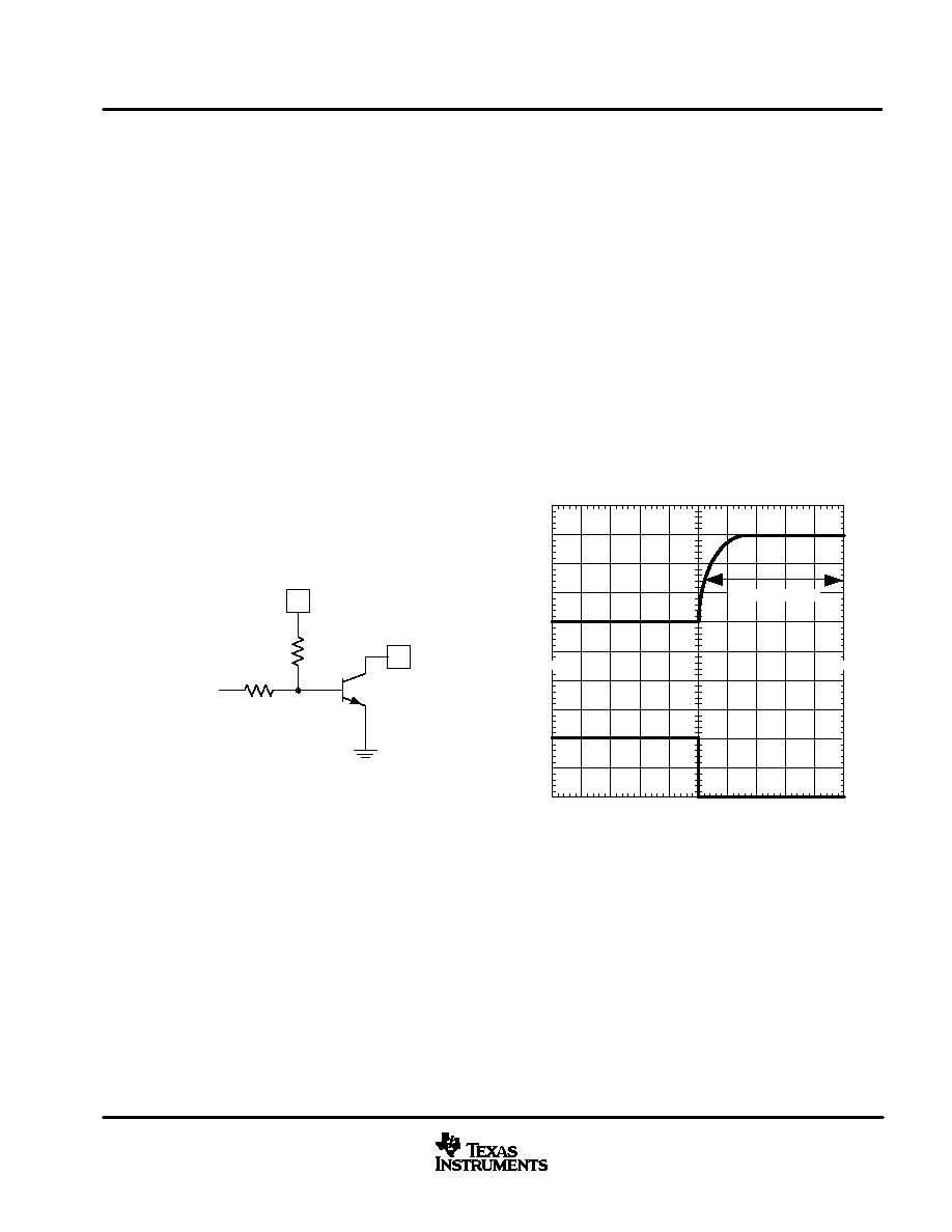
The recommended circuit for a system requiring shutdown control is shown below. The enable line is driven from
a microprocessor or system logic. If enable is low, the SD pin is floated since Q1 base voltage is too low to turn
on. If enable is high, Q1 turns on and SD is grounded, enabling the UCC3941. A 1-M
resistor to VGD allows
Q1 to turn on if the enable pin is high impedance during startup. If shutdown control is not required for the
application, SD should be grounded directly.
CAUTION:
The UCC3941 should be allowed sufficient time to properly shutdown in a controlled
manner. This is accomplished by ensuring that enable is held low at least 500
µ
s before
subsequently being brought high. Not adhering to the timings in Figure 7 can result in
DEVICE FAILURE.
Figure 6
2
4
SD
1 M
VGD
20 k
ENABLE
SHUTDOWN INTERFACE CIRCUIT
500
1000
0
0
~
~
0
2
4
6
8
10
V
SD
≠
Shutdown V
o
ltage
≠
V
Enable V
o
ltage
≠
V
t ≠ Time ≠
µ
s
PROPOGATION DELAY AND RISE TIME
~
~
2
4
6
Ensure 500
µ
s
Figure 7. SD Timings

UCC2941-3, UCC2941-5, UCC2941-ADJ, UCC3941-3, UCC3941-5, UCC3941-ADJ
1 V SYNCHRONOUS BOOST CONVERTER
SLUS242B ≠ JANUARY 1999 ≠ REVISED JUNE 2001
14
www.ti.com
APPLICATION INFORMATION
SD interface circuit
reducing inrush current
A switch mode boost converter requires V
IN
to be less than V
OUT
in order to control current in the inductor.
Forward voltage is applied across the inductor during the t
ON
time (increasing current) while reverse voltage
is applied during the t
OFF
time (decreasing current). During startup, V
OUT
is less than V
IN
, resulting in inrush
current until the output is charged.
The UCC3941 has two outputs; VGD and V
OUT
. Inrush current in a two cell alkaline application is typically higher
than with a single cell and should be minimized to reduce peak currents in the controller. The VGD inrush current
can be minimized by reducing the value of the VGD capacitor. For example a 10-
µ
F capacitor may cause a 3-A
inrush where a 1-
µ
F capacitor results in less than 1-A of inrush. Reducing the V
OUT
inrush current is more
difficult since the output capacitance may need to be large to minimize output ripple. In a two cell application,
a diode from V
IN
to V
OUT
(shown In Figure 8) precharges the V
OUT
capacitor and reduces inrush.
UDG≠00155
8
1
3
SW
VIN
VOUT
2
VGD
10 V
ZENER
+
2 CELL
INPUT
PRECHARGE DIODE
22
µ
H
220
µ
F
1
µ
F
100
µ
F
Figure 8. Optional Precharge Diode for V
OUT
for 2-Cell Input
avoiding inductor saturation
Inductor selection should take into account size, on resistance, and the current capabilities of the part. Inductor
ratings include both saturation current and maximum operating current for the device. The R
PLIM
resistor and
inductor should be selected to guarantee the inductor does not saturate during normal operation. A saturated
inductor can cause excessive peak currents and
i/
t slopes which may result in part failure. Inrush and normal
operating current should be viewed with a current probe and oscilloscope to ensure the inductor current is linear
and controlled.
UCC2941-3, UCC2941-5, UCC2941-ADJ, UCC3941-3, UCC3941-5, UCC3941-ADJ
1 V SYNCHRONOUS BOOST CONVERTER
SLUS242B ≠ JANUARY 1999 ≠ REVISED JUNE 2001
15
www.ti.com
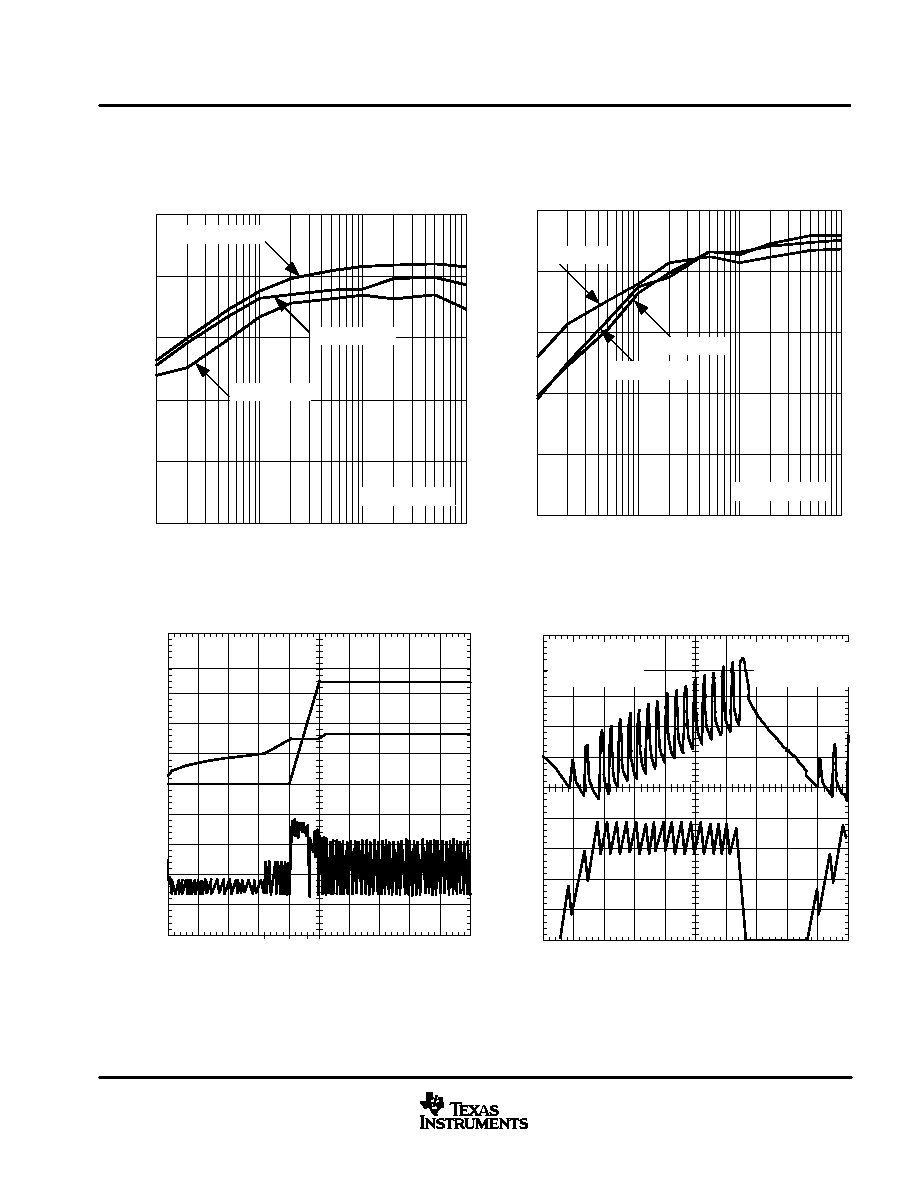
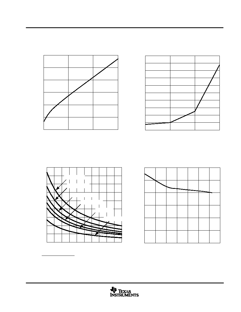
TYPICAL CHARACTERISTICS
Figure 9
Efficiency
≠
%
EFFICIENCY
vs.
OUTPUT CURRENT
0.1
1
10
100
20
40
60
80
100
0
IOUT ≠ Output Current ≠ mA
VIN = 1.5 V
VIN = 1.25 V
VIN = 1 V
VOUT = 3.3 V
Figure 10
Efficiency
≠
%
IOUT ≠ Output Current ≠ mA
EFFICIENCY
vs.
OUTPUT CURRENT
0.1
1
10
100
20
40
60
80
100
0
VIN = 2 V
VIN = 3 V
VIN = 2.5 V
VOUT = 3.3 V
Figure 11
STARTUP CHARACTERISTICS
VOUT
1 V/div
VGD
5 V/div
I L
0.5 A/div
t0
t1
t2
t4
t3
2 ms/ div
3.3 V
VOUT
IL
0.2 A/div
Figure 12
20
µ
s/div
PSUEDO CONTINUOUS MODE OPERATION
VOUT
RIPPLE
20 mV/div
RPL = 6
VIN = 1.25 V
IOUT = 100 mA
L = 22
µ
H
C = 100
µ
F
CVGD = 22
µ
H
UCC2941-3, UCC2941-5, UCC2941-ADJ, UCC3941-3, UCC3941-5, UCC3941-ADJ
1 V SYNCHRONOUS BOOST CONVERTER
SLUS242B ≠ JANUARY 1999 ≠ REVISED JUNE 2001
16
www.ti.com
startup characteristics timing sequence (for single output mode)
(see Figure 11)
D
t0
the 200-kHz srartup oscillator starts VGD rising
D
t1
VGD reaches sufficient voltage (5 V) to run in normal operating mode
D
t2
VGD reaches sufficient voltage (7.5 V) to start VOUT
D
t3
VOUT is serviced and starts up
D
t4
VOUT reaches sufficient voltage and VGD is serviced until it reaches 8.5 V
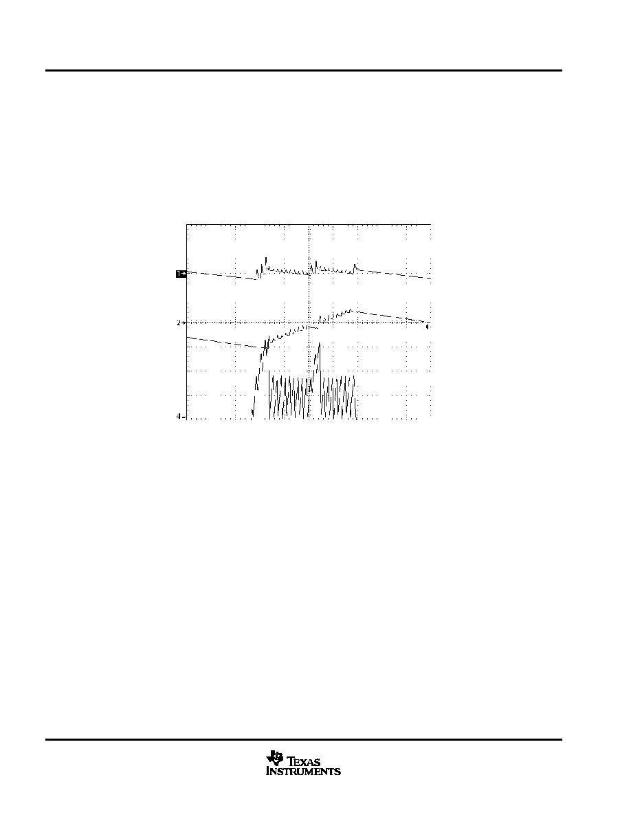
VGD LOAD = 10 mA
VOUT LOAD = 50 mA
t1
t2
t3 t4
t5
VOUT
AC COUPLED
50 mV/DIV
VGD
AC COUPLED
100 mV/DIV
INDUCTOR
CURRENT
200 mA/DIV
Figure 13.
startup characteristics timing sequence (for dual output mode)
(see Figure 13)
D
t1
VOUT is serviced and inductor current goes continuous
D
t2
VGD is serviced with discontinuous operation and reaches its first threshold (7.5 V)
D
t3
VOUT requires servicing and because VGD has reached its minimum threshold of 7.5 V, VOUT
takes priority
D
t4
VOUT is satisfied and VGD is serviced until the second threshold (8.7 V) is reached
D
t5
Both outputs are satisfied
UCC2941-3, UCC2941-5, UCC2941-ADJ, UCC3941-3, UCC3941-5, UCC3941-ADJ
1 V SYNCHRONOUS BOOST CONVERTER
SLUS242B ≠ JANUARY 1999 ≠ REVISED JUNE 2001
17
www.ti.com
TYPICAL CHARACTERISTICS
Figure 14
VIN
≠
Dropout V
o
ltage
≠
V
UCC3941≠3 DROPOUT VOLTAGE
vs.
OUTPUT CURRENT
IOUT ≠ Output Current ≠ mA
0
50
100
150
0.6
1.2
1.0
0.8
0.4
0.2
0
Figure 15
IOUT ≠ Output Current ≠ mA
MINIMUM STARTUP VOLTAGE
vs.
OUTPUT CURRENT
0
0.84
0.80
0.96
0.92
1.04
1.00
1.12
1.08
1.16
50
100
150
0.88
1.20
VIN
≠
Startup V
oltage
≠
V
Figure 16
0
2
4
6
8
10
12
14
16
18
20
0.5
0.3
0.9
0.7
1.3
1.1
1.7
1.5
1.9
2.1
RP ≠ Programming Resistance ≠
UCC3941≠ADJ (N and D PACKAGES) CURRENT LIMIT
vs.
PROGRAMMING RESISTANCE
I L
≠
Current Limit
≠
A
VIN = 1 V
VIN = 1.25 V
VIN = 1.5 V
VIN = 1.75 V
VIN = 2 V
VIN = 3 V
IL
(Rp)
+
11.5
6.7
)
R
P
V
BAT
)
0.26
Figure 17
Temperature ≠
_
C
STARTUP VOLTAGE
vs.
TEMPERATURE
V
IN
≠
Startup V
o
ltage
≠
V
≠40
≠20
0
80
20
100
40
60
0.2
0
0.4
0.6
0.8
1.0
1.2

IMPORTANT NOTICE
Texas Instruments and its subsidiaries (TI) reserve the right to make changes to their products or to discontinue
any product or service without notice, and advise customers to obtain the latest version of relevant information
to verify, before placing orders, that information being relied on is current and complete. All products are sold
subject to the terms and conditions of sale supplied at the time of order acknowledgment, including those
pertaining to warranty, patent infringement, and limitation of liability.
TI warrants performance of its products to the specifications applicable at the time of sale in accordance with
TI's standard warranty. Testing and other quality control techniques are utilized to the extent TI deems necessary
to support this warranty. Specific testing of all parameters of each device is not necessarily performed, except
those mandated by government requirements.
Customers are responsible for their applications using TI components.
In order to minimize risks associated with the customer's applications, adequate design and operating
safeguards must be provided by the customer to minimize inherent or procedural hazards.
TI assumes no liability for applications assistance or customer product design. TI does not warrant or represent
that any license, either express or implied, is granted under any patent right, copyright, mask work right, or other
intellectual property right of TI covering or relating to any combination, machine, or process in which such
products or services might be or are used. TI's publication of information regarding any third party's products
or services does not constitute TI's approval, license, warranty or endorsement thereof.
Reproduction of information in TI data books or data sheets is permissible only if reproduction is without
alteration and is accompanied by all associated warranties, conditions, limitations and notices. Representation
or reproduction of this information with alteration voids all warranties provided for an associated TI product or
service, is an unfair and deceptive business practice, and TI is not responsible nor liable for any such use.
Resale of TI's products or services with
statements different from or beyond the parameters stated by TI for
that product or service voids all express and any implied warranties for the associated TI product or service,
is an unfair and deceptive business practice, and TI is not responsible nor liable for any such use.
Also see: Standard Terms and Conditions of Sale for Semiconductor Products. www.ti.com/sc/docs/stdterms.htm
Mailing Address:
Texas Instruments
Post Office Box 655303
Dallas, Texas 75265
Copyright
2001, Texas Instruments Incorporated