UCC15701/2
UCC25701/2
UCC35701/2
Advanced Voltage Mode Pulse Width Modulator
DESCRIPTION
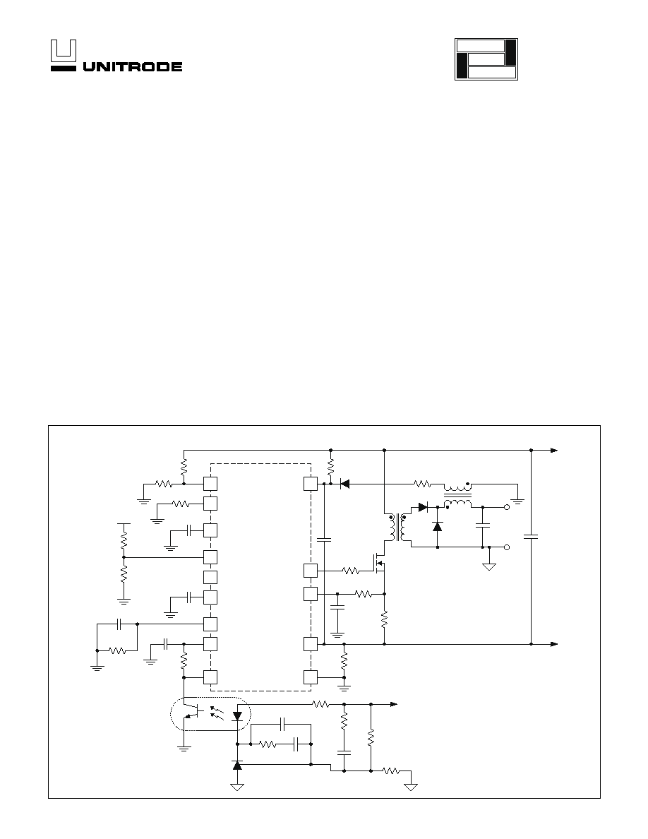
The UCC35701/UCC35702 family of pulse width modulators is intended for
isolated switching power supplies using primary side control. They can be
used for both off-line applications and DC/DC converter designs such as in
a distributed power system architecture or as a telecom power source.
The devices feature low startup current, allowing for efficient off-line start-
ing, yet have sufficient output drive to switch power MOSFETs in excess of
500kHz.
Voltage feed forward compensation is operational over a 5:1 input range
and provides fast and accurate response to input voltage changes over a
4:1 range. An accurate volt-second clamp and maximum duty cycle limit
are also featured.
Fault protection is provided by pulse by pulse current limiting as well as the
ability to latch off after a programmable number of repetitive faults has oc-
curred.
Two UVLO options are offered. UCC35701 family has turn-on and turn-off
thresholds of 13V/9V and UCC35702 family has thresholds of 9.6V/8.8V.
The UCC35701/2 and the UCC25701/2 are offered in the 14 pin SOIC (D),
14 pin PDIP (N) or in 14 pin TSSOP (PW) packages. The UCC15701/2 is
offered in the 14 pin CDIP (J) package.
3
VDD
12
VREF
8
FB
4
OUT
2
ILIM
5
PGND
C3
1
COUNT
C
F
14
SS
C
S
11
SYNC
9
VSCLAMP
VREF
10
CT
C
T
7
RT
6
VFF
13
GND
V
IN
SUPPLY
V
IN
RETURN
RGND
R10
RCS
R8
R7
R6
C2
R8
R
F
R5
R4
R3
R2
R1
V
OUT
UCC35701
C1
C4
C6
R12
C6
C5
R11
R13
C7
R14
V
OUT
R15
TYPICAL APPLICATION DIAGRAM
SLUS293A - JANUARY 2000
FEATURES
∑
700kHz Operation
∑
Integrated Oscillator/ Voltage Feed
Forward Compensation
∑
Accurate Duty Cycle Limit
∑
Accurate Volt-second Clamp
∑
Optocoupler Interface
∑
Fault Counting Shutdown
∑
Fault Latch off or Automatic Shutdown
∑
Soft Stop Optimized for Synchronous
Rectification
∑
1A Peak Gate Drive Output
∑
130
µ
A Start-up Current
∑
750
µ
A Operating Current
UDG-98005-1
application
INFO
available
2
UCC15701/2
UCC25701/2
UCC35701/2
ABSOLUTE MAXIMUM RATINGS
Supply voltage (Supply current limited to 20mA) . . . . . . . . 15V
Supply Current. . . . . . . . . . . . . . . . . . . . . . . . . . . . . . . . . 20mA
Input pins ( ILIM,VFF,RT,CT,VSCLAMP,SYNC,SS) . . . . . . 6V
Output Current (OUT) DC. . . . . . . . . . . . . . . . . . . . . +/≠180mA
Output Current (OUT) Pulse (0.5ms) . . . . . . . . . . . . . . +/≠1.2A
Storage Temperature. . . . . . . . . . . . . . . . . . . ≠65∞C to +150∞C
Junction Temperature . . . . . . . . . . . . . . . . . . . ≠55∞C to +150∞C
Lead Temperature (Soldering, 10 sec.) . . . . . . . . . . . . +300∞C
Note: All voltages are with respect to GND. Currents are posi-
tive into the specified terminal. Consult Packaging Section of
the Databook for thermal limitations and considerations of
packages.
VREF
GND
SS
SYNC
CT
FB
VSCLAMP
1
2
3
4
5
6
7
14
13
12
11
10
9
8
ILIM
COUNT
VFF
RT
VDD
OUT
PGND
CONNECTION DIAGRAMS
DIL-14, SOIC-14, TSSOP-14 (TOP VIEW)
N or J, D, PW PACKAGE
ELECTRICAL CHARACTERISTICS:
Unless otherwise specified, V
DD
= 11V, RT = 60.4k, C
T
= 330pF, C
REF
= C
VDD
=
0.1 F, V
FF
= 2.0V, and no load on the outputs.
PARAMETER
TEST CONDITIONS
MIN
TYP
MAX
UNITS
UVLO Section
Start Threshold
(UCCX5701)
12
13
14
V
(UCCX5702)
8.8
9.6
10.4
V
Stop Threshold
(UCCX5701)
8
9
10
V
(UCCX5702)
8.0
8.8
9.6
V
Hysteresis
(UCCX5701)
3
4
V
(UCCX5702)
0.3
0.8
V
Supply Current
Start-up Current
(UCCX5701) V
DD
= 11V, V
DD
Comparator Off
130
200
µ
A
(UCCX5702) V
DD
= 8V, V
DD
Comparator Off
120
190
A
I
DD
Active
V
DD
Comparator On
0.75
1.5
mA
V
DD
Clamp Voltage
(UCCX5701) I
DD
= 10mA
13.5
14.3
15
V
(UCCX5702) I
DD
= 10mA
13
13.8
15
V
V
DD
Clamp ≠ Start Threshold
(UCCX5701)
1.3
V
(UCCX5702)
4.2
V
Voltage Reference
V
REF
V
DD
= 10V to 13V, I
VREF
= 0mA to 2mA
4.9
5
5.1
V
Line Regulation
V
DD
= 10V to 13V
20
mV
Load Regulation
I
VREF
= 0mA to 2mA
2
mV
Short Circuit Current
V
REF
= 0V, T
J
= 25∞C
20
50
mA
T
A
= T
J
UVLO
Option
Package
Part Number
≠55∞C to +125∞C
13V / 9V
CDIP-14
UCC15701J
9.6V / 8.8V
CDIP-14
UCC15702J
≠40∞C to +85∞C
13V / 9V
SOIC-14
UCC25701D
PDIP-14
UCC25701N
TSSOP-14 UCC25701PW
9.6V / 8.8V
SOIC-14
UCC25702D
PDIP-14
UCC25702N
TSSOP-14 UCC25702PW
0∞C to +70∞C
13V / 9V
SOIC-14
UCC35701D
PDIP-14
UCC35701N
TSSOP-14 UCC35701PW
9.6V / 8.8V
SOIC-14
UCC35702D
PDIP-14
UCC35702N
TSSOP-14 UCC35702PW
The D and PW packages are available taped and reeled. Add
TR suffix to the device type (e.g., UCC35701DTR).
ORDERING INFORMATION
3
UCC15701/2
UCC25701/2
UCC35701/2
ELECTRICAL CHARACTERISTICS:
Unless otherwise specified, V
DD
= 11V, RT = 60.4k, C
T
= 330pF, C
REF
= C
VDD
=
0.1 F, V
FF
= 2.0V, and no load on the outputs.
PARAMETER
TEST CONDITIONS
MIN
TYP
MAX
UNITS
Line Sense
Vth High Line Comparator
3.9
4
4.1
V
Vth Low Line Comparator
0.5
0.6
0.7
V
Input Bias Current
≠100
100
nA
Oscillator Section
Frequency
V
FF
= 0.8V to 3.2V
90
100
110
kHz
Frequency
V
FF
= 0.6V to 3.4V (Note 1)
90
100
110
kHz
SYNC VIH
2
V
SYNC VIL
0.8
V
SYNC Input Current
VSYNC = 2.0V
3
10
µ
A
RT Voltage
VFF = 0.4V
0.5
0.6
0.7
V
VFF = 0.8V
0.75
0.8
0.85
V
VFF = 2.0V
1.95
2.0
2.05
V
VFF = 3.2V
3.15
3.2
3.25
V
VFF = 3.6V
3.3
3.4
3.5
V
C
T
Peak Voltage
VFF = 0.8V (Note 1)
0.8
V
VFF = 3.2V (Note 1)
3.2
V
C
T
Valley Voltage
(Note 1)
0
V
Soft Start/Shutdown/Duty Cycle Control Section
I
SS
Charging Current
10
18
30
A
I
SS
Discharging Current
300
500
750
µ
A
Saturation
V
DD
= 11V, IC Off
25
100
mV
Fault Counter Section
Threshold Voltage
VFF = 0.8V to 3.2V
3.8
4
4.2
V
Saturation Voltage
VFF = 0.8V to 3.2V
100
mV
Count Charging Current
10
18
30
µ
A
Current Limit Section
Input Bias Current
≠100
0
100
nA
Current Limit Threshold
180
200
220
mV
Shutdown Threshold
500
600
700
mV
Pulse Width Modulator Section
FB Pin Input Impedance
VFB = 3V
30
50
100
k
Minimum Duty Cycle
VFB <= 1V
0
%
Maximum Duty Cycle
VFB >= 4.5V, VSCLAMP >= 2.0V
95
99
100
%
PWM Gain
VFF = 0.8V
35
50
70
%/V
Volt Second Clamp Section
Maximum Duty Cycle
VFF = 0.8V, VSCLAMP = 0.6V
69
74
79
%
Minimum Duty Cycle
VFF = 3.2V, VSCLAMP = 0.6V
17
19
21
%
Output Section
VOH
I
OUT
= ≠100mA, (V
DD
≠ V
OUT
)
0.4
1
V
VOL
I
OUT
= 100mA
0.4
1
V
Rise Time
C
LOAD
= 1000pF
20
100
ns
Fall Time
C
LOAD
= 1000pF
20
100
ns
Note 1: Guaranteed by design. Not 100% tested in production.

4
UCC15701/2
UCC25701/2
UCC35701/2
PIN DESCRIPTIONS
VDD: Power supply pin. A shunt regulator limits supply
voltage to 14V typical at 10mA shunt current.
PGND: Power Ground. Ground return for output driver
and currents.
GND: Analog Ground. Ground return for all other circuits.
This pin must be connected directly to PGND on the
board.
OUT: Gate drive output. Output resistance is 10
maxi-
mum.
VFF: Voltage feedforward pin. This pin connects to the
power supply input voltage through a resistive divider and
provides feedforward compensation over a 0.8V to 3.2V
range. A voltage greater than 4.0V or less than 0.6V on
this pin initiates a soft stop cycle.
RT: The voltage on this pin mirrors VFF over a 0.8V to
3.2V range. A resistor to ground sets the ramp capacitor
charge current. The resistor value should be between
20k and 200k.
CT: A capacitor to ground provides the oscillator/
feedforward sawtooth waveform. Charge current is 2
∑
I
RT
, resulting in a CT slope proportional to the input volt-
age. The ramp voltage range is GND to V
RT
.
Period and oscillator frequency is given by:
T
V
C
I
t
R
C
RT
T
RT
DISCH
T
T
=
∑
∑
+
∑
∑
2
0 5
.
F
RT CT
∑
2
8
FB
9
VSCLAMP
10
CT
3
VDD
5.0V
REF
SS
2
ILIM
1
COUNT
14
13 GND
4
OUT
5
PGND
12
VREF
0.7V
13/9V (35701)
9.6/8.8V (35702)
SSDONE
7
RT
6
VFF
11
SYNC
4.5V
4V
V
REF
0.6V
0.2V
CURRENT FAULT
CURRENT LIMIT
V
REF
0.6V
4V
2*I
RT
0.2V
3
µ
A
I
25*I
RUN
I
I
RT
PEAK
VALLEY
SHUTDOWN
LATCH
FAULT
LATCH
0.2V
VDD
HIGH LINE
LOW LINE
PWM
S
Q
R
D
S
Q
R
D
1.5R
+
R
R
Q
S
D
R
Q
S
D
SSDONE
PWM
D
Q
R
DETAILED BLOCK DIAGRAM
UDG-98004

5
UCC15701/2
UCC25701/2
UCC35701/2
(Note: Refer to the Typical Application Diagram on the first
page of this datasheet for external component names.) All the
equations given below should be considered as first order ap-
proximations with final values determined empirically for a spe-
cific application.
Power Sequencing
V
DD
is normally connected through a high impedance
(R6) to the input line, with an additional path (R7) to a
low voltage bootstrap winding on the power transformer.
VFF is connected through a divider (R1/R2) to the input
line.
For circuit activation, all of the following conditions are re-
quired:
1. VFF between 0.6V and 4.0V (operational input voltage
range).
2. VDD has been under the UVLO stop threshold to reset
the shutdown latch.
3. VDD is over the UVLO start threshold.
The circuit will start at this point. I
VDD
will increase from
the start up value of 130 A to the run value of 750 A.
The capacitor on SS is charged with a 18 A current.
When the voltage on SS is greater than 0.8V, output
pulses can begin, and supply current will increase to a
level determined by the MOSFET gate charge require-
ments to I
VDD
~ 1mA + QT
∑
fs. When the output is ac-
tive, the bootstrap winding should be sourcing the supply
current. If VDD falls below the UVLO stop threshold, the
controller will enter a shutdown sequence and turn the
controller off, returning the start sequence to the initial
condition.
VDD Clamp
An internal shunt regulator clamps VDD so the voltage
does not exceed a nominal value of 14V. If the regulator
is active, supply current must be limited to less than
20mA.
APPLICATION INFORMATION
VSCLAMP: Voltage at this pin is compared to the CT
voltage, providing a constant volt-second limit. The com-
parator output terminates the PWM pulse when the ramp
voltage exceeds VSCLAMP. The maximum on time is
given by:
t
V
CT
I
ON
VSCLAMP
RT
=
∑
∑
2
The maximum duty cycle limit is given by:
D
t
T
V
V
MAX
ON
VSCLAMP
RT
=
=
FB: Input to the PWM comparator. This pin is intended
to be driven with an optocoupler circuit. Input impedance
is 50k
.
Typical modulation range is 1.6V to 3.6V.
SYNC: Level sensitive oscillator sync input. A high level
forces the gate drive output low and resets the ramp ca-
pacitor. On-time starts at the negative edge the pulse.
There is a 3
µ
A pull down current on the pin, allowing it to
be disconnected when not used.
VREF: 5.0V trimmed reference with 2% variation over
line, load and temperature. Bypass with a minimum of
0.1
µ
F to ground.
SS: Soft Start pin. A capacitor is connected between this
pin and ground to set the start up time of the converter.
After power up (V
DD
>13V AND V
REF
>4.5V), or after a
fault condition has been cleared, the soft start capacitor
is charged to V
REF
by a nominal 18
µ
A internal current
source. While the soft start capacitor is charging, and
while V
SS
< (0.4
∑
V
FB)
, the duty cycle, and therefore the
output voltage of the converter is determined by the soft
start circuitry.
At High Line or Low Line fault conditions, the soft start
capacitor is discharged with a controlled discharge cur-
rent of about 500
µ
A. During the discharge time, the duty
cycle of the converter is gradually decreased to zero.
This soft stop feature allows the synchronous rectifiers to
gradually discharge the output LC filter. An abrupt shut
off can cause the LC filter to oscillate, producing unpre-
dictable output voltage levels.
All other fault conditions (UVLO, VREF Low, Over Cur-
rent (0.6V on ILIM) or COUNT) will cause an immediate
stop of the converter. Furthermore, both the Over Current
fault and the COUNT fault will be internally latched until
V
DD
drops below 9V or V
FF
goes below the 600mV
threshold at the input of the Low Line comparator.
After all fault conditions are cleared and the soft start ca-
pacitor is discharged below 200 mV, a soft start cycle will
be initiated to restart the converter.
ILIM: Provides a pulse by pulse current limit by terminat-
ing the PWM pulse when the input is above 200mV. An
input over 600mV initiates a latched soft stop cycle.
COUNT: Capacitor to ground integrates current pulses
generated when ILIM exceeds 200mV.
A resistor to
ground sets the discharge time constant. A voltage over
4V will initiate a latched soft stop cycle.
PIN DESCRIPTIONS (cont.)

6
UCC15701/2
UCC25701/2
UCC35701/2
Output Inhibit
During normal operation, OUT is driven high at the start
of a clock period and is driven low by voltages on CT, FB
or VSCLAMP.
The following conditions cause the output to be immedi-
ately driven low until a clock period starts where none of
the conditions are true:
1. I
LIM
> 0.2V
2. FB or SS is less than 0.8V
Current Limiting
ILIM is monitored by two internal comparators. The cur-
rent limit comparator threshold is 0.2V. If the current limit
comparator is triggered, OUT is immediately driven low
and held low for the remainder of the clock cycle, provid-
ing pulse-by-pulse over-current control for excessive
loads. This comparator also causes C
F
to be charged for
the remainder of the clock cycle.
If repetitive cycles are terminated by the current limit
comparator causing COUNT to rise above 4V, the shut-
down latch is set. The COUNT integration delay feature
will be bypassed by the shutdown comparator which has
a 0.6V threshold. The shutdown comparator immediately
sets the shutdown latch. R
F
in parallel with C
F
resets the
COUNT integrator following transient faults. R
F
must be
greater than (4
∑
R4)
∑
(1 ≠ D
MAX
).
Latched Shutdown
If ILIM rises above 0.6V, or COUNT rises to 4V, the shut-
down latch will be set. This will force OUT low, discharge
SS and COUNT, and reduce I
DD
to approximately 750 A.
When, and if, V
DD
falls below the UVLO stop threshold,
the shutdown latch will reset and I
DD
will fall to 130 A,
allowing the circuit to restart. If V
DD
remains above the
UVLO stop threshold (within the UVLO band), an alter-
nate restart will occur if VFF is momentarily reduced be-
low 1V. External shutdown commands from any source
may be added into either the COUNT or ILIM pins.
Voltage Feedforward
The voltage slope on CT is proportional to line voltage
over a 4:1 range and equals 2
∑
VFF
/
(RT
∑
CT). The capaci-
tor charging current is set by the voltage across R
T
.
V(RT) tracks VFF over a range of 0.8V to 3.2V. A chang-
ing line voltage will immediately change the slope of
V(CT), changing the pulse width in a proportional man-
ner without using the feedback loop, providing excellent
dynamic line regulation.
VFF is intended to operate accurately over a 4:1 range
between 0.8V and 3.2V. Voltages at VFF below 0.6V or
above 4.0V will initiate a soft stop cycle and a chip re-
start when the under/over voltage condition is removed.
Volt-Second Clamp
A constant volt-second clamp is formed by comparing
the timing capacitor ramp voltage to a fixed voltage de-
rived from the reference. Resistors R4 and R5 set the
volt-second limit. For a volt-second product defined as
VIN
∑
t
ON(max)
, the required voltage at VSCLAMP is:
(
)
(
)
R
R
R
V
t
R
C
IN
ON
T
T
2
1
2
+
∑
∑
∑
max
.
The duty cycle limit is then:
V
V
VSCLAMP
VFF
, or
V
V
R
R
R
VSCLAMP
IN
∑
+
2
1
2
.
The
maximum
duty
cycle
is
realized
when
the
feedforward voltage is set at the low end of the operating
range (V
FF
= 0.8V).
The absolute maximum duty cycle is:
D
V
V
R
R
R
MAX
VSCLAMP
REF
=
=
∑
+
0 8
0 8
5
4
5
.
.
Frequency Set
The frequency is set by a resistor from RT to ground and
a capacitor from CT to ground. The frequency is approxi-
mately:
F
R
C
T
T
=
∑
2
(
)
External synchronization is via the SYNC pin. The pin
has a 1.5V threshold , making it compatible with 5V and
3.3V CMOS logic. The input is level sensitive, with a high
input forcing the oscillator ramp low and the output low.
An active pull down on the SYNC pin allows it to be un-
connected when not used.
Gate Drive Output
The UCC35701/2 is capable of a 1A peak output current.
Bypass with at least 0.1 F directly to PGND. The capaci-
tor must have a low equivalent series resistance and in-
ductance. The connection from OUT to the power
MOSFET gate should have a 2
or greater damping re-
sistor and the distance between chip and MOSFET
should be minimized. A low impedance path must be es-
tablished between the MOSFET source (or ground side
of the current sense resistor), the V
DD
capacitor and
PGND. PGND should then be connected by a single path
(shown as RGND) to GND.
APPLICATION INFORMATION (cont.)
7
UCC15701/2
UCC25701/2
UCC35701/2
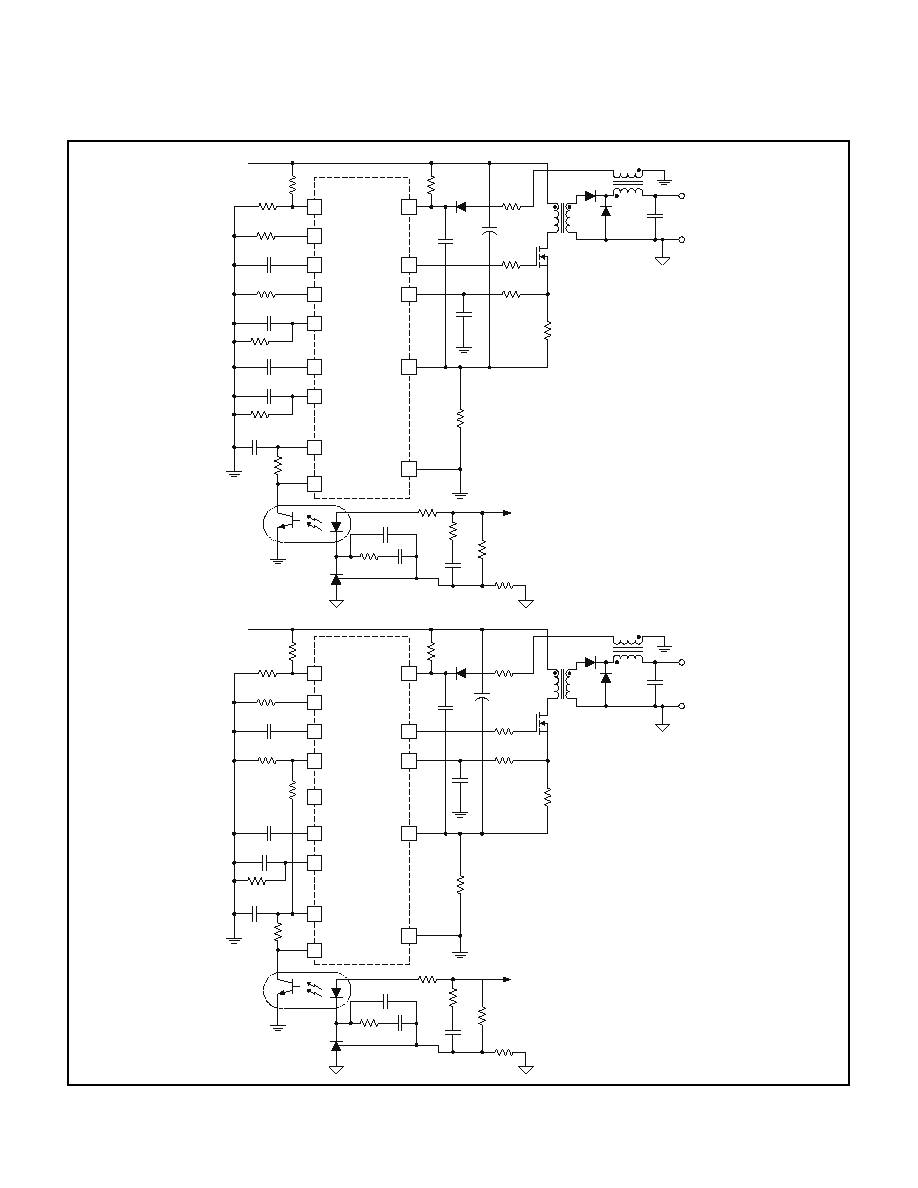
Transitioning From UCC3570 To UCC35701
The UCC35701/2 is an advanced version of the popular,
low power UCC3570 PWM.
Significant improvements
were made to the IC's oscillator and PWM control sec-
tions to enhance overall system performance. All of the
key attributes and functional blocks of the UCC3570 were
maintained in the UCC35701/2. A typical application us-
ing UCC3570 and UCC35701/2 is shown in Fig. 6 for
comparison.
The advantages of the UCC35701/2 over the UCC3570
are as follows.
∑
Improved oscillator and PWM control section.
∑
A precise maximum volt-second clamp circuit. The
UCC3570 has a dual time base between oscillator and
feedforward circuitry. The integated time base in
UCC35701/2 improves the duty cycle clamp accuracy,
providing better than
±
5% accurate volt- second
clamp over full temperature range.
∑
Separately programmable oscillator timing resistor
(RT) and capacitor (CT) circuits provide a higher
degree of versatility.
∑
An independent SYNC input pin for simple external
synchronization.
∑
A smaller value filter capacitor (0.1 F) can be used
with the enhanced reference voltage.
UCC35701/2 is pin to pin compatible to UCC3570 but is
not a direct drop-in replacement for UCC3570 sockets.
The changes required to the power supply printed circuit
board of for existing UCC3570 designs are minimal. For
conversion, only one extra resistor to set the volt-second
clamp needs to be added to the existing PC board lay-
outs. In addition, some component values will need to be
changed due to the functionality change in of four of the
IC pins.
The Pinout Changes from UCC3570 are as follows.
∑
Pin 7 was changed from SLOPE to RT (for timing
resistor)
∑
Pin 8 was changed from ISET to VSCLAMP (requiring
one additional resistor from pin 9 to VREF)
∑
Pin 10 was changed from RAMP to CT (single timing
capacitor)
∑
Pin 11 was changed from FREQ to SYNC (input only)
Additional Information
Please refer to the following two Unitrode application
topics on UCC3570 for additional information.
[1] Application Note U-150,
Applying the UCC3570 Volt-
age-Mode PWM Controller to Both Off-line and DC/DC
Converter Designs by Robert A. Mammano
[2] Design Note DN-62,
Switching Power Supply Topol-
ogy,
Voltage
Mode
vs. Current
Mode
by
Robert
Mammano
APPLICATION INFORMATION (cont.)
VSCLAMP
CT
FEEDBK
SOFT START
HIGH DC
LOW DC
ZERO DC
SOFTST
V-S CLAMP
SOFT STOP
Figure 1. Timing diagram for PWM action with forward, soft start and volt-second clamp.
TYPICAL WAVEFORMS
UDG-98207

8
UCC15701/2
UCC25701/2
UCC35701/2
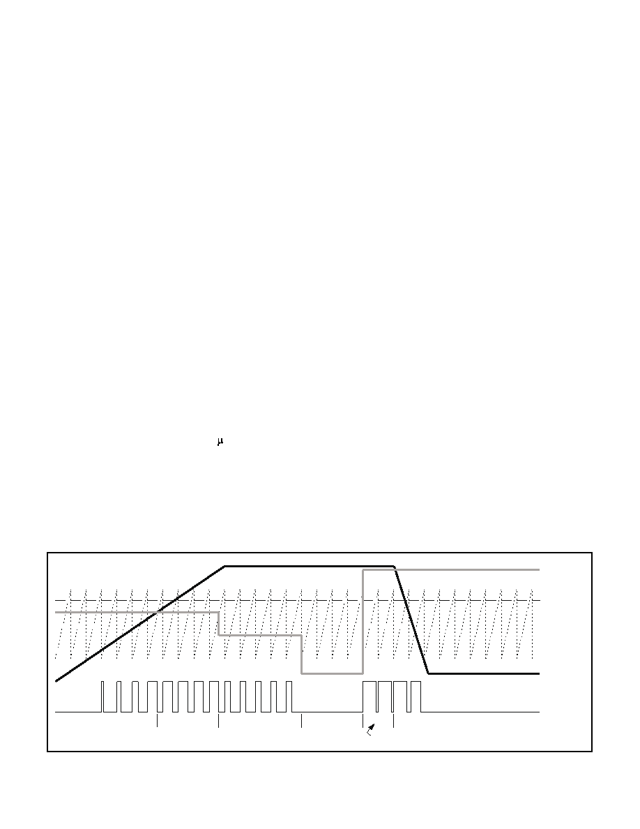
VFF
CT
SYNC
Figure 2. Timing diagram for oscillator waveforms showing feedforward action and synchronization.
TYPICAL WAVEFORMS (cont.)
10
100
1000
20
60
100
140
180
220
RT [K
]
FREQ
UENCY
[kHz]
100pF
150pF
220pF
330pF
470pF
Figure 3. Oscillator frequency vs. RT and CT.
TYPICAL CHARACTERISTIC CURVES
0.97
0.98
0.99
1.00
1.01
1.02
1.03
-55
-35
-15
5
25
45
65
85
105
125
TEMPERATURE [∞C]
NORMALIZED
DUTY
CYCLE
VFF=0.8
VFF=3.2
Figure 5. Normalized maximum duty cycle vs.
temperature.
UDG-98208
Figure 4. Oscillator frequency vs. temperature.
9
UCC15701/2
UCC25701/2
UCC35701/2
UNITRODE CORPORATION
7 CONTINENTAL BLVD. ∑ MERRIMACK, NH 03054
TEL. (603) 424-2410 ∑ FAX (603) 424-3460
6
7
10
9
11
14
1
12
8
13
3
4
2
5
VFF
SLOPE
RAMP
ISET
FREQ
SS
COUNT
VREF
FB
GND
PGND
OUT
VDD
ILIM
R5
C1
C2
R8
R
GND
R
SNS
R9
C4
R6
R7
C3
R1
R2
R3
R4
C
R
C
T
R
T
C
F
R
F
C
SS
UCC3570
V
IN+
6
7
10
9
11
14
1
12
8
13
3
4
2
5
VFF
RT
CT
VSCLAMP
SYNC
SS
COUNT
VREF
FB
GND
PGND
OUT
VDD
ILIM
R5
C1
C2
R8
R
GND
R9
R7
C3
R1
R2
R3
R4
C
T
R
NEW
C
F
R
F
C
SS
UCC35701
V
IN+
R12
C6
C5
R11
R13
C7
R14
V
OUT
R12
C6
C5
R11
R13
C7
R14
V
OUT
V
OUT
R
SNS
V
OUT
R6
C4
R15
R15
Figure 6. Single-ended forward circuit comparison between UCC3750 and UCC37501.
APPLICATION INFORMATION (cont.)
UDG-98210

IMPORTANT NOTICE
Texas Instruments and its subsidiaries (TI) reserve the right to make changes to their products or to discontinue
any product or service without notice, and advise customers to obtain the latest version of relevant information
to verify, before placing orders, that information being relied on is current and complete. All products are sold
subject to the terms and conditions of sale supplied at the time of order acknowledgment, including those
pertaining to warranty, patent infringement, and limitation of liability.
TI warrants performance of its semiconductor products to the specifications applicable at the time of sale in
accordance with TI's standard warranty. Testing and other quality control techniques are utilized to the extent
TI deems necessary to support this warranty. Specific testing of all parameters of each device is not necessarily
performed, except those mandated by government requirements.
Customers are responsible for their applications using TI components.
In order to minimize risks associated with the customer's applications, adequate design and operating
safeguards must be provided by the customer to minimize inherent or procedural hazards.
TI assumes no liability for applications assistance or customer product design. TI does not warrant or represent
that any license, either express or implied, is granted under any patent right, copyright, mask work right, or other
intellectual property right of TI covering or relating to any combination, machine, or process in which such
semiconductor products or services might be or are used. TI's publication of information regarding any third
party's products or services does not constitute TI's approval, warranty or endorsement thereof.
Copyright
©
2000, Texas Instruments Incorporated