UCC1581
UCC2581
UCC3581
MARCH 1999 - REVISED MARCH 2003 - SLUS295B
FEATURES
∑
Low 85
µ
A Startup Current
∑
Low 300
µ
A Operating Current
∑
Automatically Disabled
Startup Preregulator
∑
Programmable Minimum Duty
Cycle with Cycle Skipping
∑
Programmable Maximum
Duty Cycle
∑
Output Current 1A Peak
Source and Sink
∑
Programmable Soft Start
∑
Programmable Oscillator
Frequency
∑
External Oscillator
Synchronization Capability
Micropower Voltage Mode PWM
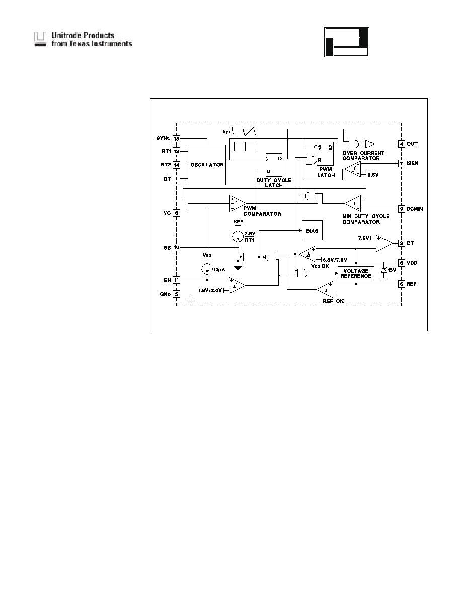
BLOCK DIAGRAM
DESCRIPTION
The UCC3581 voltage mode pulse width modulator is de-
signed to control low power isolated DC - DC converters
in applications such as Subscriber Line Power (ISDN
I.430). Primarily used for single switch forward and
flyback converters, the UCC3581 features BiCMOS cir-
cuitry for low startup and operating current, while main-
taining
the
ability
to
drive
power
MOSFETs
at
frequencies up to 100kHz. The UCC3581 oscillator al-
lows the flexibility to program both the frequency and the
maximum duty cycle with two resistors and a capacitor. A
TTL level input is also provided to allow synchronization
to an external frequency source.
The UCC3581 includes programmable soft start circuitry,
overcurrent detection, a 7.5V linear preregulator to con-
trol chip V
DD
during startup, and an on-board 4.0V logic
supply.
The UCC3581 provides functions to maximize light load
efficiency that are not normally found in PWM controllers.
A linear preregulator driver in conjunction with an exter-
nal depletion mode N-MOSFET provides initial controller
power. Once the bootstrap supply is functional, the
preregulator is shut down to conserve power. During light
load, power is saved by providing a programmable mini-
mum duty cycle clamp. When a duty cycle below the
minimum is called for, the modulator skips cycles to pro-
vide the correct average duty cycle required for output
regulation. This effectively reduces the switching fre-
quency, saving significant gate drive and power stage
losses.
The UCC3581 is available in 14-pin plastic and ceramic
dual-in-line packages and in a 14-pin narrow body small
outline IC package (SOIC). The UCC1581 is specified for
operation from
-
55
∞
C to +125
∞
C, the UCC2581 is speci-
fied for operation from
-
40
∞
C to +85
∞
C, and the
UCC3581 is specified for operation from 0
∞
C to +70
∞
C.
Note: Pin Connection shown for 14-pin Package
UDG-95011-1
application
INFO
available
2
UCC1581
UCC2581
UCC3581
Supply Voltage (I
DD
10mA). . . . . . . . . . . . . . . . . . . . . . . . 15V
Supply Current . . . . . . . . . . . . . . . . . . . . . . . . . . . . . . . . . 30mA
V
REF
Current . . . . . . . . . . . . . . . . . . . . . . . . . . . . . . . . . . ≠10mA
OUT Current . . . . . . . . . . . . . . . . . . . . . . . . . . . . . . . . . . . .
±
1A
Analog Inputs
EN . . . . . . . . . . . . . . . . . . . . . . . . . . . . ≠0.3V to (VDD + 0.3V)
VC, ISEN, SYNC, DCMIN. . . . . . . . . . ≠0.3V to (V
REF
+ 0.3V)
Power Dissipation at T
D
= 25∞C
(N, J, Q, L Package) . . . . . . . . . . . . . . . . . . . . . . . . . . . . . 1W
(D Package) . . . . . . . . . . . . . . . . . . . . . . . . . . . . . . . . . 0.65W
Storage Temperature . . . . . . . . . . . . . . . . . . . ≠65∞C to +150∞C
Junction Temperature . . . . . . . . . . . . . . . . . . . ≠55C to +150∞C
Lead Temperature (Soldering, 10 sec.) . . . . . . . . . . . . . +300∞C
Unless otherwise specified, all voltages are with respect to
Ground. Currents positive into, negative out of the specified ter-
minal. Consult Packaging Section of Databook for thermal limi-
tations and considerations of packages.
ABSOLUTE MAXIMUM RATINGS
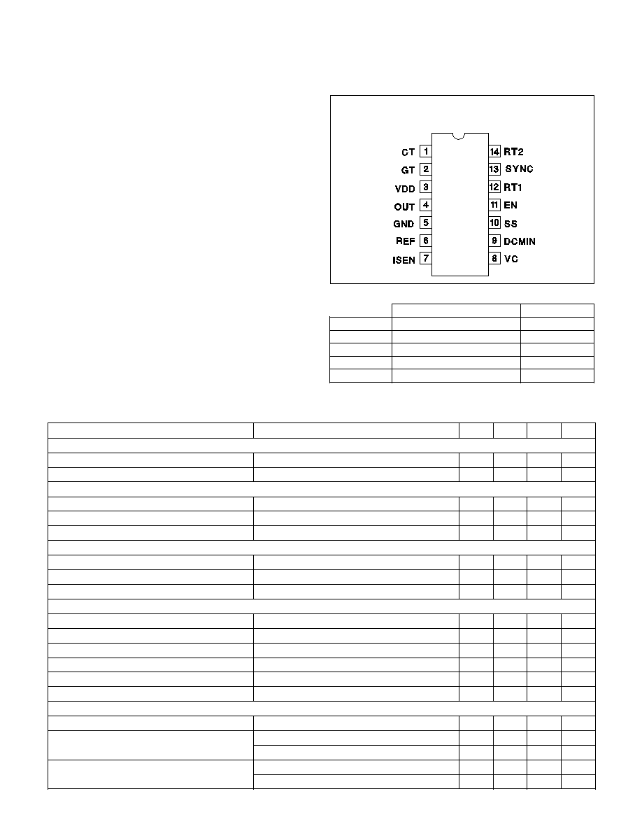
CONNECTION DIAGRAMS
DIL-14, SOIC-14 (Top View)
N or J, D Packages
ELECTRICAL CHARACTERISTICS:
Unless otherwise stated, these specifications apply for VDD = 10V, 0.1
µ
F capacitor
from VDD to GND, 1.0
µ
F capacitor from REF to GND, RT1 = 680k
, RT2 = 12k
, CT = 750pF and T
A
= T
J
.
PARAMETER
TEST CONDITIONS
MIN
TYP
MAX
UNITS
Reference Section
Output Voltage
I = ≠0.2mA
3.94
4.0
4.06
V
Load Regulation
≠5.0mA < I < ≠0.2mA
20
45
mV
Undervoltage Lockout Section
Start Threshold
6.7
7.3
7.9
V
Minimum Operating Voltage After Start
6.2
6.8
7.4
V
Hysteresis
0.2
0.5
0.8
V
Linear Preregulator Section
Regulated VDD Voltage
7.0
7.5
8.0
V
Regulated VDD to UVLO Delta
100
230
600
mV
VDD Override Threshold
8.2
V
Oscillator Section
Frequency
25∞C
18
19.5
21
kHz
Temperature Stability
(Note 1)
3.0
%
CT Peak Voltage
(Note 1)
2.5
V
CT Valley Voltage
(Note 1)
1.0
V
SYNC VIH
1.9
2.1
2.3
V
SYNC VIL
(Note 1)
1.8
V
PWM SECTION
Maximum Duty Cycle
81
84
87
%
Minimum Duty Cycle
(VC < 1.0V) DCMIN = 0V
0
%
(VC > 1.0V at start of cycle) DCMIN = 1.18V
7
10
13
%
Input Bias Current
(DCMIN), (Note 1)
≠150
20
150
nA
(VC), (Note 1)
≠150
20
150
nA
TEMPERATURE RANGE
PACKAGE
UCC1581J
≠55∞C to +125∞C
CDIP
UCC2581D
≠40∞C to +85∞C
SOIC
UCC2581N
≠40∞C to +85∞C
PDIP
UCC3581D
0∞C to +70∞C
SOIC
UCC3581N
0∞C to +70∞C
PDIP
ORDERING INFORMATION
3
UCC1581
UCC2581
UCC3581
ELECTRICAL CHARACTERISTICS:
Unless otherwise stated, these specifications apply for VDD = 10V, 0.1
µ
F capacitor
from VDD to GND, 1.0
µ
F capacitor from REF to GND, RT1 = 680k
, RT2 = 12k
, CT = 750pF and T
A
= T
J
.
PARAMETER
TEST CONDITIONS
MIN
TYP
MAX
UNITS
Current Sense Section
Input Bias Current
≠150
20
150
nA
Overcurrent Threshold
0.4
0.5
0.6
V
Output Section
OUT Low Level
I = 100mA
0.6
1.2
V
OUT High Level
I = ≠100mA, VDD ≠ OUT
0.6
1.2
V
Rise/Fall Time
(Note 1)
20
100
ns
Soft start Section
Soft start Current
SS = 2V
≠9
≠11.5
≠14
µ
A
Chip Enable Section
VIH
1.9
2.0
2.1
V
VIL
1.7
1.8
1.9
V
Hysteresis
180
230
280
mV
Source Current
5
10
15
µ
A
Overall Section
Start-Up Current
VDD < Start Threshold
85
130
µ
A
Operating Supply Current
VC = 0V
300
600
µ
A
VDD Zener Shunt Voltage
I
DD
= 10mA
13.5
15
16.5
V
I
DD
Stand-by Shunt Voltage
EN = 0V
100
150
µ
A
Note 1: Guaranteed by design. Not 100% tested in production
CT: Oscillator timing capacitor pin. Minimum value is
100pF.
DCMIN: Input for programming minimum duty cycle
where pulse skipping begins. This pin can be grounded
to disable minimum duty cycle feature and pulse
skipping.
EN: Enable input. This pin has an internal 10
µ
A pull-up.
A logic low input inhibits the PWM output and causes the
soft start capacitor to be discharged.
GND: Circuit ground.
GT: Pin for controlling the gate of an external depletion
mode N-MOSFET for the startup supply. The external
N-MOSFET regulates VDD to 7.5V until the bootstrap
supply comes up, then GT goes low.
ISEN: Input for overcurrent comparator. This function can
be used for pulse-by-pulse current limiting. The threshold
is 0.5V nominal.
OUT: Gate drive output to external N-MOSFET.
REF: 4.0V reference output. A minimum value bypass
capacitor of 1.0
µ
F is required for stability.
RT1: Resistor pin to program oscillator charging current.
The oscillator charging current is 9 2
2 0
1
.
.
∑
V
RT
.
See Application Diagram Fig. 1.
The current into this pin is
2 0
1
.
V
RT
.
The value of RT1 should be between 220k and 1M
.
RT2: Resistor pin to program oscillator discharge time.
The minimum value of RT2 is 10k
. See Application
Diagram Fig. 1.
SS: Soft start capacitor pin. The charging current out of
SS is 3.75X the current in RT1.
SYNC: Oscillator synchronization pin. Rising edge
triggered CMOS/TTL compatible input with a 2.1V
threshold. SYNC should be grounded if not used. The
minimum pulse width of the SYNC signal is 100ns.
VC: Control voltage input to PWM comparator. The
nominal control range of VC is 1.0V to 2.5V.
VDD: Chip input power with an 15V internal clamp. VDD
is regulated by startup FET to 7.5V until the bootstrap
voltage comes up. VDD should be bypassed at the chip
with a 0.1
µ
F minimum capacitor.
PIN DESCRIPTIONS
4
UCC1581
UCC2581
UCC3581
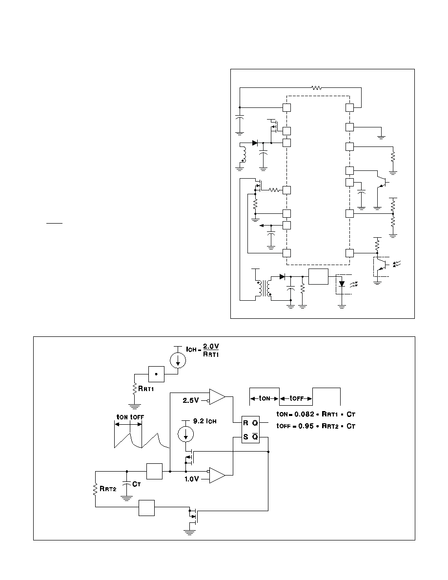
The UCC3581's oscillator allows the user the flexibility to
program the frequency and the duty cycle by adjusting
two resistors and a capacitor. Application Diagram Fig. 1
shows these components as RT1, RT2, and C
T
. RT1 pro-
grams the timing capacitor charging current which results
in a linear ramp charging C
T
. Discharge of C
T
is accom-
plished though RT2 which results in a standard RC dis-
charge waveform. The oscillator on-time (C
T
charging) is
calculated by the formula
t
RT
C
ON
T
=
∑
∑
0 082
1
.
.
The off-time (C
T
discharging) is calculated by the formula
t
RT
C
OFF
T
=
∑
∑
0 95
1
.
.
Resistor RT1 programs the charging current. The current
is:
2.0V
RT
1
.
CT charging current is 9.2 times the current in RT1. RT1
can range from 220k
to 1M
. Minimum capacitor size
is 100pF, and minimum RT2 size is 10k.
A Block Diagram of the Oscillator is shown in Fig. 2. The
oscillator also has an external synchronization pin.
When a low to high level is detected, and if the oscilla-
tor's output is in the high state (C
T
charging), the oscilla-
tor
output
immediately
goes
low
and
C
T
starts
discharging. The sync input is rising edge sensitive and
is ignored when the oscillator output is low.
APPLICATION INFORMATION
1
3
2
14
C
T
RT2
V
IN
1
µ
F
D2
4
Q1
5
6
1
µ
F
7
T1
R
L
REF &
E/A
U1
CT
GT
VDD
OUT
GND
REF
ISEN
V
IN
8
VC
9
DCMIN
10
SS
11
EN
U1
REF
REF
C
SS
12
RT1
13
SYNC
RT2
RT1
REF
UCC3581
D1
BSS129 OR
EQUIV.
Figure 1. Application diagram.
UDG-99043
Figure 2. Oscillator.
UDG-96105

5
UCC1581
UCC2581
UCC3581
The externally bypassed 4.0V reference is controlled by
undervoltage lockout and chip enable circuitry. The en-
able input is internally tied to a 10
µ
A current source
which allows the pin to be driven by an open collector
driver. The part is also enabled if EN floats. The
UCC3581 has a soft start function which requires a user
supplied external timing capacitor. When in soft start
mode, the soft start capacitor, C
SS
, is charged with a
constant current source. The soft start current is 3.75X
the current in RT1.
There is an on-chip control amplifier, which when driving
the gate of an external depletion mode N-MOSFET, acts
as a 7.5V linear preregulator supplying VDD directly from
the primary input power line. The preregulator may sub-
sequently be fully disabled by a tertiary bootstrap winding
providing a minimum of 8.2V to the VDD pin.
Computation of DCMIN
DCMIN for a given duty cycle is calculated as follows:
(
)
V
i
DC
t
t
C
OSC
ON
OFF
T
=
∑
∑
+
where:
∑
i = oscillator charge current = 9.2 . (2.0V/RT1)
∑
DC = Duty Cycle, as a fraction of 1
∑
t
ON
= 0.082
∑
RT1
∑
CT
∑
t
OFF
= 0.95
∑
RT2
∑
CT
∑
C
T
= Oscillator Capacitor
The CT pin ramp slews from 1V to 2.5V. Therefore, add
V to 1V to get DCMIN voltage.
Example: For 10% duty cycle with RT1 = 680k
, RT2 =
12k
, and CT = 705pF,
(
)
V
i
DC
t
t
C
OSC
ON
OFF
T
=
∑
∑
+
( )
=
∑
∑
∑
∑
+
∑
-
-
9 2
2 0
680
0 1
4 182 10
8 55 10
5
6
.
.
.
.
sec
.
sec
V
k
750 10
12
∑
-
V
V
=
0 18
.
Therefore,
DCMIN
V
V
V
=
+
=
1
0 18
1 18
.
.
A Typical Micropower Application
The circuit shown in Fig. 3 illustrates the use of the
UCC3581 in a micropower application. The isolated 5V
flyback power supply uses a minimum of parts and oper-
ates over an 8:1 input voltage range (15VDC to 120VDC)
while delivering a regulated 5V output with a load swing
from 0W to 1W. It operates in the discontinuous mode at
light load or high line, and continuous mode at heavier
loads and lower line voltages. Higher input line voltages
are possible by simply increasing the voltage ratings of
C1, Q1, D1 and D2.
The most notable feature of the design is its efficiency.
With a load of 1 watt, the typical efficiency is 82%, drop-
ping to 70% around 50mW. With a load of only 12.5mW,
the efficiency remains as high as 50%. At this load, with
an input of 50V, the total input current is only 500
µ
A.
Note that the power supply can be disabled by pulling the
UCC3581 enable pin low, in which case the input current
drops to less than 150
µ
A.
The UCC3581 achieves very low losses by means of low
quiescent current and pulse skipping at light loads which
reduces switching losses. The degree of pulse skipping is
controlled by programming the minimum duty cycle. In
this example, the frequency is 35kHz at maximum load
and drops to <2kHz at 12.5mW load (minimum pulse
width of around 6
µ
sec, or 21% duty cycle at 35kHz).
Another way losses are reduced is operating with a VDD
of around 10V rather than the more common 12V to 16V.
At such light primary currents, the MOSFET remains in
full saturation with a gate drive voltage well below 10V.
Gate drive losses are minimized by choosing a MOSFET
with low total gate charge, in this case only 8nC maxi-
mum. By choosing a large gate drive resistor, EMI is min-
imized by reducing peak currents. Due to pulse skipping,
switching times are less critical for efficiency at light load.
The
shunt
regulator
(LM3411)
and
optocoupler
(MOC8100) are also key to the efficiency at such light
loads, and were chosen for their low operating current.
The LM3411 has a quiescent current of only 150
µ
A max-
imum (compared to 1mA for the more common TL431).
In addition, because it is not a three terminal device, the
LM3411's quiescent current does not flow in the
optocoupler LED. Since this bias current is not in the
feedback control path, a higher value pull-up resistor can
be used on the optocoupler output transistor, further re-
ducing losses.
APPLICATION INFORMATION (cont.)

6
UCC1581
UCC2581
UCC3581
Figure 3. Micropower power supply with 50% efficiency at 12.5mW load.
TYPICAL APPLICATION
UDG-96104
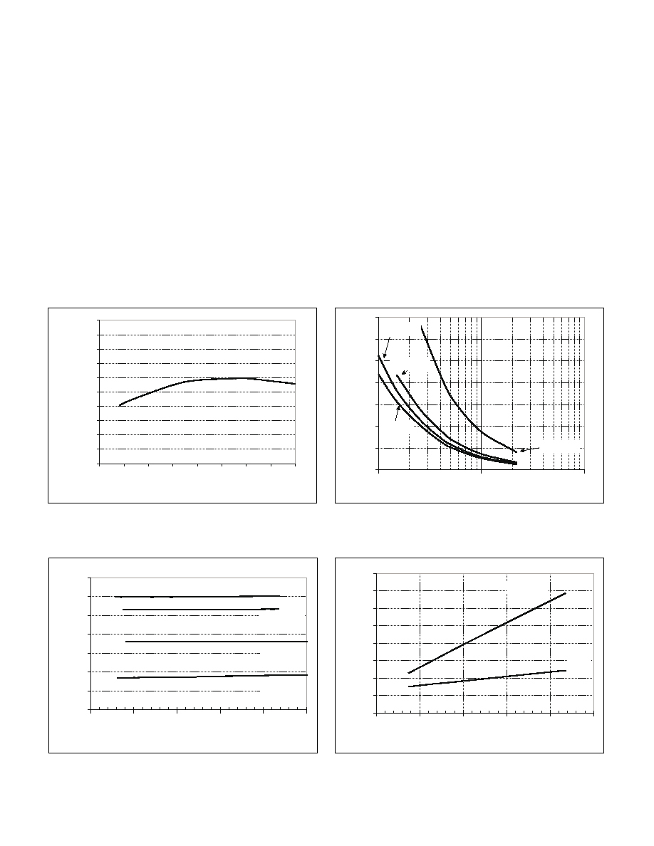
0
10
20
30
40
50
60
70
80
90
10
100
1000
Output Load [mW]
Ef
f
i
ciency
[
%
]
100V Line
25V Line
Figure 4. UCC3581 efficiency vs. line and load.
7
UCC1581
UCC2581
UCC3581
A rather large soft start capacitor was chosen to give a
startup time of several hundred milliseconds, reducing
the input surge current while the output is coming up.
Note that for stability, the UCC3581 V
REF
bypass capaci-
tor needs to be at least 1
µ
F. The V
DD
supply also needs
some capacitance to hold it up between pulses at light
load and high line, where the frequency may drop to less
than 1kHz due to pulse skipping. Otherwise it may drop
low enough for the startup MOSFET to be biased on,
lowering efficiency.
If the sync input is used, it should not be left in a high im-
pedance state where noise could cause false triggering.
If unused, it should be grounded.
The transformer was designed with a standard Magnetics
RM8 ferrite core using P material, gapped for an A
L
of
1600mH/1000Turn
2
. The primary consists of 44 turns,
while the 5V secondary has 10 turns and the bootstrap
winding 18 turns. For simplicity, all the windings can be
#28 AWG. A two section bobbin was used to provide high
primary to secondary isolation. A much smaller design,
with reduced isolation, could have been done for this low
power level.
APPLICATION INFORMATION (cont.)
3.90
3.92
3.94
3.96
3.98
4.00
4.02
4.04
4.06
4.08
4.10
-75
-50
-25
0
25
50
75
100 125
TEMPERATURE [∞C]
VREF
[V]
Figure 5. Reference voltage vs. temperature.
TYPICAL CHARACTERISTIC CURVES
0
20
40
60
80
100
120
140
100
1000
10000
CT [pF]
FREQ
UENCY
[kHz]
1M/10k
470k/47k
680k/12k
220k/10k
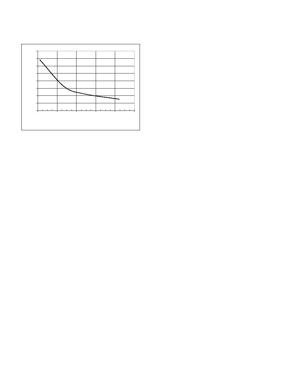
Figure 6. Frequency vs. CT vs. RT1 and RT2.
0
200
400
600
800
1000
1200
1400
1600
0
20
40
60
80
100
FREQUENCY [kHz]
I
DD
[uA]
1nF LOAD
NO
LOAD
Figure 8. I
DD
vs. frequency RT1 = 680k, RT2 = 12k.
30
40
50
60
70
80
90
100
0
20
40
60
80
100
FREQUENCY [kHz]
DUTY
CYCLE
[
%]
220K/10K
680K/12K
470K/47K
1M/10K
Figure 7. Duty cycle vs. frequency vs. RT1 / RT2.
8
UCC1581
UCC2581
UCC3581
UNITRODE CORPORATION
7 CONTINENTAL BLVD. ∑ MERRIMACK, NH 03054
TEL. (603) 424-2410
FAX (603) 424-3460
0
5
10
15
20
25
30
35
40
200
400
600
800
1000
1200
RT1 [kW]
I
SO
FT
ST
AR
T
[uA]
Figure 9. Soft start current vs. RT1.
TYPICAL CHARACTERISTIC CURVES (cont.)

IMPORTANT NOTICE
Texas Instruments Incorporated and its subsidiaries (TI) reserve the right to make corrections, modifications,
enhancements, improvements, and other changes to its products and services at any time and to discontinue
any product or service without notice. Customers should obtain the latest relevant information before placing
orders and should verify that such information is current and complete. All products are sold subject to TI's terms
and conditions of sale supplied at the time of order acknowledgment.
TI warrants performance of its hardware products to the specifications applicable at the time of sale in
accordance with TI's standard warranty. Testing and other quality control techniques are used to the extent TI
deems necessary to support this warranty. Except where mandated by government requirements, testing of all
parameters of each product is not necessarily performed.
TI assumes no liability for applications assistance or customer product design. Customers are responsible for
their products and applications using TI components. To minimize the risks associated with customer products
and applications, customers should provide adequate design and operating safeguards.
TI does not warrant or represent that any license, either express or implied, is granted under any TI patent right,
copyright, mask work right, or other TI intellectual property right relating to any combination, machine, or process
in which TI products or services are used. Information published by TI regarding third≠party products or services
does not constitute a license from TI to use such products or services or a warranty or endorsement thereof.
Use of such information may require a license from a third party under the patents or other intellectual property
of the third party, or a license from TI under the patents or other intellectual property of TI.
Reproduction of information in TI data books or data sheets is permissible only if reproduction is without
alteration and is accompanied by all associated warranties, conditions, limitations, and notices. Reproduction
of this information with alteration is an unfair and deceptive business practice. TI is not responsible or liable for
such altered documentation.
Resale of TI products or services with statements different from or beyond the parameters stated by TI for that
product or service voids all express and any implied warranties for the associated TI product or service and
is an unfair and deceptive business practice. TI is not responsible or liable for any such statements.
Mailing Address:
Texas Instruments
Post Office Box 655303
Dallas, Texas 75265
Copyright
2003, Texas Instruments Incorporated