11/98
FEATURES
∑
Precision Secondary Side Post
Regulation for Multiple Output Power
Supplies
∑
Useful for Both Single Ended and
Center Tapped Secondary Circuits
∑
Ideal Replacement for Complex
Magnetic Amplifier Regulated Circuits
∑
Leading Edge Modulation
∑
Does Not Require Gate Drive
Transformer
∑
High Frequency (>500kHz) Operation
∑
Applicable for Wide Range of Output
Voltages
∑
High Current Gate Driver (0.5A
Sink/1.5A Source)
∑
Average Current Limiting Loop
DESCRIPTION
The UCC3583 is a synchronizable secondary side post regulator for preci-
sion regulation of the auxiliary outputs of multiple output power supplies. It
contains a leading edge pulse width modulator, which generates the gate
drive signal for a FET power switch connected in series with the rectifying
diode. The turn-on of the power switch is delayed from the leading edge of
the secondary power pulse to regulate the output voltage. The UCC3583
contains a ramp generator slaved to the secondary power pulse, a voltage
error amplifier, a current error amplifier, a PWM comparator and associ-
ated logic, a gate driver, a precision reference, and protection circuitry.
The ramp discharge and termination of the gate drive signal are triggered
by the synchronization pulse, typically derived from the falling edge of the
transformer secondary voltage. The ramp starts charging again once its
low threshold is reached. The gate drive signal is turned on when the ramp
voltage exceeds the control voltage. This leading edge modulation tech-
nique prevents instability when the UCC3583 is used in peak current mode
primary controlled systems.
The controller operates from a floating power supply referenced to the out-
put voltage being controlled. It features an undervoltage lockout (UVLO)
circuit, a soft start circuit, and an averaging current limit amplifier. The cur-
rent limit can be programmed to be proportional to the output voltage, thus
achieving foldback operation to minimize the dissipation under short circuit
conditions.
(continued)
UCC1583
UCC2583
UCC3583
Switch Mode Secondary Side Post Regulator
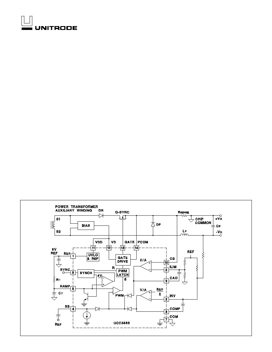
TYPICAL APPLICATION AND BLOCK DIAGRAM
UDG-96201-2
Note: Pin connections shown for 14-pin packages.
2
UCC1583
UCC2583
UCC3583
ABSOLUTE MAXIMUM RATINGS
V
DD
. . . . . . . . . . . . . . . . . . . . . . . . . . . . . . . . . . . . . . . . . . 15V
I
VDD
. . . . . . . . . . . . . . . . . . . . . . . . . . . . . . . . . . . . . . . . . 15mA
RAMP . . . . . . . . . . . . . . . . . . . . . . . . . . . . . ≠0.3V to V
DD
+ 1V
I
RAMP
. . . . . . . . . . . . . . . . . . . . . . . . . . . . . . . . . . . . . . . . . 5mA
I
REF . . . . . . . . . . . . . . . . . . . . . . . . . . . . . . . . . . . . . . . . . . . . . . . . . . . .
≠30mA
P
COM
. . . . . . . . . . . . . . . . . . . . . . . . . . . . . . . . . . ≠0.2V to 0.2V
I
GATE
(twp < 1
µ
S and Duty Cycle < 10%) . . . . . . ≠0.8A to 1.8A
I
COMP
. . . . . . . . . . . . . . . . . . . . . . . . . . . . . . . . . . ≠5mA to 5mA
I
CAO
. . . . . . . . . . . . . . . . . . . . . . . . . . . . . . . . . . . ≠5mA to 5mA
V
SYNC
. . . . . . . . . . . . . . . . . . . . . . . . . . . . ≠0.6V to V
REF
+0.3V
I
SYNC
. . . . . . . . . . . . . . . . . . . . . . . . . . . . . . . . . ≠05mA to 5mA
INV, SS, ILIM, ISENSE. . . . . . . . . . . . . . ≠0.3V to VREF + 0.3V
Storage Temperature . . . . . . . . . . . . . . . . . . . ≠65∞C to +150∞C
Junction Temperature . . . . . . . . . . . . . . . . . . . ≠55∞C to +150∞C
Lead Temperature (Soldering, 10 sec.) . . . . . . . . . . . . . +300∞C
All voltages are with respect to the COM terminal unless other-
wise stated. Currents are positive into, negative out of the
specified terminal. Consult Packaging Section of Databook for
thermal limitations and considerations of packages.
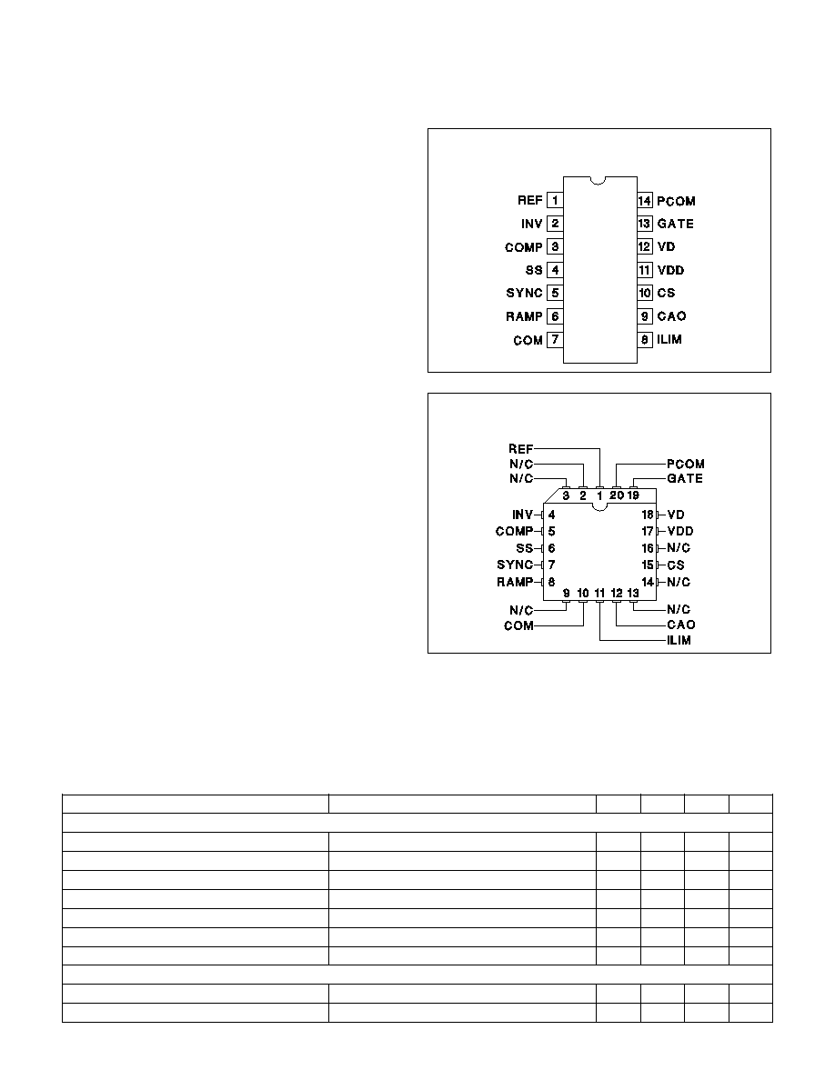
CONNECTION DIAGRAMS
DIL-14, SOIC-14 (Top View)
J, N, or D Packages
ELECTRICAL CHARACTERISTICS:
Unless otherwise stated, these specifications apply for T
A
= ≠55
∞
C to 125
∞
C for
UCC1583, ≠40∞C to 85∞C for UCC2583, and 0∞C to 70∞C for UCC3583; VDD = 12V, R
T
= 60k, C
T
= 200pF, T
A
= T
J
.
PARAMETER
TEST CONDITIONS
MIN
TYP
MAX
UNITS
Ramp Generation and Synchronization
Maximum Input Operating Frequency
For input with 5% to 90% duty cycle (Note 1)
500
kHz
Ramp Frequency, Free Running
95
100
105
kHz
Ramp Discharge Current
V
RAMP
= 0.5V
2.0
3.6
mA
Low Threshold Voltage
No min, no max, 0=TYP
0
V
High Threshold Voltage
3.75
4
4.25
V
Synchronizing Threshold Voltage (On)
(Note 1)
1
V
Synchronizing Comparator Hysteresis
1
V
Output Duty Cycle
Minimum Duty Cycle
Output D/C = Output PW / Input PW
0
%
Maximum Duty Cycle
Output D/C = Output PW / Input PW
100
%
PLCC-20 (Top View)
Q Package
3
UCC1583
UCC2583
UCC3583
ELECTRICAL CHARACTERISTICS:
Unless otherwise stated, these specifications apply for T
A
= ≠55
∞
C to 125
∞
C for
UCC1583, ≠40∞C to 85∞C for UCC2583, and 0∞C to 70∞C for UCC3583; VDD = 12V, R
T
= 60k, C
T
= 200pF, T
A
= T
J
.
PARAMETER
TEST CONDITIONS
MIN
TYP
MAX
UNITS
Voltage Error Amplifier
V
INV
V
COMP
= V
INV
, 0∞C to 70∞C (UCC3583)
2.462
2.5
2.538
V
V
COMP
= V
INV
, All Other Temperature Ranges
2.45
2.5
2.55
V
I
INV
V
COMP
= V
INV
300
500
nA
V
COMP
Low
V
INV
= 2.6V, I
COMP
= 100
µ
A
450
700
mV
V
COMP
High
V
INV
= 2.4V, I
COMP
= ≠100
µ
A
5.0
5.5
6.0
V
AVOL
No Load
70
90
dB
GBW Product
At f = 100kHz, T
A
= 25∞C (Note 1)
3
5
MHz
Current Error Amplifier
Input Offset Voltage
10
mV
Input CM Low
Common Mode for CS and ILIM (Note 1)
0
V
Input CM High
Common Mode for CS and ILIM (Note 1)
2
V
V
CAO
Low
V
+IN
= 0V, V
≠IN
= 0.1V, I
CAO
= 100
µ
A
250
500
mV
V
CAO
High
V
+IN
= 0V, V
≠IN
= 0.1V, I
CAO
= ≠100
µ
A
5.0
5.5
6.0
V
Input Current (ILIM and CS Pins)
≠50
0
50
nA
AVOL
No Load
70
90
dB
GBW Product
At f = 100kHz, T
A
= 25∞C
2
4
MHz
Soft Start Current
10
25
µ
A
UVLO
VDD On Threshold Voltage
8.5
9.0
9.5
V
VDD Off Threshold Voltage
7.9
8.4
8.9
V
UVLO Hysteresis
0.3
0.6
0.9
V
Bias Supply
Supply Clamp Voltage
13
14
15
V
Supply Current (VDD)
f = 100kHz With No Gate Output Load
3
5
mA
Output Driver
V
SAT
High
I
GATE
= ≠150mA
0.6
1.0
V
V
SAT
Low
I
GATE
= 50mA
0.4
0.75
V
Rise Time
C
GATE
= 1nF
50
75
ns
Fall Time
C
GATE
= 330pF
20
40
ns
Reference
V
REF
I
REF
= 0, 0∞C to 70∞C (UCC3583)
4.925
5
5.075
V
I
REF
= 0, All Other Temperature Ranges
4.900
5
5.100
V
Line Regulation
VDD = 10V to 14V
2
30
mV
Load Regulation
I
REF
= 0mA to 2mA
1
20
mV
Note 1: Guaranteed by design. Not 100% tested in production.

4
UCC1583
UCC2583
UCC3583
Power Stage Circuit Configuration
The UCC3583 is designed for use in a post regulator ap-
plication for tightly regulating auxiliary outputs in a multi-
ple output converter. The post regulation is applied to the
secondary side power pulse of a power transformer
where the power pulse is controlled by the feedback sig-
nal from the main output. In order to simplify the applica-
tion of the UCC3583, it is required that the IC be
referenced to the positive output terminal and the output
filter inductor be placed in the return path. The place-
ment of the inductor in the return path facilitates better
EMI performance, in addition to making magnetic de-
signs and terminations easier to implement. Typical set-
up and circuit waveforms of the UCC3583 system appli-
cation are shown in Figure 1. Figure 2 shows waveforms
for a single ended output rectifier application of the
UCC3583 shown on page 1. The UCC3583 can also be
used in half bridge rectifier applications as shown by the
circuit and waveforms depicted in Figures 3 and 4. Refer-
encing the IC to the positive output terminal creates a re-
quirement for a floating bias voltage for the IC which can
be referenced to the same positive voltage terminal. Pos-
sible implementations of deriving the floating bias voltage
are shown in Figure 5.
APPLICATION INFORMATION
CAO: Output of the current error amplifier. Averaging of
the sensed current signal is provided by connecting an
integrating capacitor between ILIM and CAO. CAO feeds
into the PWM comparator input and controls the loop
when its voltage is higher than the voltage at COMP
(output of the voltage error amplifier).
COM: Signal ground for the chip. It is connected to the
positive terminal of the output voltage being regulated by
the IC.
COMP: Output of the voltage error amplifier fed into the
PWM comparator. Loop compensation components are
connected between COMP and INV.
CS: Non-inverting input of the current error amplifier. The
sensed current signal from the current sense resistor is
connected to this pin. By making the signal at CS
proportional to the output voltage, effective current
foldback limiting can be provided.
GATE: Gate drive output for the power switch FET. The
drive pin has a 0.5A sink/1.5A source capability and very
low output off-state impedance.
ILIM: Inverting input of the current error amplifier. It sets
the DC limit for the output current.
INV: Inverting input of the voltage error amplifier. The
feedback signal is connected to this pin using a resistive
divider between REF and ≠V
O
.
PCOM: Power ground for the chip. It is connected to the
source terminal of the MOSFET being regulated by the
IC.
RAMP: This pin is the input to the PWM comparator and
provides a ramp signal for generation of the PWM signal.
A capacitor to COM and a resistor to REF set the
charging rate for the ramp. An internal current source of
1mA discharges RAMP when synchronization signal
appears or when RAMP crosses a 4V threshold. In the
intended mode of operation, the switching frequency is
determined by the secondary power pulse. The RC
components at RAMP should be selected to give an
appropriately sized ramp signal. In the absence of a
synchronizing pulse, these RC components determine
the free running frequency of the controller.
REF: Precision 5V reference pin. REF stays off until
VDD exceeds 9V and turns off again when VDD drops
below 8.4V. Bypass REF to COM.
SS: This pin provides a soft start function. A capacitor to
REF programs the soft start time. During soft start, the
PWM comparator is controlled by the soft start voltage
resulting in a slow increase in output duty cycle. Once
the soft start capacitor is discharged, output control is
dictated by the larger of the output at CAO or COMP.
SYNC: Synchronization input pin. It is connected to a
signal representative of the secondary power pulse. One
possible implementation is to use a resistive divider
between terminal S2 of the secondary winding shown in
Figure 1 and REF for generating the input to the SYNC
pin. The synchronizing comparator is referenced to 0.5V
and has
±
500mV of hysteresis. The trip levels are
approximate 1.0V and 0.0V. The designer should prevent
the SYNC pin from exceeding 0.3V below ground as this
will turn on the ESD diode.
VD: Power supply for the output driver. VD should be
tied to VDD in the application.
VDD: Power supply for the chip. VDD should be
bypassed to COM. VDD has to be 9V for the IC to start
and 8.4V for it to remain operational. A shunt clamp from
VDD to COM limits the supply voltage to 14V.
PIN DESCRIPTIONS

5
UCC1583
UCC2583
UCC3583
For the circuit shown in Figure 5a, CC1 is charged when
the transformer voltage is positive and the synchronous
switch is on. During the off period of Q-SYNC, the charge
is transferred to CC2 through diode DC2. Diode DC3
charges CC2 during the blocking interval of Q-SYNC.
This method is preferable when the transformer positive
voltage is high enough to generate the required bias volt-
age. For the circuit shown in Figure 5b, CC1 is charged
during the period when reverse (reset) voltage appears
across the secondary. The charge on CC1 is transferred
to CC2 through DC2 when Q-SYNC turns on. This
method is preferable when the reverse voltage is high
enough to generate the required bias voltage. The series
resistor should be chosen to handle the required voltage
drop at full IC operating current when the zener clamp
across VDD and COM is activated.
The following is a description of the major functional
blocks of the UCC3583. Refer to Figure 6 (Typical Appli-
cation Circuit) for component designations.
UVLO and Start Up
The UCC3583 has an internal undervoltage lockout cir-
cuit which keeps the internal circuitry inactive until VDD
exceeds the upper threshold (9V). Once the chip is acti-
vated, VDD has to be above the lower UVLO threshold
(8.4V) for it to remain functional. The IC requires a low
startup current of only 100
µ
A when VDD is under the
UVLO threshold. VDD has an internal clamp of 14V
which can sink up to 10mA. Measures must be taken not
to exceed this current. The internal reference (REF) is
brought up when the UVLO on threshold is exceeded.
The soft start pin provides an effective means to start the
IC in a controlled manner. An internal current of 10
µ
A
starts discharging a capacitor connected to SS when the
UVLO conditions have been removed. The voltage on
SS controls the duty cycle of the output during the dis-
charge period.
Synchronizing Circuit and Oscillator
UCC3583 is primarily intended for synchronizable opera-
tion where its switching frequency is determined by the
secondary pulse of the power transformer. However, it
has an internal oscillator which allows it to operate in
free-running mode when an external synchronization
pulse is not available. The switching frequency is deter-
mined by resistor R
T
connected between REF and
RAMP and capacitor C
T
connected from RAMP to GND.
The frequency is given by:
CH
DIS
CH
T
T
=
+
=
∑
∑
and
(
)
(
)
DIS
T
RAMP p p
RAMP dis
T
=
∑
∑
`
The values of R
T
and C
T
are also dictated by the fact
that the ramp is discharged through an internal imped-
ance of 2k. The value of R
T
needs to be at least 50k to
ensure that the internal discharge current is the current
through R
T
during the entire discharge period. This re-
sults in making the value of C
T
relatively small for a de-
sired frequency of operation.
When the synchronizing signal is available, the oscillator
frequency should be programmed to be lower than the
synchronizing frequency to ensure proper operation. A
large difference in self-running and synchronizing fre-
quencies leads to smaller ramp amplitude and higher
noise sensitivity. The ramp capacitor is discharged when
the synchronization signal arrives and begins charging
when the low threshold is crossed.
There are two methods to synchronize to the secondary
pulse. One method is to use the rising edge of the sec-
ondary pulse, which reduces the maximum duty cycle
available. Subsequently, the post regulator switch cannot
be turned on during the C
T
discharge time. The other
method is to use the falling edge of the secondary pulse
for synchronization. This method is preferable because it
allows a slower discharge of the ramp capacitor without
affecting the maximum available duty cycle of the post
regulator. The UCC3583 SYNC input needs to reach a
fixed threshold (1.0V typical) for synchronization to take
effect. Hence the IC is usable with either method of syn-
chronization. However, the UCC3583 oscillator configu-
ration is better suited for synchronization to the falling
edge. A recommended method to implement the syn-
chronization is shown in Figure 6. By connecting SYNC
to a resistive divider between REF and the secondary
terminal S2, the synchronization is achieved whenever
the voltage on S2 goes from a negative value to zero. R
A
and R
B
should be selected so that the voltage on the
SYNC pin varies from 0V to 1V. Placement of a Schottky
diode from SYNC to COM prevents the voltage at SYNC
from going negative. The internal hysteretic SYNC com-
parator has an inverting input set to 0.5V with about
±
0.5V hysteresis.
PWM Comparator
The UCC3583 uses a leading edge PWM scheme. In a
leading edge PWM, the output pulse (gate signal) is
turned on when the error amplifier crosses the PWM
ramp and turned off by the clock/oscillator. Leading edge
modulation is naturally provided by magamp type post
regulators and is an essential feature for post regulators.
Without the leading edge modulation in a multiple output
APPLICATION INFORMATION (cont.)

6
UCC1583
UCC2583
UCC3583
converter with post regulation on one or more outputs,
the primary current shape does not remain monotonic
and can lead to instability when the primary current is
used for current mode control or current limiting. When
compared to conventional trailing edge PWMs, the lead-
ing edge modulation leads to a phase inversion that
needs to be accounted for in the feedback loop. For the
UCC3583, this inversion is automatically provided since
the sensed voltage at the power supply output negative
terminal has a negative polarity with respect to the chip
common. Thus, UCC3583 does not require inverting
buffers which would otherwise be needed.
Error Signal Generation and Current Limiting
The PWM comparator in the UCC3583 is controlled by
three parallel loops with only one of them in effect at a
time. During normal operation, the voltage error amplifier
output is fed to the PWM comparator. The voltage error
amplifier can be compensated using commonly used
feedback techniques to achieve the desired dynamic per-
formance. The ouput drive capability of the voltage am-
plifier
is
limited
to
100
µ
A,
so
appropriately
high
impedances should be used to utilize the full output
swing of the amplifier. During startup, the soft start ca-
pacitor controls the pulse width. The third control loop is
provided by the average current amplifier. By sensing the
instantaneous inductor current and filtering/averaging it
with the current error amplifier, accurate current limiting
is achieved. This loop is in effect only during the overcur-
rent mode and provides a more accurate and noise free
control of the maximum output current compared to con-
ventional peak current limiting circuits. The current limit is
set by programming the voltage at ILIM based on the
current sense resistor chosen. In addition, the current
limit can be made proportional to the output voltage in or-
der to limit the power dissipation under short circuit con-
ditions. This is implemented by inserting a bias voltage
on CS which is proportional to the output voltage.
Gate Drive Circuit
The gate drive circuit of the UCC3583 provides high cur-
rent drive capability and is very easy to implement as a
result of tying the chip common to the source of the
switching device. Turn on current is higher (1.5A) as fast
turn on is essential for low losses and effective operation.
During the turn off, the drain voltage disappears, so turn
off time can be slower without increasing switching
losses.
APPLICATION INFORMATION (cont.)
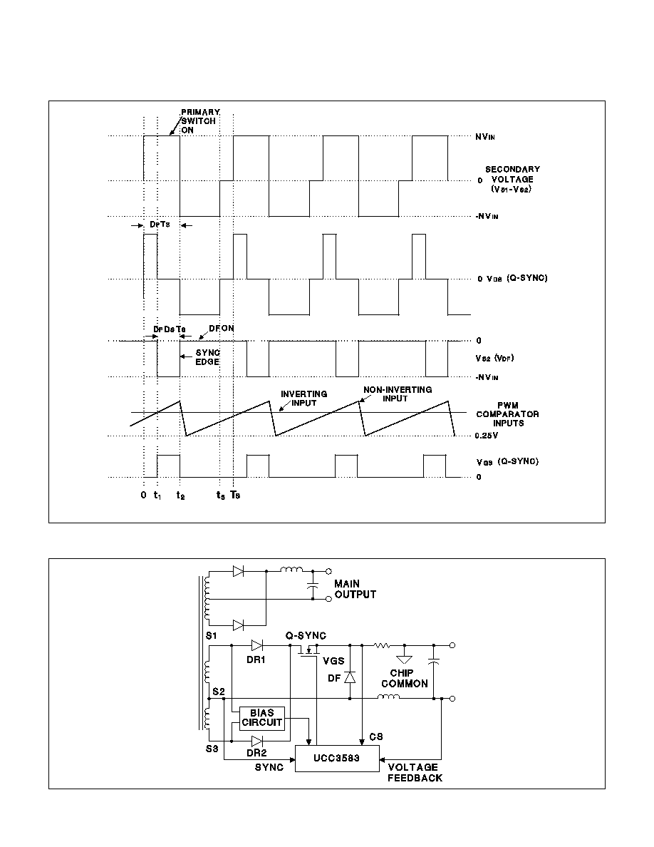
Figure 1. UCC3583 SSPR system application and typical waveforms.
UDG-98195
7
UCC1583
UCC2583
UCC3583
Figure 2. Single ended post regulator waveforms.
APPLICATION INFORMATION (cont.)
UDG-96141-1
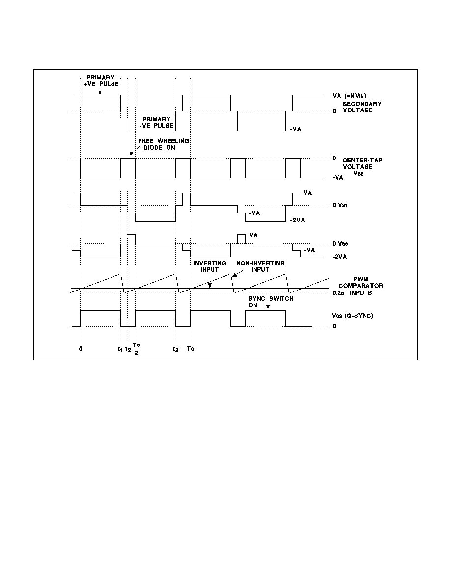
Figure 3. Half-bridge synchronous post regulator application.
UDG-96142-1
Note: All waveforms are referenced to chip common.
8
UCC1583
UCC2583
UCC3583
Figure 4. Half-bridge synchronous post regulator to waveforms.
APPLICATION INFORMATION (cont.)
UDG-96143-1

9
UCC1583
UCC2583
UCC3583
UNITRODE CORPORATION
7 CONTINENTAL BLVD. ∑ MERRIMACK, NH 03054
TEL. (603) 424-2410 ∑ FAX (603) 424-3460
APPLICATION INFORMATION (cont.)
Figure 5. Possible implementation for floating bias voltage generation.
UDG-96175-1
Figure 6. Typical application circuit.
UDG-96072-2
RA
RB

IMPORTANT NOTICE
Texas Instruments and its subsidiaries (TI) reserve the right to make changes to their products or to discontinue
any product or service without notice, and advise customers to obtain the latest version of relevant information
to verify, before placing orders, that information being relied on is current and complete. All products are sold
subject to the terms and conditions of sale supplied at the time of order acknowledgement, including those
pertaining to warranty, patent infringement, and limitation of liability.
TI warrants performance of its semiconductor products to the specifications applicable at the time of sale in
accordance with TI's standard warranty. Testing and other quality control techniques are utilized to the extent
TI deems necessary to support this warranty. Specific testing of all parameters of each device is not necessarily
performed, except those mandated by government requirements.
CERTAIN APPLICATIONS USING SEMICONDUCTOR PRODUCTS MAY INVOLVE POTENTIAL RISKS OF
DEATH, PERSONAL INJURY, OR SEVERE PROPERTY OR ENVIRONMENTAL DAMAGE ("CRITICAL
APPLICATIONS"). TI SEMICONDUCTOR PRODUCTS ARE NOT DESIGNED, AUTHORIZED, OR
WARRANTED TO BE SUITABLE FOR USE IN LIFE-SUPPORT DEVICES OR SYSTEMS OR OTHER
CRITICAL APPLICATIONS. INCLUSION OF TI PRODUCTS IN SUCH APPLICATIONS IS UNDERSTOOD TO
BE FULLY AT THE CUSTOMER'S RISK.
In order to minimize risks associated with the customer's applications, adequate design and operating
safeguards must be provided by the customer to minimize inherent or procedural hazards.
TI assumes no liability for applications assistance or customer product design. TI does not warrant or represent
that any license, either express or implied, is granted under any patent right, copyright, mask work right, or other
intellectual property right of TI covering or relating to any combination, machine, or process in which such
semiconductor products or services might be or are used. TI's publication of information regarding any third
party's products or services does not constitute TI's approval, warranty or endorsement thereof.
Copyright
©
1999, Texas Instruments Incorporated