 | –≠–ª–µ–∫—Ç—Ä–æ–Ω–Ω—ã–π –∫–æ–º–ø–æ–Ω–µ–Ω—Ç: UCC3588 | –°–∫–∞—á–∞—Ç—å:  PDF PDF  ZIP ZIP |
UCC3588
PRELIMINARY
DESCRIPTION
The UCC3588 synchronous step-down (Buck) regulator provides accurate
high efficiency power conversion. Using few external components, the
UCC1588 converts 5V to an adjustable output ranging from 3.5VDC to
2.1VDC in 100mV steps and 2.05VDC to 1.3VDC in 50mV steps with 1%
DC system accuracy. A high level of integration and novel design allow this
16-pin controller to provide a complete control solution for today's
demanding
microcontroller
power
requirements. Typical
applications
include on board or VRM based power conversion for Intel Pentium II
microprocessors,
as
well
as
other
processors
from
a
variety
of
manufacturers. High efficiency is obtained through the use of synchronous
rectification.
The softstart function provides a controlled ramp up of the system output
voltage. Overcurrent circuitry detects a hard (or soft) short on the system
output voltage and invokes a timed softstart/shutdown cycle to reduce the
PWM controller on time to 5%.
The oscillator frequency is externally programmed with RT and operates
over a range of 50kHz to 800kHz. The gate drivers are low impedance to-
tem pole output stages capable of driving large external MOSFETs. Cross
conduction is eliminated by fixed delay times between turn off and turn on
of the external high side and synchronous MOSFETs. The chip includes
undervoltage lockout circuitry which assures the correct logic states at the
outputs during power up and power down.
(continued)
5-Bit Programmable Output BiCMOS Power Supply Controller
FEATURES
∑
5-Bit Digital-to-Analog Converter
(DAC) supports Intel Pentium II
∑
Microprocessor VID Codes
∑
Compatible with 5V or 12V Systems
∑
1% Output Voltage Accuracy
Guaranteed
∑
Drives 2 N-Channel MOSFETs
∑
Programmable Frequency to 800kHz
∑
Power Good OV / UV / OVP Voltage
Monitor
∑
Undervoltage Lockout and Softstart
Functions
∑
Short Circuit Protection
∑
Low Impedance MOSFET Drivers
∑
Chip Disable
SLUS311 - JULY 1999
4
11
15
5
6
7
8
3
16
12
9
10
1
2
14
13
UCC3588
VCC
DRVHI
PWRGOOD
D0
D1
D2
D3
D4
SS/ENBL
GND
COMP
VFB
VSENSE
ISNS
DRVLO
RT
R2
47k
C5
33nF
C16
10
µ
F
R1
10K
C4
C3
C2
C1
+
+
+
+
RTN
D0
D1
D2
D3
D4
R3
200k
C6
220pF
C7 22pF
R7
15k
C13
1nF
R8
20k
R4
3
R5
3
R6
0.003
C15
150
µ
F
C12
C11
C10
C8
+
+
RTN
VOUT
L1
1.6
µ
H
Q2
IRL3103
Q1
IRL3103
D2
D1
12V IN
5V IN
C8-C12 1500
µ
F
+
+
+
C1-C4
1500
µ
F
+
C14
150
µ
F
C9
+
APPLICATION DIAGRAM
UDG-98158
2
UCC3588
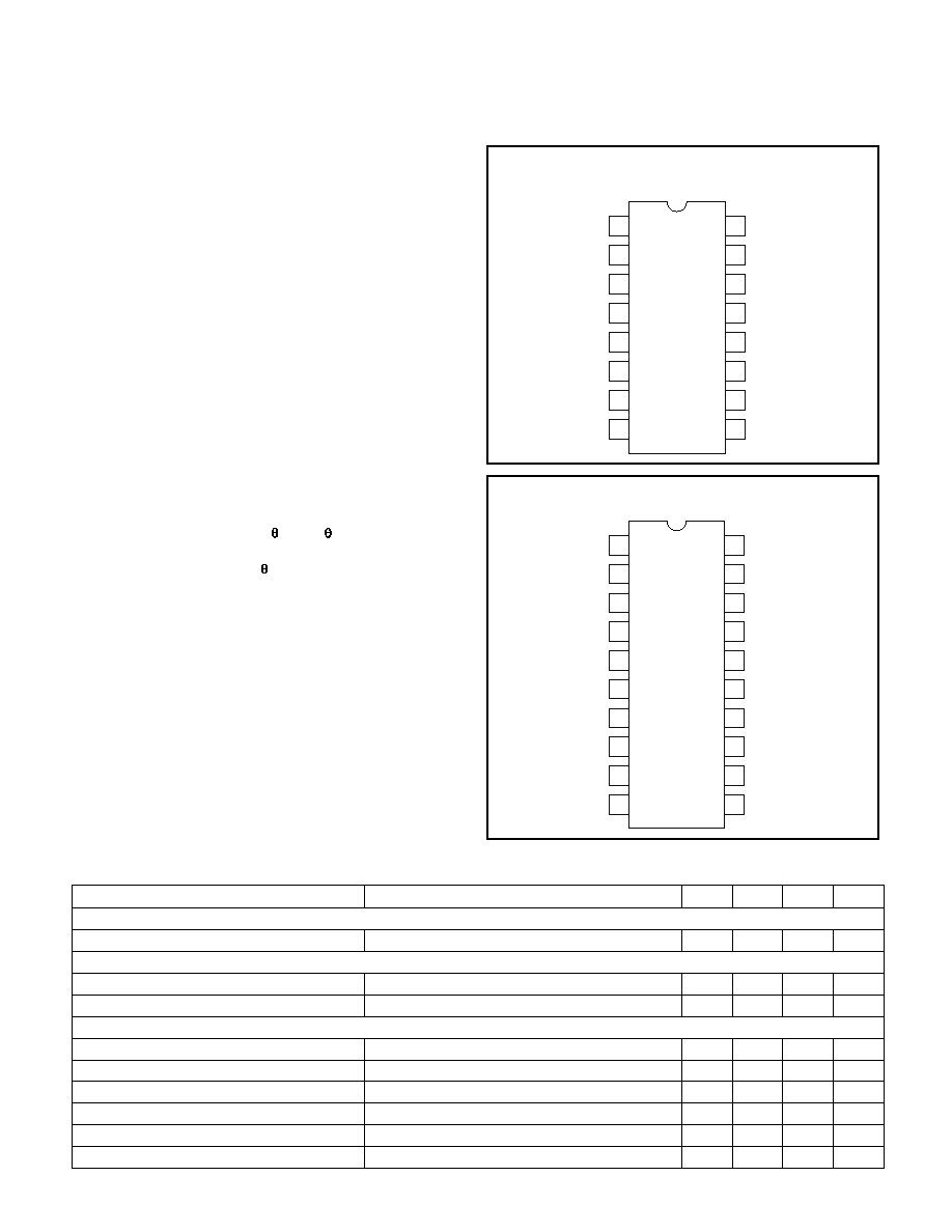
DIP-16, SOIC-16, TSSOP-16 (TOP VIEW)
N, J, D and PW Packages
ABSOLUTE MAXIMUM RATINGS
Supply Voltage V
CC
. . . . . . . . . . . . . . . . . . . . . . . . . . . . . . 15V
Gate Drive Current, 50% Duty Cycle . . . . . . . . . . . . . . . . . . 1A
Input Voltage, V
SENSE
, V
FB
, SS, COMMAND, COMP . . . . . 5V
Input Voltage, D0, D1, D2, D3, D4 . . . . . . . . . . . . . . . . . . . 6V
Input Current, RT, COMP . . . . . . . . . . . . . . . . . . . . . . . . . 5mA
Currents are positive into, negative out of the specified termi-
nal. Consult Packaging Section of Databook for thermal limita-
tions and considerations of packages. All voltages are
referenced to GND.
THERMAL DATA
Plastic DIP Package
Thermal Resistance Junction to Leads,
jc . . . . . . . . 45∞C/W
Thermal Resistance Junction to Ambient,
ja . . . . . . 90∞C/W
Ceramic DIP Package
Thermal Resistance Junction to Leads,
jc . . . . . . . . 28∞C/W
Thermal Resistance Junction to Ambient,
ja . . . . . 120∞C/W
Standard Surface Mount Package
Thermal Resistance Junction to Leads,
jc . . . . . . . . 35∞C/W
Thermal Resistance Junction to Ambient,
ja . . . . . 120∞C/W
Note: The above numbers for
ja and
jc are maximums for
the limiting thermal resistance of the package in a standard
mounting configuration. The
ja numbers are meant to be
guidelines for the thermal performance of the device and
PC-board system. All of the above numbers assume no ambi-
ent airflow, see the packaging section of Unitrode Product Data
Handbook for more details.
RT
16
15
14
13
12
11
10
9
1
2
3
4
5
6
7
8
VCC
DRVLO
DRVHI
GND
PWRGOOD
VFB
COMP
VSENSE
ISNS
SS/ENBL
D0
D1
D2
D3
D4
CONNECTION DIAGRAMS
ELECTRICAL CHARACTERISTICS:
Unless otherwise stated, these specifications hold for T
A
= 0∞C to 70∞C. T
A
= T
J
.
V
CC
= 12V, RT = 49k.
PARAMETER
TEST CONDITIONS
MIN
TYP
MAX
UNITS
Supply Current Section
Supply Current, On
V
CC
= 12V, V
RT
= 2V
4.5
5.5
mA
UVLO Section
VCC UVLO Turn-On Threshold
10.05
10.50
10.85
V
UVLO Threshold Hysteresis
350
450
550
mV
Voltage Error Amplifier Section
Input Bias Current
V
CM
= 2.0V
≠0.025 ≠0.050
µ
A
Open Loop Gain
(Note 5)
77
dB
Output Voltage High
I
COMP
= ≠500
µ
A
3.5
3.6
V
Output Voltage Low
I
COMP
= +500
µ
A
0.2
0.5
V
Output Source Current
V
VFB
= 2V, V
COMMAND
= V
COMP
= 2.5V
≠400
≠500
µ
A
Output Sink Current
V
VFB
= 3V, V
COMMAND
= V
COMP
= 2.5V
5
10
mA
This device is available in 16- pin surface mount, plastic
and ceramic DIP, TSSOP packages, and 20 pin surface
mount. The UCC3588 is specified for operation from 0∞C
to +70∞C.
DESCRIPTION (cont.)
PVCC
VCC
RT
DRVLO
DRVHI
GND
PGND
PWRGOOD
ISNS
VSENSE
N/C
D1
D2
SS/ENBL
N/C
D0
D4
D3
VFB
20
19
18
17
16
15
14
13
12
11
1
2
3
4
5
6
7
8
9
10
COMP
SOIC-20 (TOP VIEW)
DW Package
3
UCC3588
ELECTRICAL CHARACTERISTICS:
Unless otherwise stated, these specifications hold for T
A
= 0∞C to 70∞C. T
A
= T
J
.
V
CC
= 12V, RT = 49k.
PARAMETER
TEST CONDITIONS
MIN
TYP
MAX
UNITS
Oscillator/PWM Section
Initial Accuracy
0∞C <T
A
< 70∞C
250
270
290
kHz
Ramp Amplitude (p≠p)
1.85
V
Ramp Valley Voltage
0.65
V
PWM Max Duty Cycle
COMP = 3V (Note 5)
100
%
PWM Min Duty Cycle
COMP = 0. 3V (Note 5)
0
%
PWM Delay to Outputs (High to Low)
COMP = 1.5V (Note 5)
150
ns
PWM Delay to Outputs (Low to High)
COMP = 1.5V (Note 5)
150
ns
Transient Window Comparator Section
Detection Range High (Duty Cycle = 0)
% Over V
COMMAND
, (Note 1)
3
%
Detection Range Low (Duty Cycle = 1)
% Under V
COMMAND
, (Note 1)
≠3
%
Propagation Delay (V
SENSE
to Outputs)
150
200
nS
Soft Start/ Shutdown Section
SS Charge Current (Normal Start Up)
Measured on SS
≠6
≠12
µ
A
SS Charge Current (Short Circuit Fault
Condition)
Measured on SS
≠60
≠100
≠120
µ
A
SS Discharge Current (During Timeout
Sequence)
Measured on SS
1
2.5
5
µ
A
Shutdown Threshold
Measured on SS
4.1
4.2
4.3
V
Restart Threshold
Measured on SS
0.4
0.5
0.6
V
Soft Start Complete Threshold (Normal
Start-Up)
Measured on SS
3.5
3.7
3.9
V
DAC / Reference Section
COMMAND Voltage Accuracy
10.8V < V
CC
< 13.2V, measured on COMP,
0∞C < T
A
< +70∞C, (Note 2)
≠1.0
1.0
%
D0≠D4 Voltage High
5.5
6
6.5
V
D0≠D4 Voltage Threshold
2.5
3.0
3.5
V
D0≠D4 Voltage Input Bias Current
V(D4,...,D0) < 0.5V
≠80
≠100
µ
A
Overvoltage Comparator Section
Trip Point
% Over V
COMMAND
, (Note 1)
8
12
%
Hysteresis
10
20
35
mV
Undervoltage Comparator Section
Trip Point
% Under V
COMMAND
, (Note 1)
≠8.0
≠12.0
%
Hysteresis
10
20
35
mV
PWRGOOD Signal Section
Output Impedance
V
CC
= 12V, I
PWRGOOD
= 1mA
470
Overvoltage Protection Section
Trip Point
% Over V
COMMAND
, (Note 1)
15
17.5
20
%
Hysteresis
20
35
mV
VSENSE Input Bias Current
OV, OVP, UV Combined
≠8
≠12
≠16
µ
A
4
UCC3588
ELECTRICAL CHARACTERISTICS:
Unless otherwise stated, these specifications hold for T
A
= 0∞C to 70∞C. T
A
= T
J
.
V
CC
= 12V, RT = 49k.
PARAMETER
TEST CONDITIONS
MIN
TYP
MAX
UNITS
Gate Drivers (DRVHI, DRVLO) Section
Output High Voltage
I
GATE
= 100mA, V
CC
= 12V
10.8
11.5
V
Output Low Voltage
I
GATE
=≠ 100mA, V
CC
= 12V
0.5
0.8
V
Driver Non-overlap Time
(DRVHI≠ to DRVLO+)
(Note 3)
90
120
150
ns
Driver Non-overlap Time
(DRVLO≠ to DRVHI+)
(Note 3)
50
80
120
ns
Driver Rise Time
3nF Capacitive Load
80
100
ns
Driver Fall Time
3nF Capacitive Load
80
100
ns
Current Limit Section
Start of Quick Charge to Shutdown
Threshold
V
ISNS
= V
SENSE
+ 75mV, C
SS
= 10nF, (Note 4)
(Note 5)
50
µ
s
Current Limit Threshold Voltage
V
THRESHOLD
= V
ISNS
≠ V
VSENSE
40
54
70
mV
ISNS Input Bias Current
≠8
≠12
≠16
µ
A
Note 1: This percentage is measured with respect to the ideal command voltage programmed by the V
ID
(D0,....,D4) pins and ap-
plies to all DAC codes from 1.3 to 3.5V.
Note 2: Reference and error amplifier offset trimmed while the voltage amp is set in unity gain mode.
Note 3: Deadtime delay is measured from the 50% point of DRVHI falling to the 50% point of DRVLO rising, and vice-verse.
Note 4: This time is dependent on the value of C
SS
.
Note 5: Guaranteed by design. Not 100% tested in production.
10
8
7
6
5
4
3
DAC
OVP
OV/UV
+
≠
9
1
SOFTSTART
CURRENT
LIMIT
BLOCK
OVER-
CURRENT
2
11
OSC
16
R
S
Q
VREF
15
12
TURN
ON
DELAY
TURN
ON
DELAY
ANTI CROSS-
CONDUCTION
13
14
V
CC
UVLO
10.5V
VBIAS
VOLTAGE
AMPLIFIER
COMP
VFB
D4
D3
D2
D1
D0
SS/ENBL
ISNS
VSENSE
PWRGOOD
RT
GND
VCC
DRVHI
DRVLO
COMMAND
≠3%
COMMAND
+3%
VSENSE
DUTY=1
DUTY=0
SHUTDOWN
PWM
COMP.
COMMAND
SHUTDOWN
TO
VREF
SHUTDOWN
+
+
≠
+
≠
BLOCK DIAGRAM
UDG-98152

5
UCC3588
COMP: (Voltage Amplifier Output) The system voltage
compensation network is applied between COMP and
VFB.
D0, D1, D2, D3, D4: These are the digital input control
codes for the DAC. The DAC is comprised of two ranges
set by D4, with D0 representing the least significant bit
(LSB) and D3, the most significant bit (MSB). A bit is set
low by being connected the pin to GND; a bit is set high
by floating the pin. Each control pin is pulled up to ap-
proximately 6V by an internal pull-up. If one of the low
voltage codes is commanded on the DAC inputs, the out-
puts will be disabled. The outputs will also be disabled for
all 1's, the NO CPU command.
DRVHI: (PWM Output, MOSFET Driver) This output pro-
vides a low Impedance totem pole driver. Use a series
resistor between this pin and the gate of the external
MOSFET to prevent excessive overshoot. Minimize cir-
cuit trace length to prevent DRVHI from ringing below
GND.
DRVHI is disabled during UVLO conditions.
DRVHI has a typical output impedance of 5
for a V
CC
voltage of 12V.
DRVLO: (synchronous rectifier output, MOSFET driver)
This output provides a low Impedance totem pole driver
to drive the low-side synchronous external MOSFET.
Use a series resistor between this pin and the gate of the
external MOSFET to prevent excessive overshoot. Mini-
mize circuit trace length to prevent DRVLO from ringing
below GND. DRVLO is disabled during UVLO conditions.
DRVLO has a typical output impedance of 5
for a V
CC
voltage of 12V.
GND: (Ground) All voltages measured with respect to
ground. Vcc should be bypassed directly to GND with a
0.1µF or larger ceramic capacitor. The timing capacitor
discharge current also returns to this pin, so the lead
from the oscillator timing to GND should be as short and
direct as possible.
ISNS:
(Current Limit Sense Input)
A resistance con-
nected between this sense connection and Vsense sets
up the current limit threshold (54mV typical voltage
threshold).
PWRGOOD: This pin is an open drain output which is
driven low to reset the microprocessor when VSNS rises
above or falls below its nominal value by 8.5%(typ). The
on resistance of the open-drain switch is no higher than
470
. This output should be pulled up to a logic level
voltage and should be programmed to sink 1mA or less.
RT: (Oscillator Charging Current) This pin is a low im-
pedance voltage source set at ~1.25V. A resistor from
RT to GND is used to program the internal PWM oscilla-
tor frequency. The equation for R
T
follows:
(
)
R
f
pF
T
=
∑
-
1
67 2
800
.
(1)
SS/ENBL: (Soft Start/Shut Down) A low leakage capaci-
tor connected between SS and GND will provide a
softstart function for the converter. The voltage on this
capacitor will slowly charge on start-up via an internal
current source (10
µ
A typ.) and ultimately clamp at ap-
proximately 3.7V. The output of the voltage error ampli-
fier (COMP) tracks this voltage thereby limiting the
controller duty ratio.
If a short circuit is detected, the
clamp is released and the cap on SS charges with a
100
µ
A (typ) current source. If the SS voltage exceeds
4.2V, the converter shuts down, and the 100
µ
A current
source is switched off. The SS cap will then be dis-
charged with a 2.5
µ
A (typ) current sink. When the volt-
age on SS falls below 0.5V, a new SS cycle is started.
The equation for softstart time follows:
T
C
A
SS
SS
=
3 7
10
.
µ
.
(2)
Shutdown is accomplished by pulling SS/SD below 0.5V.
VCC: (Positive Supply Voltage) This pin is normally con-
nected to a 12V ±10% system voltage. The UCC1588 will
commence normal operation when the voltage on VCC
exceeds 10.5V (typ). Bypass VCC directly to GND with a
0.1µF (minimum) ceramic capacitor to
supply current
spikes required to charge external MOSFET gate capaci-
tances.
VFB: (Voltage Amplifier Inverting Input) This is normally
connected to a compensation network and to the power
converter output through a divider network.
VSENSE: (Direct Output Voltage Connection) This pin is
a direct kelvin connection to the output voltage used for
over voltage, under voltage, and current sensing.
PIN DESCRIPTION
6
UCC3588
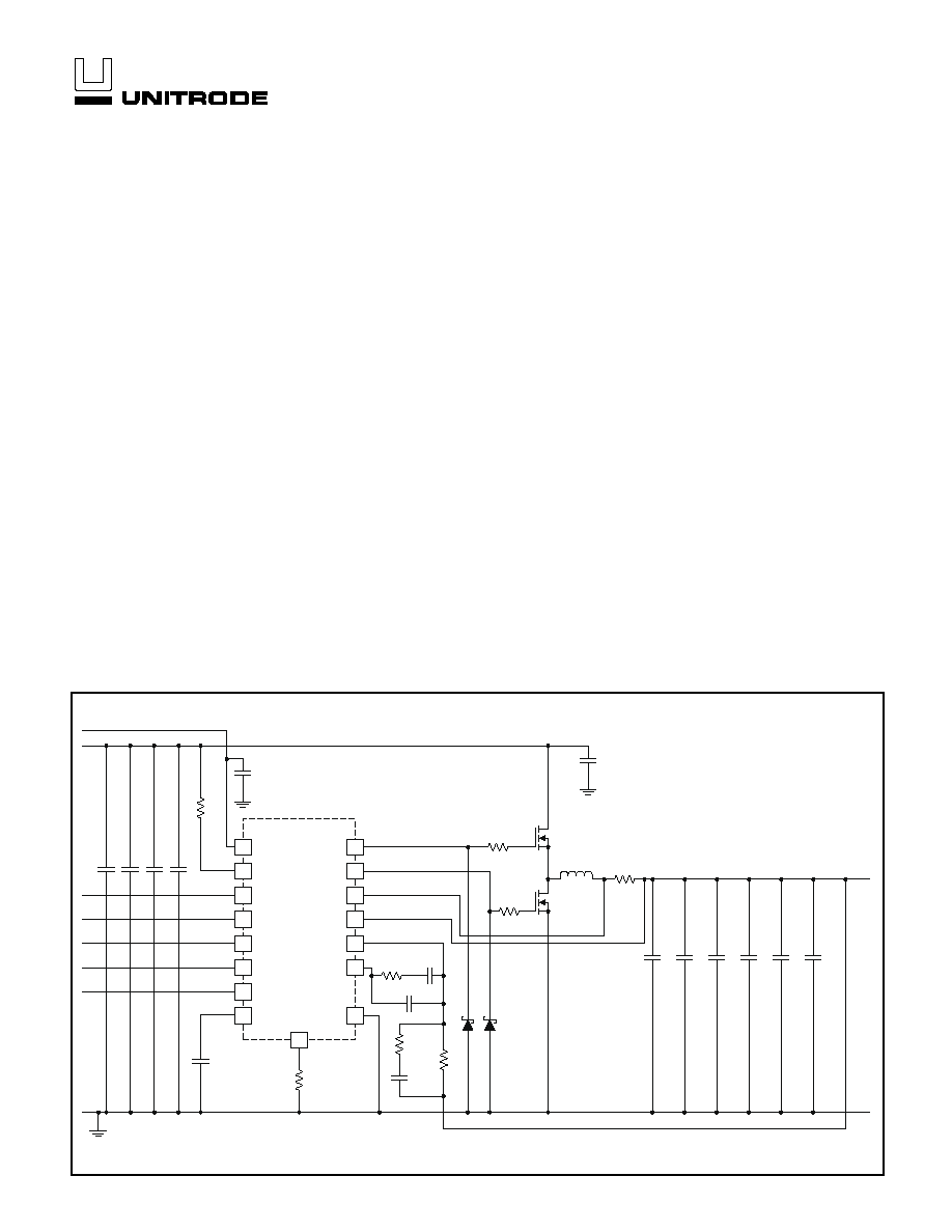
Figure 1 shows a synchronous regulator using the
UCC3588. It accepts +5V and +12V as input, and deliv-
ers a regulated DC output voltage. The value of the out-
put voltage is programmable via a 5-bit DAC code to a
value between 1.3V and 3.5V. The example given here is
for a 12A regulator, running from a 10% tolerance
source, and operating at 300kHz.
The design of the power stage is straightforward buck
regulator design. Assuming an output noise requirement
of 50mV, and an output ripple current of 20% of full load,
the value of the output inductor should be calculated at
the highest input voltage and lowest output voltage that
the regulator is likely to see. This insures that the ripple
current will decrease as the input voltage and output volt-
age differential decreases. The minimum duty cycle,
min
,
should also be calculated under this condition.
1) The current sense resistor is chosen to allow current
limit to occur at 1.4 times the full load current.
(
)
R
V
I
mV
A
m
TRIP
OUT
6
1 4
50
16 8
3
=
∑
=
=
.
.
(3)
2) To properly approximate the full load duty cycle oper-
ating range, assumptions are made regarding the
MOSFETs' Rds
ON
, and the output inductor's DC resis-
tance. Q1 and Q2 are IRF3103s, each with an Rds
ON
of
0.014
. The output inductor is allowed to dissipate one
watt under full load, giving a DC resistance of 6.9m
,
and R6 is 3m
. The resulting duty cycle at the operating
extremes is then:
( )
(
)
( )
(
)
min
.
.
.
=
+
∑
+
+
=
+
∑
=
V
I
R
Rds
R
V
OUT lo
OUT
ON
IN hi
6
1 8
12 0 024
5 5
0 379
.
(4)
( )
(
)
( )
(
)
max
.
.
.
=
+
∑
+
+
=
+
∑
=
V
I
R
Rds
R
V
OUT hi
OUT
ON
IN lo
6
3 5
12 0 024
4 5
0 842
.
(5)
3) The value of the output inductor is chosen at the worst
case ripple current point.
APPLICATION INFORMATION
4
11
15
5
6
7
8
3
16
12
9
10
1
2
14
13
UCC3588
VCC
DRVHI
PWRGOOD
D0
D1
D2
D3
D4
SS/ENBL
GND
COMP
VFB
VSENSE
ISNS
DRVLO
RT
R2
47k
C5
33nF
C16
10
µ
F
R1
10K
C4
C3
C2
C1
+
+
+
+
RTN
D0
D1
D2
D3
D4
R3
200k
C6
220pF
C7 22pF
R7
15k
C13
1nF
R8
20k
R4
3
R5
3
R6
0.003
C15
150
µ
F
C12
C11
C10
C8
+
+
RTN
VOUT
L1
1.6
µ
H
Q2
IRL3103
Q1
IRL3103
D2
D1
12V IN
5V IN
C8-C12 1500
µ
F
+
+
+
C1-C4
1500
µ
F
+
C14
150
µ
F
C9
+
APPLICATION DIAGRAM
UDG-98158

7
UCC3588
( )
( )
(
)
(
)
L
V
V
T
I
IN hi
OUT lo
S
OUT
=
-
∑
=
-
∑
∑
µ
min
.
.
.
.
.
5 5 1 8
0 379 3 333
2 4
=
1 9
.
µ
H
(6)
Four turns of #16 on a micrometals T51-52C core has an
inductance of 1.9
µ
H, has a DC resistance of 6.6m
, and
will dissipate about 1W under full load conditions. With
an output inductor value of 1.9
µ
H, the ripple current will
be 1750mA under the low-input-high-output condition.
4) To meet the output noise voltage requirement, the out-
put capacitor(s) must be chosen so that the ripple volt-
age induced across the ESR of the capacitors by the
output ripple current is less than 50mv.
ESR
mV
I
m
OUT
<
=
50
42
(7)
Additionally, to meet output load transient response re-
quirements, the capacitors' ESL and ESR must be low
enough to avoid excessive voltage transient spikes. (See
Application Note U-157 for a discussion of how to deter-
mine the amount and type of load capacitance.) For this
example, four Sanyo MV-GX 1500
µ
f, 6.3V capacitors will
be used. The ESR of each capacitor is approximately
44m
so the parallel combination of four results in an
equivalent ESR of 11m
.
5) Q1 and Q2 are chosen to be IRF3103 N-Channel
MOSFETs. Each MOSFET has an Rds
ON
of approxi-
mately 0.014
, a gate charge requirement of 50nC, and
a turn OFF time of approximately 54ns.
To calculate the losses in the upper MOSFET, Q1, first
calculate the RMS current it will be conducting.
(
)
I Q
I
I
RMS
OUT
OUT
1
12
2
2
=
+
(8)
Notice that with a higher output voltage, the duty cycle in-
creases, and therefore so does the RMS current. Any
heat sink design should take into account the worst case
power dissipation the device will experience.
With the highest programmable output voltage of 3.5
volts and the lowest possible input voltage of 4.5V, the
RMS current Q1 will conduct is 10.5 amps, and the con-
duction loss is
(
)
P
Q
I
Rds
W
CON
Q RMS
ON
1
1 5
1
2
=
∑
=
.
(9)
Next, the gate drive losses are found.
( )
P
Q
Q
V
F
W
GATE
G
IN hi
S
1
0 0 8
=
∑
∑
=
.
(10)
And the Turn OFF losses are estimated as
(
)
( )
( )
P
Q
V
I
tf
F
W
T OFF
IN hi
D pk
S
1
0 56
1
2
=
∑
∑ ∑
=
.
(11)
The total loss in Q1is the sum of the three components,
or about 2.1 watts.
The gate drive losses in Q2 will be the same as in Q1,
but the turn OFF losses will be associated with the re-
verse recovery of the body diode, instead of the turn OFF
of the channel. This is due to the UCC3588's delay built
into the switching of the upper and lower MOSFET's
drive. For example, when Q1 is turned OFF, the turn ON
of Q2 is delayed for about 100ns, insuring that the circuit
has time to commutate and that current has begun to
flow in the body diode of Q2. When Q2 is turned OFF,
current is diverted from the channel of Q2 into the body
diode of Q2, resulting in virtually no power dissipation.
When Q1 is turned ON 100ns later however, the circuit is
forced to commutate again. This time causing reverse re-
covery loss in the body diode of Q2 as its polarity is re-
versed. The loss in the diode is expressed as:
P
Q
Q
V
F
W
RR
RR
IN hi
S
2
0 26
1
2
= ∑
∑
∑
=
( )
.
(12)
Where Q
RR
, the reverse recovery of the body diode, is
310nC.
100ns before the turn ON of Q2, and 100ns after the turn
OFF of Q2, current flows through Q2's intrinsic body di-
ode. The power dissipation during this interval is:
P
Q
I
V
ns
s
W
COM
DIODE
OUT
DIODE
2
200
3 33
12 1 4 0 0 6 1
=
∑
∑
=
∑
∑
=
.
.
.
µ
(13)
During the ON period of Q2, current flows through the
Rds
ON
of the device. Where the highest RMS current in
Q1 was at the low-input-and-high-output condition, the
highest RMS current in Q2 is found when the input is at
its highest, and the output is at its lowest. The equation
for the RMS current in Q2 is:
(
)
I Q
ns
s
I
I
RMS
OUT
OUT
2
1
200
3 33
12
2
2
=
-
-
∑
+
µ
min
.
=
8 7
.
A
(14)
(
)
P
Q
I Q
Rds
W
CON
RMS
ON
2
2
1 06
2
=
∑
=
.
(15)
The worst case loss in Q2 comes to about 2.4 watts.
6) Repeating the preceding procedure for various input
and output voltage combinations yields a table of operat-
ing conditions.
APPLICATION INFORMATION (cont.)
8
UCC3588
7) Assuming the converter's input current is DC, the re-
maining switching current drawn by Q1 must come from
the input capacitors. The next step then, is to find the
worst case RMS current the capacitors will experience.
(Equation 16). Where I
IN
(avg) is the average input cur-
rent.
Repeating the above calculation over the operating range
of the regulator (see Table 2.) reveals that the worst case
capacitor ripple current is found at low input, and at low
output voltage. A Sanyo MV-GX, 1500
µ
F, 6.3V capacitor
is rated to handle 1.25 amps at 105∞C. Derating the de-
sign to 70∞C allows the use of four capacitors, each one
experiencing one fourth of the total ripple current.
8) The voltage feedback loop is next. The gain and fre-
quency response of the PWM and LC filter is shown in
Equation 17.
To compensate the loop with as high a bandwidth as
practical, additional gain is added to the loop with the
voltage error amplifier.
APPLICATION INFORMATION (cont.)
V
IN
=
4.5
5.0
5.5
V
OUT
=3.5
Pd Q1
Pd Q2
Pd L
Pd Total
Average Input
Duty Cycle
2.2
1.5
0.95
5.1
10.50
0.84
2.1
1.6
0.95
5.2
9.5
0.76
2
1.8
0.95
5.4
8.70
0.69
V
OUT
=1.8
Pd Q1
Pd Q2
Pd L
Pd Total
Average Input
Duty Cycle
1.5
2.3
0.95
5.2
6.00
0.46
1.4
2.4
0.95
5.3
5.40
0.42
1.4
2.5
0.95
5.4
4.96
0.38
Table 1. Regulator Operating Conditions
V
IN
=
4.5
5.0
5.5
V
OUT
= 3.5
Total Input Cap RMS Current
Total Input Cap Power Dissipation
Total Power Dissipation
Power Train Efficiency
4.4
0.21
5.1
0.89
5.2
0.29
5.3
0.88
5.6
0.34
5.4
0.87
V
OUT
=1.8
Total Input Cap RMS Current
Total Input Cap Power Dissipation
Total Power Dissipation
Power Train Efficiency
6
0.39
5.2
0.81
5.9
0.39
5.3
0.8
5.8
0.37
5.4
0.8
Table 2. Regulator Operating Conditions
-60
-50
-40
-30
-20
-10
0
10
20
0.1
1
10
100
1000
FREQUENCY (kHz)
GAIN
(dB)
VIN = 4.5V
VIN = 5.5V
-180
-90
0
90
180
0.1
1
10
100
1000
FREQUENCY (kHz)
PHASE
(∞)
Figure 1. Modulator Frequency Response
(
)
(
)
(
)
I
I
I
I
I
CAP
OUT
IN avg
OUT
IN avg
RMS
=
-
+
+ - ∑
2
2
2
12
1
(16)
( )
(
)
K
f
V
V
f
R
C
f
LC
R
R
PWM
IN
RAMP
ESR
OUT
OUT
=
=
+
∑
∑
-
∑
∑
+
+
1 2
1
4
6
2
2
(
)
+
∑
+
R
C
L
R
ESR
OUT
LOAD
(17)
9
UCC3588
The equation for the gain of the voltage amplifier in this
configuration is:
(
)
(
)
(
)
(
)
(
)
(
)
(
)
(
)
(
)
K
s C Rf
s C
R
R
R s C C Rf
s C
C
s C R
EA
I
I
=
+
∑ +
+
+
+
∑ +
1
1
1
3
2
1 2
1
2
1
3
2
2
(18)
For good transient response, select the R
F
-C1 zero at
5kHz. Add additional phase margin by placing the R
I
-C3
zero also at 5kHz. To roll off the gain at high frequency,
selece the R2-C3 pole to be at 10kHz, and the final C2-
R
F
pole at 40kHz. Results are R
I
=20k, R
F
=200k,
R2=15k, C1=220pF, C2=20pF, C3=1000pF. The Gain-
Phase plots of the voltage error amplifier and the overall
loop are plotted below.
9) The value of RT is given by:
RT
F
pF
k
S
=
∑
-
=
1
67 2
800
48
.
(19)
10) The value of the soft start capacitor is given by:
C
t
V
SS
SS
=
∑
10
3 7
µ
.
(20)
Where t
SS
is the desired soft start time.
To insure that soft start is long enough so that the con-
verter does not enter current limit during startup, the
minimum value of soft start may be determined by:
C
C
I
V
R
I
V
V
SS
OUT
CH
LIM
SENSE
OUT
IN
RAMP
∑
-
∑
(21)
Where C
OUT
is the output capacitance, Ich is the soft
start charging current (10
µ
A typ), V
LIM
is the current limit
trip voltage (54mV typ), I
OUT
is the load current, V
IN
is
the 5V supply, and V
RAMP
is the internal oscillator ramp
voltage (1.85V typ). For this example, C
SS
must be
greater than 35nF, and the resulting soft start time will be
13ms.
11) The output of the regulator is adjustable by program-
ming the following codes into the D0 - D4 pins according
to the table below. To program a logic zero, ground the
pin. To program a logic 1, then leave the pin floating. Do
not tie the pin to an external voltage source.
12) A series resistor should be placed in series with the
gate of each MOSFET to prevent excessive ringing due
to parasitic effects. A value of 3
to 5
is usually suffi-
cient in most cases. Additionally, to prevent pins 13 and
14 from ringing more than 0.5V below ground, a clamp
schottky rectifier placed as close as possible to the IC is
also recommended.
APPLICATION INFORMATION (cont.)
+
≠
C1
C2
C3
R2
R
I
R
F
V
IN
V
REF
V
OUT
Figure 3. Voltage error amplifier configuration.
-40
-20
0
20
40
60
0.1
1
10
100
1000
FREQUENCY (kHz)
GAIN
(dB)
Error Amp
VIN = 4.5V
VIN = 5.5V
Figure 4. Error amplifier and loop frequency
response.
0
20
40
60
80
100
120
140
160
180
0.1
1
10
100
1000
FREQUENCY (kHz)
PHASE
(deg)
Error Amp
VIN = 4.5V
VIN = 5.5V
Figure 5. Error amplifier and loop frequency
response.

10
UCC3588
UNITRODE CORPORATION
7 CONTINENTAL BLVD. ∑ MERRIMACK, NH 03054
TEL. (603) 424-2410 ∑ FAX (603) 424-3460
APPLICATION INFORMATION (cont.)
D4
D3
D2
D1
D0
V
OUT
0
1
1
1
1
1.3
0
1
1
1
0
1.35
0
1
1
0
1
1.4
0
1
1
0
0
1.45
0
1
0
1
1
1.5
0
1
0
1
0
1.55
0
1
0
0
1
1.6
0
1
0
0
0
1.65
0
0
1
1
1
1.7
0
0
1
1
0
1.75
0
0
1
0
1
1.8
0
0
1
0
0
1.85
0
0
0
1
1
1.9
0
0
0
1
0
1.95
0
0
0
0
1
2
0
0
0
0
0
2.05
1
1
1
1
1
No
outputs
1
1
1
1
0
2.1
1
1
1
0
1
2.2
1
1
1
0
0
2.3
1
1
0
1
1
2.4
1
1
0
1
0
2.5
1
1
0
0
1
2.6
1
1
0
0
0
2.7
1
0
1
1
1
2.8
1
0
1
1
0
2.9
1
0
1
0
1
3
1
0
1
0
0
3.1
1
0
0
1
1
3.2
1
0
0
1
0
3.3
1
0
0
0
1
3.4
1
0
0
0
0
3.5
Table 3.
VID Codes and Resulting Regulator Output Voltage

IMPORTANT NOTICE
Texas Instruments and its subsidiaries (TI) reserve the right to make changes to their products or to discontinue
any product or service without notice, and advise customers to obtain the latest version of relevant information
to verify, before placing orders, that information being relied on is current and complete. All products are sold
subject to the terms and conditions of sale supplied at the time of order acknowledgement, including those
pertaining to warranty, patent infringement, and limitation of liability.
TI warrants performance of its semiconductor products to the specifications applicable at the time of sale in
accordance with TI's standard warranty. Testing and other quality control techniques are utilized to the extent
TI deems necessary to support this warranty. Specific testing of all parameters of each device is not necessarily
performed, except those mandated by government requirements.
CERTAIN APPLICATIONS USING SEMICONDUCTOR PRODUCTS MAY INVOLVE POTENTIAL RISKS OF
DEATH, PERSONAL INJURY, OR SEVERE PROPERTY OR ENVIRONMENTAL DAMAGE ("CRITICAL
APPLICATIONS"). TI SEMICONDUCTOR PRODUCTS ARE NOT DESIGNED, AUTHORIZED, OR
WARRANTED TO BE SUITABLE FOR USE IN LIFE-SUPPORT DEVICES OR SYSTEMS OR OTHER
CRITICAL APPLICATIONS. INCLUSION OF TI PRODUCTS IN SUCH APPLICATIONS IS UNDERSTOOD TO
BE FULLY AT THE CUSTOMER'S RISK.
In order to minimize risks associated with the customer's applications, adequate design and operating
safeguards must be provided by the customer to minimize inherent or procedural hazards.
TI assumes no liability for applications assistance or customer product design. TI does not warrant or represent
that any license, either express or implied, is granted under any patent right, copyright, mask work right, or other
intellectual property right of TI covering or relating to any combination, machine, or process in which such
semiconductor products or services might be or are used. TI's publication of information regarding any third
party's products or services does not constitute TI's approval, warranty or endorsement thereof.
Copyright
©
1999, Texas Instruments Incorporated