
UCC3588
5 BIT PROGRAMMABLE OUTPUT BiCMOS
POWER SUPPLY CONTROLLER
SLUS311A ≠ JULY 1999 ≠ REVISED AUGUST 2000
1
POST OFFICE BOX 655303
∑
DALLAS, TEXAS 75265
D
5-Bit Digital-to-Analog Converter (DAC)
supports Intel Pentium II
D
Microprocessor VID Codes
D
Compatible with 5-V or 12-V Systems
D
1% Output Voltage Accuracy Ensured
D
Drives 2 N-Channel MOSFETs
D
Programmable Frequency to 800 kHz
D
Power Good OV / UV / OVP Voltage Monitor
D
Undervoltage Lockout and Softstart
Functions
D
Short Circuit Protection
D
Low Impedance MOSFET Drivers
D
Chip Disable
AVAILABLE OPTIONS
TJ
PACKAGED DEVICES
TJ
D, 16-PIN
J, 16-PIN
N, 16-PIN
PW, 16-PIN
0
∞
C TO 70
∞
C
UCC3588D
UCC3588J
UCC3588N
UCC3588PW
description
The UCC3588 synchronous step-down (Buck) regulator provides accurate high efficiency power conversion.
Using few external components, the UCC1588 converts 5V to an adjustable output ranging from 3.5 VDC to
2.1 VDC in 100-mV steps and 2.05 VDC to 1.3 VDC in 50-mV steps with 1% dc system accuracy. A high level
of integration and novel design allow this 16-pin controller to provide a complete control solution for today's
demanding microcontroller power requirements. Typical applications include on board or VRM based power
conversion for Intel Pentium II microprocessors, as well as other processors from a variety of manufacturers.
High efficiency is obtained through the use of synchronous rectification.
The softstart function provides a controlled ramp up of the system output voltage. Overcurrent circuitry detects
a hard (or soft) short on the system output voltage and invokes a timed softstart/shutdown cycle to reduce the
PWM controller on time to 5%.
The oscillator frequency is externally programmed with RT and operates over a range of 50 kHz to 800 kHz.
The gate drivers are low impedance totem pole output stages capable of driving large external MOSFETs. Cross
conduction is eliminated by fixed delay times between turn off and turn on of the external high side and
synchronous MOSFETs. The chip includes undervoltage lockout circuitry which assures the correct logic states
at the outputs during power up and power down.
This device is available in 16-pin surface mount, plastic and ceramic DIP, and TSSOP packages. The UCC3588
is specified for operation from 0
∞
C to 70
∞
C.
Copyright
2000, Texas Instruments Incorporated
PRODUCTION DATA information is current as of publication date.
Products conform to specifications per the terms of Texas Instruments
standard warranty. Production processing does not necessarily include
testing of all parameters.
Please be aware that an important notice concerning availability, standard warranty, and use in critical applications of
Texas Instruments semiconductor products and disclaimers thereto appears at the end of this data sheet.
1
2
3
4
5
6
7
8
16
15
14
13
12
11
10
9
VSENSE
ISNS
SS/ENBL
D0
D1
D2
D3
D4
RT
VCC
DRVLO
DRVHI
GND
PWRGOOD
VFB
COMP
D, J, N AND PW PACKAGES
(TOP VIEW)
UCC3588
5 BIT PROGRAMMABLE OUTPUT BiCMOS
POWER SUPPLY CONTROLLER
SLUS311A ≠ JULY 1999 ≠ REVISED AUGUST 2000
2
POST OFFICE BOX 655303
∑
DALLAS, TEXAS 75265
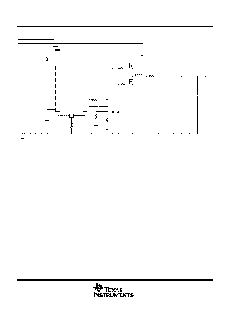
application diagram
4
11
15
5
6
7
8
3
16
12
9
10
1
2
14
13
UCC3588
VCC
DRVHI
PWRGOOD
D0
D1
D2
D3
D4
SS/ENBL
GND
COMP
VFB
VSENSE
ISNS
DRVLO
RT
R2
47 k
C5
33 nF
C16
10
µ
F
R1
10 k
C4
C3
C2
C1
+
+
+
+
RTN
D0
D1
D2
D3
D4
R3
200 k
C6
220 pF
C7 22 pF
R7
15 k
C13
1 nF
R8
20 k
R4
3
R5
3
R6
0.003
C15
150
µ
F
C12
C11
C10
C8
+
+
RTN
VOUT
L1
1.6
µ
H
Q2
IRL3103
Q1
IRL3103
D2
D1
12 V IN
5 V IN
C8≠C12 1500
µ
F
+
+
+
C1≠C4
500
µ
F
+
C14
150
µ
F
C9
+
UDG-98158
absolute maximum ratings over operating free-air temperature (unless otherwise noted)
Supply voltage V
CC
15 V
. . . . . . . . . . . . . . . . . . . . . . . . . . . . . . . . . . . . . . . . . . . . . . . . . . . . . . . . . . . . . . . . . . . . . . . .
Gate drive current, 50% duty cycle
1 A
. . . . . . . . . . . . . . . . . . . . . . . . . . . . . . . . . . . . . . . . . . . . . . . . . . . . . . . . . . . .
Input voltage, V
SENSE
, V
FB
, SS, COMMAND, COMP
5 V
. . . . . . . . . . . . . . . . . . . . . . . . . . . . . . . . . . . . . . . . . . .
Input voltage, D0, D1, D2, D3, D4
6 V
. . . . . . . . . . . . . . . . . . . . . . . . . . . . . . . . . . . . . . . . . . . . . . . . . . . . . . . . . . . . .
Input current, RT, COMP
5 mA
. . . . . . . . . . . . . . . . . . . . . . . . . . . . . . . . . . . . . . . . . . . . . . . . . . . . . . . . . . . . . . . . . . .
Stresses beyond those listed under "absolute maximum ratings" may cause permanent damage to the device. These are stress ratings only, and
functional operation of the device at these or any other conditions beyond those indicated under "recommended operating conditions" is not
implied. Exposure to absolute-maximum-rated conditions for extended periods may affect device reliability.
Currents are positive into, negative out of the specified terminal. Consult Packaging Section of Databook for thermal limitations and
considerations of packages. All voltages are referenced to GND.
thermal data
Plastic DIP package,
thermal resistance junction to leads,
jc 45
∞
C/W
. . . . . . . . . . . . . . . . . . . . . . . . . . . . . . . . . . . . . . . . . . . . . .
thermal resistance junction to ambient,
ja 90
∞
C/W
. . . . . . . . . . . . . . . . . . . . . . . . . . . . . . . . . . . . . . . . . . . .
Ceramic DIP package,
thermal resistance junction to leads,
jc 28
∞
C/W
. . . . . . . . . . . . . . . . . . . . . . . . . . . . . . . . . . . . . . . . . . . . . .
thermal resistance junction to ambient,
ja 120
∞
C/W
. . . . . . . . . . . . . . . . . . . . . . . . . . . . . . . . . . . . . . . . . . .
Standard surface mount package,
thermal resistance junction to leads,
jc 35
∞
C/W
. . . . . . . . . . . . . . . . . . . . . . . . . . . . . . . . . . . . . . . . . . . . . .
thermal resistance junction to ambient,
ja 120
∞
C/W
. . . . . . . . . . . . . . . . . . . . . . . . . . . . . . . . . . . . . . . . . . .
NOTE The above numbers for
ja and
jc are maximums for the limiting thermal resistance of the package in a standard mounting configuration.
The
ja numbers are meant to be guidelines for the thermal performance of the device and PC board system. All of the above numbers
assume no ambient airflow, see the packaging section of Unitrode Product Data Handbook for more details.
UCC3588
5 BIT PROGRAMMABLE OUTPUT BiCMOS
POWER SUPPLY CONTROLLER
SLUS311A ≠ JULY 1999 ≠ REVISED AUGUST 2000
3
POST OFFICE BOX 655303
∑
DALLAS, TEXAS 75265
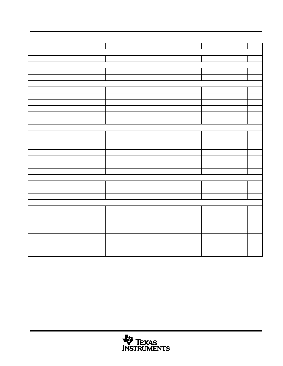
electrical characteristics,
T
A
= 0
∞
C to 70
∞
C. T
A
= T
J
. V
CC
= 12 V, RT = 49 k, (unless otherwise stated)
PARAMETER
TEST CONDITIONS
MIN
TYP
MAX
UNITS
Supply Current Section
Supply current, on
VCC = 12 V,
VRT = 2 V
4.5
5.5
mA
UVLO Section
VCC UVLO turnon threshold
10.05
10.50
10.85
V
UVLO threshold hysteresis
350
450
550
mV
Voltage Error Amplifier Section
Input bias current
VCM = 2.0 V
≠0.025
≠0.050
mA
Open loop gain
See Note 5
77
dB
Output voltage high
ICOMP = ≠500 mA
3.5
3.6
V
Output voltage low
ICOMP = 500 mA
0.2
0.5
V
Output source current
VVFB = 2 V,
VCOMMAND = VCOMP = 2.5 V
≠400
≠500
mA
Output sink current
VVFB = 3 V,
VCOMMAND = VCOMP = 2.5 V
5
10
mA
Oscillator/PWM Section
Initial accuracy
0
∞
C < TA < 70
∞
C
250
270
290
kHz
Ramp amplitude (p≠p)
1.85
V
Ramp valley voltage
0.65
V
PWM max duty cycle
COMP = 3 V
See Note 5
100
%
PWM min duty cycle
COMP = 0. 3 V
See Note 5
0
%
PWM delay to outputs (high to low)
COMP = 1.5 V
See Note 5
150
ns
PWM delay to outputs (low to high)
COMP = 1.5 V
See Note 5
150
ns
Transient Window Comparator Section
Detection range high (duty cycle = 0)
% Over VCOMMAND,
See Note 1
3
%
Detection range low (duty cycle = 1)
% Under VCOMMAND,
See Note 1
≠3
%
Propagation delay (VSENSE to outputs)
150
200
nS
Soft Start/ Shutdown Section
SS charge current (normal start-up)
Measured on SS
≠6
≠12
mA
SS charge current
(short circuit fault condition)
Measured on SS
≠60
≠100
≠120
mA
SS discharge current
(during timeout sequence)
Measured on SS
1
2.5
5
mA
Shutdown threshold
Measured on SS
4.1
4.2
4.3
V
Restart threshold
Measured on SS
0.4
0.5
0.6
V
Soft start complete threshold (normal start≠
up)
Measured on SS
3.5
3.7
3.9
V
NOTES:
1. This percentage is measured with respect to the ideal command voltage programmed by the VID (D0,....,D4) pins and applies to all
DAC codes from 1.3 V to 3.5 V.
2. Reference and error amplifier offset trimmed while the voltage amplifier is set in unity gain mode.
3. Deadtime delay is measured from the 50% point of DRVHI falling to the 50% point of DRVLO rising, and vice-verse.
4. This time is dependent on the value of CSS.
5. Ensured by design. Not 100% production tested.

UCC3588
5 BIT PROGRAMMABLE OUTPUT BiCMOS
POWER SUPPLY CONTROLLER
SLUS311A ≠ JULY 1999 ≠ REVISED AUGUST 2000
4
POST OFFICE BOX 655303
∑
DALLAS, TEXAS 75265
electrical characteristics,
T
A
= 0
∞
C to 70
∞
C. T
A
= T
J
. V
CC
= 12 V, RT = 49 k, (unless otherwise stated)
PARAMETER
TEST CONDITIONS
MIN
TYP
MAX
UNITS
DAC / Reference Section
COMMAND voltage accuracy
10.8 V < VCC < 13.2 V,
measured on COMP,
0
∞
C < TA < 70
∞
C,
See Note 2
≠1.0
1.0
%
D0 to D4 voltage high
5.5
6
6.5
V
D0 to D4 voltage threshold
2.5
3.0
3.5
V
D0 to D4 voltage input bias current
V(D4,...,D0) < 0.5 V
≠80
≠100
mA
Overvoltage Comparator Section
Trip point
% Over VCOMMAND,
See Note 1
8
12
%
Hysteresis
10
20
35
mV
Undervoltage Comparator Section
Trip point
% Under VCOMMAND,
See Note 1
≠8.0
≠12.0
%
Hysteresis
10
20
35
mV
PWRGOOD Signal Section
Output impedance
VCC = 12 V,
IPWRGOOD = 1 mA
470
W
Overvoltage Protection Section
Trip point
% Over VCOMMAND,
See Note 1
15
17.5
20
%
Hysteresis
20
35
mV
VSENSE input bias current
OV, OVP, UV combined
≠8
≠12
≠16
mA
Gate Drivers (DRVHI, DRVLO) Section
Output high voltage
IGATE = 100 mA, VCC = 12 V
10.8
11.5
V
Output low voltage
IGATE =≠100 mA, VCC = 12 V
0.5
0.8
V
Driver non-overlap time
(DRVHI≠ to DRVLO+)
See Note 3
90
120
150
ns
Driver non-overlap time
(DRVLO≠ to DRVHI+)
See Note 3
50
80
120
ns
Driver rise time
3 nF capacitive load
80
100
ns
Driver fall time
3 nF capacitive load
80
100
ns
Current Limit Section
Start of quick charge to shutdown threshold
VISNS = VSENSE + 75 mV, CSS = 10 nF,
See Note 4,
See Note 5
50
ms
Current limit threshold voltage
VTHRESHOLD = VISNS ≠ VVSENSE
40
54
70
mV
ISNS input bias current
≠8
≠12
≠16
mA
NOTES:
6. This percentage is measured with respect to the ideal command voltage programmed by the VID (D0,....,D4) pins and applies to all
DAC codes from 1.3 V to 3.5 V.
7. Reference and error amplifier offset trimmed while the voltage amplifier is set in unity gain mode.
8. Deadtime delay is measured from the 50% point of DRVHI falling to the 50% point of DRVLO rising, and vice-verse.
9. This time is dependent on the value of CSS.
10. Ensured by design. Not 100% production tested.
UCC3588
5 BIT PROGRAMMABLE OUTPUT BiCMOS
POWER SUPPLY CONTROLLER
SLUS311A ≠ JULY 1999 ≠ REVISED AUGUST 2000
5
POST OFFICE BOX 655303
∑
DALLAS, TEXAS 75265
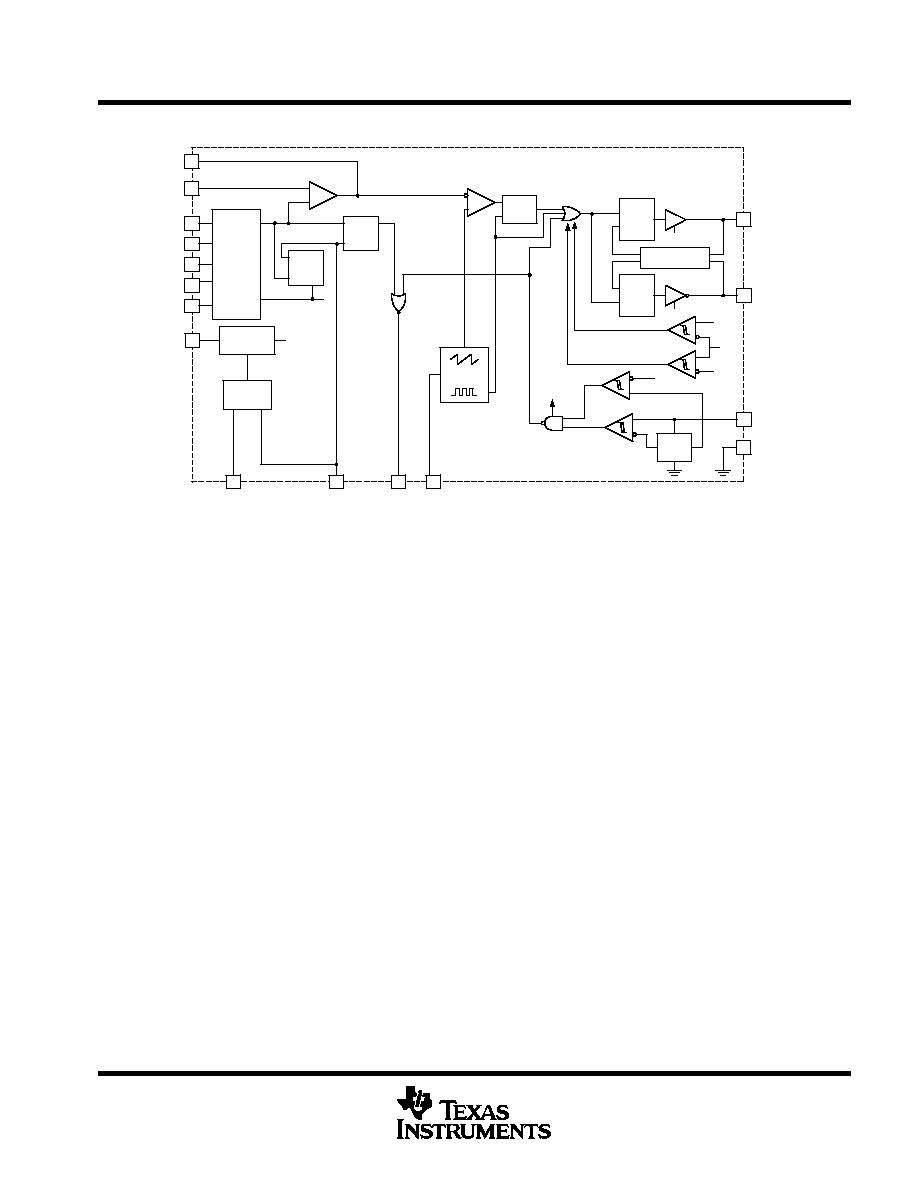
block diagram
10
8
7
6
5
4
3
DAC
OVP
OV/UV
+
≠
9
1
SOFTSTART
CURRENT
LIMIT
BLOCK
OVER≠
CURRENT
2
11
OSC
16
R
S
Q
VREF
15
12
TURN
ON
DELAY
TURN
ON
DELAY
ANTI CROSS≠
CONDUCTION
13
14
VCC
UVLO
10.5 V
VBIAS
VOLTAGE
AMPLIFIER
COMP
VFB
D4
D3
D2
D1
D0
SS/ENBL
ISNS
VSENSE
PWRGOOD RT
GND
VCC
DRVHI
DRVLO
COMMAND
≠3%
COMMAND
+3%
VSENSE
DUTY=1
DUTY=0
SHUTDOWN
PWM
COMP.
COMMAND
SHUTDOWN
TO
VREF
SHUTDOWN
+
+
≠
+
≠
UDG-98152
pin assignments
COMP: (Voltage Amplifier Output) The system voltage compensation network is applied between COMP and
VFB.
D0, D1, D2, D3, D4: These are the digital input control codes for the DAC. The DAC is comprised of two ranges
set by D4, with D0 representing the least significant bit (LSB) and D3, the most significant bit (MSB). A bit is
set low by being connected the pin to GND; a bit is set high by floating the pin. Each control pin is pulled up to
approximately 6 V by an internal pull-up. If one of the low voltage codes is commanded on the DAC inputs, the
outputs will be disabled. The outputs will also be disabled for all 1's, the NO CPU command.
DRVHI: (PWM Output, MOSFET Driver) This output provides a low Impedance totem-pole driver. Use a series
resistor between this pin and the gate of the external MOSFET to prevent excessive overshoot. Minimize circuit
trace length to prevent DRVHI from ringing below GND. DRVHI is disabled during UVLO conditions. DRVHI has
a typical output impedance of 5
for a V
CC
voltage of 12 V.
DRVLO: (synchronous rectifier output, MOSFET driver) This output provides a low Impedance totem-pole
driver to drive the low-side synchronous external MOSFET. Use a series resistor between this pin and the gate
of the external MOSFET to prevent excessive overshoot. Minimize circuit trace length to prevent DRVLO from
ringing below GND. DRVLO is disabled during UVLO conditions. DRVLO has a typical output impedance of 5
for a V
CC
voltage of 12 V.
GND: (Ground) All voltages measured with respect to ground. V
CC
should be bypassed directly to GND with
a 0.1-
µ
F or larger ceramic capacitor. The timing capacitor discharge current also returns to this pin, so the lead
from the oscillator timing to GND should be as short and direct as possible.
ISNS: (Current Limit Sense Input) A resistance connected between this sense connection and V
SENSE
sets up
the current limit threshold (54-mV typical voltage threshold).
PWRGOOD: This pin is an open drain output which is driven low to reset the microprocessor when VSNS rises
above or falls below its nominal value by 8.5%(typ). The on resistance of the open-drain switch is no higher than
470
. This output should be pulled up to a logic level voltage and should be programmed to sink 1 mA or less.
UCC3588
5 BIT PROGRAMMABLE OUTPUT BiCMOS
POWER SUPPLY CONTROLLER
SLUS311A ≠ JULY 1999 ≠ REVISED AUGUST 2000
6
POST OFFICE BOX 655303
∑
DALLAS, TEXAS 75265
pin assignments (continued)
RT: (Oscillator Charging Current) This pin is a low impedance voltage source set at ~1.25 V. A resistor from RT
to GND is used to program the internal PWM oscillator frequency. The equation for R
T
follows:
R
T
+
1
(f
67.2 pF)
*
800
SS/ENBL: (Soft Start/Shut Down) A low leakage capacitor connected between SS and GND will provide a
softstart function for the converter. The voltage on this capacitor will slowly charge on start-up via an internal
current source (10 mA typ.) and ultimately clamp at approximately 3.7 V. The output of the voltage error amplifier
(COMP) tracks this voltage thereby limiting the controller duty ratio. If a short circuit is detected, the clamp is
released and the cap on SS charges with a 100 mA (typ) current source. If the SS voltage exceeds 4.2 V, the
converter shuts down, and the 100-mA current source is switched off. The SS cap will then be discharged with
a 2.5-mA (typ) current sink. When the voltage on SS falls below 0.5 V, a new SS cycle is started. The equation
for softstart time follows:
T
SS
+
3.7
C
SS
10
m
A
Shutdown is accomplished by pulling SS/SD below 0.5 V.
VCC: (Positive Supply Voltage) This pin is normally connected to a 12-V
±
10% system voltage. The UCC1588
will commence normal operation when the voltage on VCC exceeds 10.5 V (typ). Bypass VCC directly to GND
with a 0.1-
µ
F (minimum) ceramic capacitor to supply current spikes required to charge external MOSFET gate
capacitances.
VFB: (Voltage Amplifier Inverting Input) This is normally connected to a compensation network and to the power
converter output through a divider network.
VSENSE: (Direct Output Voltage Connection) This pin is a direct kelvin connection to the output voltage used
for over voltage, under voltage, and current sensing.
APPLICATION INFORMATION
Figure 1 shows a synchronous regulator using the UCC3588. It accepts 5 V and 12 V as input, and delivers a
regulated dc output voltage. The value of the output voltage is programmable via a 5-bit DAC code to a value
between 1.3 V and 3.5 V. The example given here is for a 12-A regulator, running from a 10% tolerance source,
and operating at 300 kHz.
The design of the power stage is straightforward buck regulator design. Assuming an output noise requirement
of 50 mV, and an output ripple current of 20% of full load, the value of the output inductor should be calculated
at the highest input voltage and lowest output voltage that the regulator is likely to see. This insures that the ripple
current will decrease as the input voltage and output voltage differential decreases. The minimum duty cycle,
dmin, should also be calculated under this condition.
1) The current sense resistor is chosen to allow current limit to occur at 1.4 times the full load current.
R6
+
V
TRIP
1.4
I
OUT
+
50 mV
16.8 A
+
3 m
W
(1)
(2)
(3)

UCC3588
5 BIT PROGRAMMABLE OUTPUT BiCMOS
POWER SUPPLY CONTROLLER
SLUS311A ≠ JULY 1999 ≠ REVISED AUGUST 2000
7
POST OFFICE BOX 655303
∑
DALLAS, TEXAS 75265
APPLICATION INFORMATION
2) To properly approximate the full load duty cycle operating range, assumptions are made regarding the
MOSFETs' R
DS(on)
, and the output inductor's dc resistance. Q1 and Q2 are IRF3103s, each with an R
DS(on)
of
0.014
. The output inductor is allowed to dissipate one watt under full load, giving a dc resistance of 6.9 mW,
and R6 is 3 m
. The resulting duty cycle at the operating extremes is then:
d
MIN
+
V
OUT IO
)
I
OUT
R6
)
R
DS on
)
R
V
IN HI
+
1.8
)
(12
0.024)
5.5
+
0.379
d
MIN
+
V
OUT HI
)
I
OUT
R6
)
R
DS on
)
R
V
IN LO
+
3.5
)
(12
0.024)
4.5
+
0.842
3) The value of the output inductor is chosen at the worst case ripple current point.
L
+
V
IN HI
*
V
OUT LO
D
V
OUT
+
(5.5
*
1.8)
0.379
3.333
m
2.4
+
1.9
m
H
Four turns of #16 on a micrometals T51-52C core has an inductance of 1.9
µ
H, has a dc resistance of 6.6 m
,
and will dissipate about 1 W under full load conditions. With an output inductor value of 1.9
µ
H, the ripple current
will be 1750 mA under the low-input-high-output condition.
4) To meet the output noise voltage requirement, the output capacitor(s) must be chosen so that the ripple
voltage induced across the ESR of the capacitors by the output ripple current is less than 50 mV.
ESR
t
50 mV
D
I
OUT
+
42 m
W
Additionally, to meet output load transient response requirements, the capacitors' ESL and ESR must be low
enough to avoid excessive voltage transient spikes. (See Application Note U-157 for a discussion of how to
determine the amount and type of load capacitance.) For this example, four Sanyo MV-GX 1500-
µ
F, 6.3-V
capacitors will be used. The ESR of each capacitor is approximately 44 m
so the parallel combination of four
results in an equivalent ESR of 11 m
.
5) Q1 and Q2 are chosen to be IRF3103 N-Channel MOSFETs. Each MOSFET has an R
DS(on)
of approximately
0.014
, a gate charge requirement of 50 nC, and a turn-off time of approximately 54 ns.
To calculate the losses in the upper MOSFET, Q1, first calculate the RMS current it will be conducting.
I Q1
RMS
+
d
I
OUT2
)
D
I
OUT2
12
Notice that with a higher output voltage, the duty cycle increases, and therefore so does the RMS current. Any
heat sink design should take into account the worst case power dissipation the device will experience.
(4)
(5)
(6)
(7)
(8)

UCC3588
5 BIT PROGRAMMABLE OUTPUT BiCMOS
POWER SUPPLY CONTROLLER
SLUS311A ≠ JULY 1999 ≠ REVISED AUGUST 2000
8
POST OFFICE BOX 655303
∑
DALLAS, TEXAS 75265
APPLICATION INFORMATION
With the highest programmable output voltage of 3.5 V and the lowest possible input voltage of 4.5 V, the RMS
current Q1 will conduct is 10.5 A, and the conduction loss is:
P
CON
Q1
+
I
Q1
RMS
2
R
DS on
+
1.5 W
Next, the gate drive losses are found.
P
CON
Q1
+
Q
G
f
S
+
0.08 W
And the turn-off losses are estimated as
P
T OFF
Q1
+
1
2
V
IN HI
I
D PK
tf
F
S
+
0.56 W
The total loss in Q1is the sum of the three components, or about 2.1 W.
The gate drive losses in Q2 will be the same as in Q1, but the turn-off losses will be associated with the reverse
recovery of the body diode, instead of the turn-off of the channel. This is due to the UCC3588's delay built into
the switching of the upper and lower MOSFET's drive. For example, when Q1 is turned-off, the turn-on of Q2
is delayed for about 100 ns, insuring that the circuit has time to commutate and that current has begun to flow
in the body diode of Q2. When Q2 is turned-off, current is diverted from the channel of Q2 into the body diode
of Q2, resulting in virtually no power dissipation. When Q1 is turned ON 100ns later however, the circuit is forced
to commutate again. This time causing reverse recovery loss in the body diode of Q2 as its polarity is reversed.
The loss in the diode is expressed as:
P
RR
Q2
+
1
2
Q
RR
V
IN HI
F
S
+
0.26 W
Where Q
RR
, the reverse recovery of the body diode, is 310 nC.
100 ns before the turn-on of Q2, and 100 ns after the turn-off of Q2, current flows through Q2's intrinsic body
diode. The power dissipation during this interval is:
P
COM
Q2
DIODE
+
I
OUT
V
DIODE
200 ns
3.33
m
s
+
12
1.4
0.06
+
1 W
During the ON period of Q2, current flows through the R
DS(on)
of the device. Where the highest RMS current
in Q1 was at the low-input and high-output condition, the highest RMS current in Q2 is found when the input
is at its highest, and the output is at its lowest. The equation for the RMS current in Q2 is:
I Q2
RMS
1
* d
MIN
*
200 ns
3.33
m
s
I
OUT
2
) D
I
OUT
2
12
+
+
8.7 A
P
CON
Q2
+
1 Q2
RMS
2
R
DS on
+
1.06 W
The worst case loss in Q2 comes to about 2.4 W.
(9)
(10)
(11)
(12)
(13)
(14)
(15)

UCC3588
5 BIT PROGRAMMABLE OUTPUT BiCMOS
POWER SUPPLY CONTROLLER
SLUS311A ≠ JULY 1999 ≠ REVISED AUGUST 2000
9
POST OFFICE BOX 655303
∑
DALLAS, TEXAS 75265
APPLICATION INFORMATION
6) Repeating the preceding procedure for various input and output voltage combinations yields a table of
operating conditions.
Table 1. Regulator Operating Conditions
VIN=
4.5
5.0
5.5
VOUT = 3.5
Pd Q1
Pd Q2
Pd L
Pd total
Average input
Duty cycle
2.20
1.50
0.95
5.10
10.5
0.84
2.10
1.60
0.95
5.20
9.50
0.76
2.00
1.80
0.95
5.40
8.70
0.69
VOUT = 1.8
Pd Q1
Pd Q2
Pd L
Pd total
Average input
Duty cycle
1.5
2.3
0.95
5.2
6.00
0.46
1.40
2.40
0.95
5.30
5.40
0.42
1.40
2.50
0.95
5.40
4.96
0.38
7) Assuming the converter's input current is dc, the remaining switching current drawn by Q1 must come from
the input capacitors. The next step then, is to find the worst case RMS current the capacitors will experience.
(Equation 16). Where I
IN(avg)
is the average input current.
I
CAP
RMS
+
d
I
OUT
*
I
IN avg
2
)
D
I
OUT
2
12
)
(1
* d
)
I
IN avg
2
Repeating the above calculation over the operating range of the regulator (see Table 2.) reveals that the worst
case capacitor ripple current is found at low input, and at low output voltage. A Sanyo MV-GX, 1500-
µ
F, 6.3-V
capacitor is rated to handle 1.25 A at 105
∞
C. Derating the design to 70
∞
C allows the use of four capacitors, each
one experiencing one fourth of the total ripple current.
8) The voltage feedback loop is next. The gain and frequency response of the PWM and LC filter is shown in
Equation 17.
K
PWM
(f)
+
V
IN
V
RAMP
+
1
)
2
p
f
R
ESR
C
OUT
1
*
4
p
2
f2
LC
OUT
)
R6
)
R
)
R
ESR
C
OUT
)
L
R
LOAD
(16)
(17)

UCC3588
5 BIT PROGRAMMABLE OUTPUT BiCMOS
POWER SUPPLY CONTROLLER
SLUS311A ≠ JULY 1999 ≠ REVISED AUGUST 2000
10
POST OFFICE BOX 655303
∑
DALLAS, TEXAS 75265
APPLICATION INFORMATION
Table 2. Regulator Operating Conditions
VIN=
4.5
5.0
5.5
VOUT=3.5
Total input cap RMS current
Total input cap power dissipation
Total power dissipation
Power train efficiency
4.40
0.21
5.10
0.89
5.20
0.29
5.30
0.88
5.60
0.34
5.40
0.87
VOUT=1.8
Total input cap RMS current
Total input cap power dissipation
Total power dissipation
Power train efficiency
6.00
0.39
5.20
0.81
5.90
0.39
5.30
0.80
5.80
0.37
5.40
0.80
Figure 1
100.0
10.0
1.0
≠50
≠40
≠20
≠10
10
20
≠60
V
IN
= 5.5 V
V
IN
= 4.5 V
1000.0
0.1
≠30
0
GAIN
vs
FREQUENCY
Gain - dB
Frequency - kHz
Figure 2
100.0
10.0
1.0
≠50
≠40
≠20
≠10
10
20
≠60
1000.0
0.1
≠30
0
Frequency - kHz
PHASE
vs
FREQUENCY
Phase -
C
To compensate the loop with as high a bandwidth as practical, additional gain is added to the loop with the
voltage error amplifier.
UCC3588
5 BIT PROGRAMMABLE OUTPUT BiCMOS
POWER SUPPLY CONTROLLER
SLUS311A ≠ JULY 1999 ≠ REVISED AUGUST 2000
11
POST OFFICE BOX 655303
∑
DALLAS, TEXAS 75265
APPLICATION INFORMATION
+
C1
C2
C3
R2
R
I
R
F
V
IN
V
REF
V
OUT
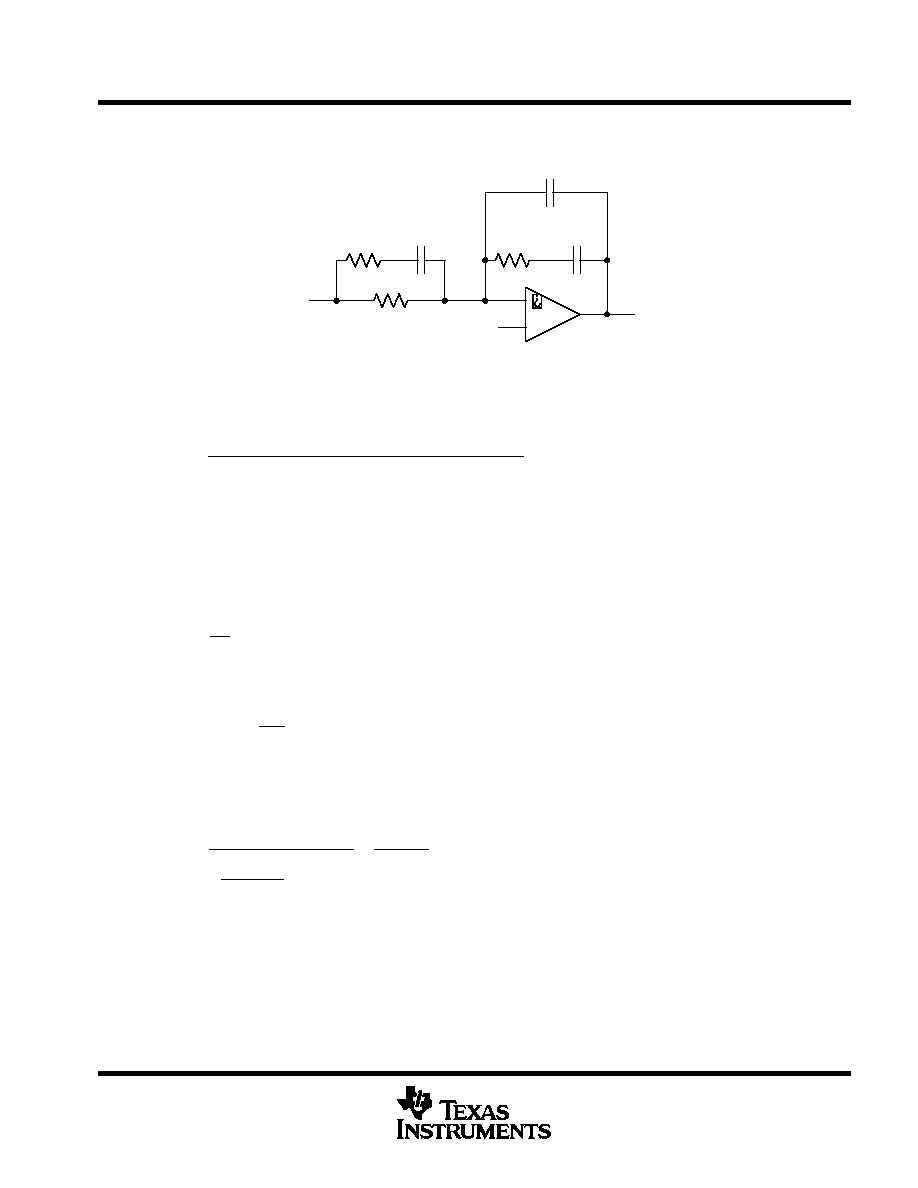
Figure 3. Voltage Error Amplifier Configuration
The equation for the gain of the voltage amplifier in this configuration is:
K
EA
+
(1
)
s(C1Rf))
1
)
s C3 R
I
)
R2
R
I
s2C1C2Rf
)
s(C1
)
C2)
(1
)
s(C3R2))
For good transient response, select the RF-C1 zero at 5 kHz. Add additional phase margin by placing the RI-C3
zero also at 5 kHz. To roll off the gain at high frequency, selece the R2-C3 pole to be at 10 kHz, and the final
C2-RF pole at 40 kHz. Results are RI = 20 k, RF = 200 k, R2 = 15 k, C1 = 220 pF, C2 = 20 pF, C3 = 1000 pF.
The Gain - phase plots of the voltage error amplifier and the overall loop are plotted below.
9) The value of RT is given by:
RT
+
1
F
S
67.2 pF
*
800
+
48 k
W
10) The value of the soft start capacitor is given by:
C
SS
+
10
m
t
SS
3.7
V
Where t
SS
is the desired soft start time.
To insure that soft start is long enough so that the converter does not enter current limit during startup, the
minimum value of soft start may be determined by:
C
SS
w
C
OUT
I
CH
V
LIM
R
SENSE
*
I
OUT
V
IN
V
RAMP
Where C
OUT
is the output capacitance, Ich is the soft start charging current (10 mA typ), V
LIM
is the current limit
trip voltage (54 mV typ), I
OUT
is the load current, V
IN
is the 5-V supply, and V
RAMP
is the internal oscillator ramp
voltage (1.85 V typ). For this example, C
SS
must be greater than 35 nF, and the resulting soft start time will be
13 ms.
(18)
(19)
(20)
(21)

UCC3588
5 BIT PROGRAMMABLE OUTPUT BiCMOS
POWER SUPPLY CONTROLLER
SLUS311A ≠ JULY 1999 ≠ REVISED AUGUST 2000
12
POST OFFICE BOX 655303
∑
DALLAS, TEXAS 75265
APPLICATION INFORMATION
11) The output of the regulator is adjustable by programming the following codes into the D0 - D4 pins according
to the table below. To program a logic zero, ground the pin. To program a logic 1, then leave the pin floating.
Do not tie the pin to an external voltage source.
12) A series resistor should be placed in series with the gate of each MOSFET to prevent excessive ringing due
to parasitic effects. A value of 3
to 5
is usually sufficient in most cases. Additionally, to prevent pins 13 and
14 from ringing more than 0.5-V below ground, a clamp schottky rectifier placed as close as possible to the IC
is also recommended.
Figure 4
VIN = 5.5 V
Error
Amp
VIN = 4.5 V
GAIN
vs
FREQUENCY
Gain - dB
Frequency - kHz
1000
100
10
1
0.1
≠40
≠20
0
20
40
60
Figure 5
0
20
40
60
80
100
120
140
160
180
0.1
1
10
100
1000
Frequency - kHz
PHASE
vs
FREQUENCY
Phase -
C
UCC3588
5 BIT PROGRAMMABLE OUTPUT BiCMOS
POWER SUPPLY CONTROLLER
SLUS311A ≠ JULY 1999 ≠ REVISED AUGUST 2000
13
POST OFFICE BOX 655303
∑
DALLAS, TEXAS 75265
APPLICATION INFORMATION
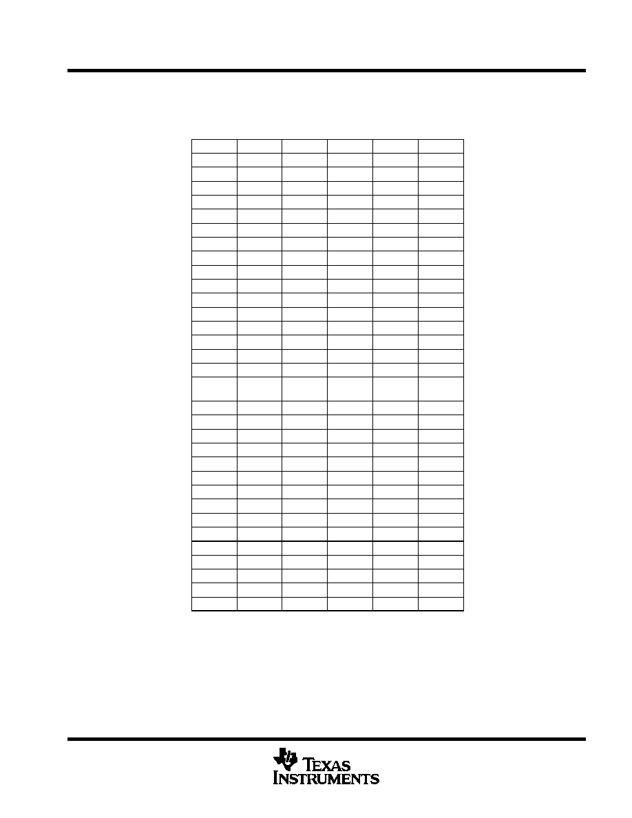
Table 3. VID Codes and Resulting Regulator Output Voltage
D4
D3
D2
D1
D0
VOUT
0
1
1
1
1
1.30
0
1
1
1
0
1.35
0
1
1
0
1
1.40
0
1
1
0
0
1.45
0
1
0
1
1
1.50
0
1
0
1
0
1.55
0
1
0
0
1
1.60
0
1
0
0
0
1.65
0
0
1
1
1
1.70
0
0
1
1
0
1.75
0
0
1
0
1
1.80
0
0
1
0
0
1.85
0
0
0
1
1
1.90
0
0
0
1
0
1.95
0
0
0
0
1
2.00
0
0
0
0
0
2.05
1
1
1
1
1
No out-
puts
1
1
1
1
0
2.10
1
1
1
0
1
2.20
1
1
1
0
0
2.30
1
1
0
1
1
2.40
1
1
0
1
0
2.50
1
1
0
0
1
2.60
1
1
0
0
0
2.70
1
0
1
1
1
2.80
1
0
1
1
0
2.90
1
0
1
0
1
3.00
1
0
1
0
0
3.10
1
0
0
1
1
3.20
1
0
0
1
0
3.30
1
0
0
0
1
3.40
1
0
0
0
0
3.50

UCC3588
5 BIT PROGRAMMABLE OUTPUT BiCMOS
POWER SUPPLY CONTROLLER
SLUS311A ≠ JULY 1999 ≠ REVISED AUGUST 2000
14
POST OFFICE BOX 655303
∑
DALLAS, TEXAS 75265

IMPORTANT NOTICE
Texas Instruments Incorporated and its subsidiaries (TI) reserve the right to make corrections, modifications,
enhancements, improvements, and other changes to its products and services at any time and to discontinue
any product or service without notice. Customers should obtain the latest relevant information before placing
orders and should verify that such information is current and complete. All products are sold subject to TI's terms
and conditions of sale supplied at the time of order acknowledgment.
TI warrants performance of its hardware products to the specifications applicable at the time of sale in
accordance with TI's standard warranty. Testing and other quality control techniques are used to the extent TI
deems necessary to support this warranty. Except where mandated by government requirements, testing of all
parameters of each product is not necessarily performed.
TI assumes no liability for applications assistance or customer product design. Customers are responsible for
their products and applications using TI components. To minimize the risks associated with customer products
and applications, customers should provide adequate design and operating safeguards.
TI does not warrant or represent that any license, either express or implied, is granted under any TI patent right,
copyright, mask work right, or other TI intellectual property right relating to any combination, machine, or process
in which TI products or services are used. Information published by TI regarding third≠party products or services
does not constitute a license from TI to use such products or services or a warranty or endorsement thereof.
Use of such information may require a license from a third party under the patents or other intellectual property
of the third party, or a license from TI under the patents or other intellectual property of TI.
Reproduction of information in TI data books or data sheets is permissible only if reproduction is without
alteration and is accompanied by all associated warranties, conditions, limitations, and notices. Reproduction
of this information with alteration is an unfair and deceptive business practice. TI is not responsible or liable for
such altered documentation.
Resale of TI products or services with statements different from or beyond the parameters stated by TI for that
product or service voids all express and any implied warranties for the associated TI product or service and
is an unfair and deceptive business practice. TI is not responsible or liable for any such statements.
Mailing Address:
Texas Instruments
Post Office Box 655303
Dallas, Texas 75265
Copyright
2001, Texas Instruments Incorporated