
UCC2626, UCC3626
SLUS318B ≠ APRIL 1999 ≠ REVISED JANUARY 2002
BRUSHLESS DC
MOTOR CONTROLLER
1
www.ti.com
FEATURES
D
Two-Quadrant and Four-Quadrant Operation
D
Integrated Absolute Value Current Amplifier
D
Pulse-by-Pulse and Average Current Sensing
D
Accurate, Variable Duty-Cycle Tachometer
Output
D
Trimmed Precision Reference
D
Precision Oscillator
D
Direction Output
DESCRIPTION
The UCC3626 motor controller device combines
many of the functions required to design a
high-performance, two- or four-quadrant, three-
phase, brushless dc motor controller into one
package. Rotor position inputs are decoded to
provide six outputs that control an external power
stage. A precision triangle oscillator and latched
comparator provide PWM motor control in either
voltage- or current-mode configurations. The
oscillator is easily synchronized to an external
master clock source via the SYNCH input.
Additionally, a QUAD select input configures the
chip to modulate either the low-side switches only,
or both upper and lower switches, allowing the
user to minimize switching losses in less
demanding two-quadrant applications.
The device includes a differential current-sense
amplifier and absolute-value circuit which provide
an accurate reconstruction of motor current,
useful for pulse-by-pulse overcurrent protection,
as well as closing a current control loop. A
precision tachometer is also provided for
implementing closed-loop speed control. The
TACH_OUT signal is a variable duty-cycle,
frequency output, which can be used directly for
digital control or filtered to provide an analog
feedback signal. Other features include COAST,
BRAKE, and DIR_IN commands, along with a
direction output, DIR_OUT.
PRODUCTION DATA information is current as of publication date.
Products conform to specifications per the terms of Texas Instruments
standard warranty. Production processing does not necessarily include
testing of all parameters.
Copyright
2002, Texas Instruments Incorporated
UCC2626, UCC3626
SLUS318B ≠ APRIL 1999 ≠ REVISED JANUARY 2002
2
www.ti.com
AVAILABLE OPTIONS
PACKAGED DEVICES
TA
PDIP
(N)
SOIC
{
(DW)
TSSOP
{
(PW)
≠40
_
C to 85
_
C
UCC2626N
UCC2626DW
UCC2626PW
0
_
C to 70
_
C
UCC3626N
UCC3626DW
UCC3626PW
{
The DW and PW packages are available taped and reeled. Add TR suffix to device
type (e.g. UCC2626DWTR) to order quantities of 2,000 devices per reel.
1
2
3
4
5
6
7
8
9
10
11
12
13
14
28
27
26
25
24
23
22
21
20
19
18
17
16
15
GND
VREF
TACH_OUT
R_TACH
C_TACH
CT
SYNCH
DIR_OUT
SNS_NI
SNS_I
IOUT
OC_REF
PWM_I
PWM_NI
VDD
AHI
ALOW
BHI
BLOW
CHI
CLOW
DIR_IN
QUAD
BRAKE
COAST
HALLC
HALLB
HALLA
N PACKAGE
(TOP VIEW)
1
2
3
4
5
6
7
8
9
10
11
12
13
14
28
27
26
25
24
23
22
21
20
19
18
17
16
15
GND
VREF
TACH_OUT
R_TACH
C_TACH
CT
SYNCH
DIR_OUT
SNS_NI
SNS_I
IOUT
OC_REF
PWM_I
PWM_NI
VDD
AHI
ALOW
BHI
BLOW
CHI
CLOW
DIR_IN
QUAD
BRAKE
COAST
HALLC
HALLB
HALLA
DW and PW PACKAGES
(TOP VIEW)
absolute maximum ratings over operating free-air temperature (unless otherwise noted)
Supply voltage V
DD
15 V
. . . . . . . . . . . . . . . . . . . . . . . . . . . . . . . . . . . . . . . . . . . . . . . . . . . . . . . . . . . . . . . . . . . . . . . .
Input voltage,
BRAKE, COAST, DIR_IN, HALLA, HALLB, HALLC,
OC_REF, QUAD, SYNCH, PWM_I, PWM_NI
≠0.3 V to V
DD
. . . . . . . . . . . . . . . . . . . . . . . . . . .
SNS_I, SNS_NI
≠0.5 V to V
DD
. . . . . . . . . . . . . . . . . . . . . . . . . . . . . . . . . . . . . . . . . . . . . . . . . . . . .
Output current AHI, ALOW, BHI, BLOW, CHI, CLOW
±
200 mA
. . . . . . . . . . . . . . . . . . . . . . . . . . . . . . . . . . . . . .
DIR_OUT, IOUT, TACH_OUT,
1 mA
. . . . . . . . . . . . . . . . . . . . . . . . . . . . . . . . . . . . . . . . . . . . . . . .
VREF
≠20 mA
. . . . . . . . . . . . . . . . . . . . . . . . . . . . . . . . . . . . . . . . . . . . . . . . . . . . . . . . . . . . . . . . . . .
Junction temperature range, T
J
≠55
∞
C to 150
∞
C
. . . . . . . . . . . . . . . . . . . . . . . . . . . . . . . . . . . . . . . . . . . . . . . . . . . .
Storage temperature range, T
stg
≠65
∞
C to 150
∞
C
. . . . . . . . . . . . . . . . . . . . . . . . . . . . . . . . . . . . . . . . . . . . . . . . . . . .
Lead temperature soldering 1,6 mm (1/16 inch) from case for 10 seconds
300
∞
C
. . . . . . . . . . . . . . . . . . . . . . .
Stresses beyond those listed under "absolute maximum ratings" may cause permanent damage to the device. These are stress ratings only, and
functional operation of the device at these or any other conditions beyond those indicated under "recommended operating conditions" is not
implied. Exposure to absolute-maximum-rated conditions for extended periods may affect device reliability.
All voltages are with respect to GND. Currents are positive into negative out of the specified terminal.
UCC2626, UCC3626
SLUS318B ≠ APRIL 1999 ≠ REVISED JANUARY 2002
3
www.ti.com
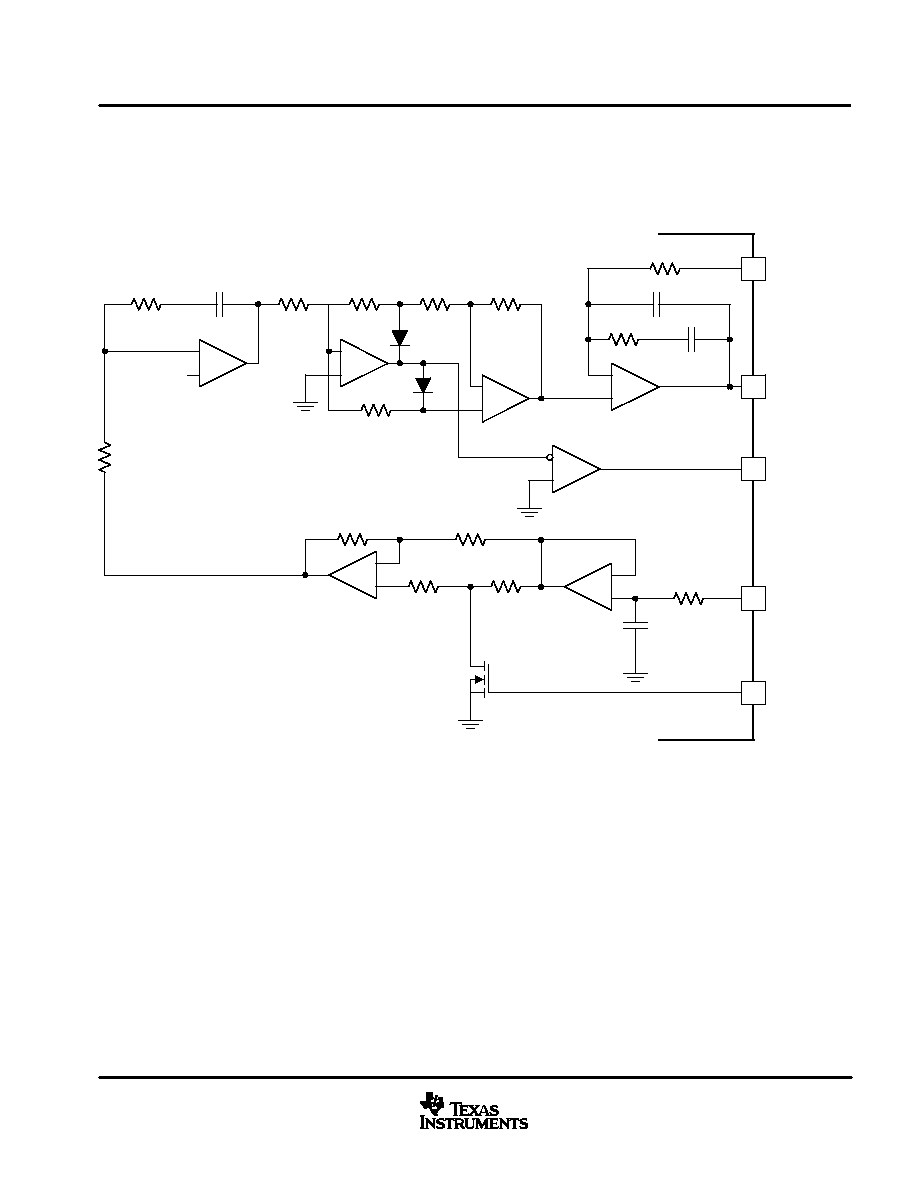
block diagram
UDG≠97173
17
HALLC
8
DIR_OUT
14
PWM_NI
13
PWM_I
16
HALLB
SYNCH
11
OC_REF
9
SNS_I
3
4
1
5
22
CLOW
C_TACH
R_TACH
TACH_OUT
GND
2
VREF
27
AHI
25
BHI
23
CHI
26
ALOW
10
SNS_NI
IOUT
7
6
12
CT
18
COAST
21
DIR_IN
15
HALLA
19
BRAKE
20
QUAD
SENSE AMPLIFIER
OVERCURRENT
COMPARATOR
OSCILLATOR
DIRECTION
DETECTOR
EDGE
DETECTOR
28
VDD
ONE
SHOT
5 VOLT
REFERENCE
S
R
PWM LOGIC
24
BLOW
1.75V
DIRECTION
SELECT
HALL
DECODER
PWM
COMPARATOR
X5
S
R
RxC
Q
Q
Q
Q
UCC2626, UCC3626
SLUS318B ≠ APRIL 1999 ≠ REVISED JANUARY 2002
4
www.ti.com
electrical characteristics over recommended operating conditions, VCC = 12 V; CT = 1 nF,
R_TACH = 250 k
, C_TACH = 100 pF, T
A
= T
J
, T
A
= ≠40
∞
C to 85
∞
C for the UCC2626, and 0
∞
C to 70
∞
C
for the UCC3626 (unless otherwise noted)
overall
PARAMETER
TEST CONDITIONS
MIN
TYP
MAX
UNIT
Supply current
Outputs not switching
1
3
5
mA
undervoltage lockout
PARAMETER
TEST CONDITIONS
MIN
TYP
MAX
UNIT
Start threshold
9.0
10.5
11.0
V
UVLO hysteresis
0.35
0.40
0.50
V
5-V reference
PARAMETER
TEST CONDITIONS
MIN
TYP
MAX
UNIT
Output voltage
IVREF = ≠2 mA
4.9
5
5.1
V
Line regulation voltage
11 V < VCC < 14.5 V
10
mV
Load regulation voltage
≠1 mA > IVREF > ≠5 mA
10
mV
Short circuit current
40
120
240
mA
coast input comparator
PARAMETER
TEST CONDITIONS
MIN
TYP
MAX
UNIT
Threshold voltage
1.60
1.75
2.00
V
Hysteresis
0.04
0.10
0.16
V
current sense amplifier
PARAMETER
TEST CONDITIONS
MIN
TYP
MAX
UNIT
Input offset voltage
VCM = 0 V
8
mV
Input bias current
VCM = 0 V
5
10
15
µ
A
Gain
VCM = 0 V
4.85
5.00
5.15
V/V
PSRR
11 V < VCC < 14.5 V
60
dB
High-level output voltage
IIOUT= ≠100
µ
A
6.3
V
Low-level output voltage
IIOUT = 100
µ
A
70
mV
Output source current
UCC3626
VIOUT = 2 V
500
µ
A
Output source current
UCC2626
VIOUT = 2 V
300
µ
A
pwm comparator
PARAMETER
TEST CONDITIONS
MIN
TYP
MAX
UNIT
Input common mode range
2.0
8.0
V
Propagation delay time
75
150
ns
overcurrent comparator
PARAMETER
TEST CONDITIONS
MIN
TYP
MAX
UNIT
Input common mode range
0.0
5.0
V
Propagation delay time
50
175
250
ns
logic inputs
PARAMETER
TEST CONDITIONS
MIN
TYP
MAX
UNIT
High-level logic input voltage
QUAD, BRAKE, DIR, SYNCH
3.6
V
Low-level logic input voltage
QUAD, BRAKE, DIR, SYNCH
1.4
V

UCC2626, UCC3626
SLUS318B ≠ APRIL 1999 ≠ REVISED JANUARY 2002
5
www.ti.com
electrical characteristics over recommended operating conditions, VCC = 12 V; CT = 1 nF,
R_TACH = 250 k
, C_TACH = 100 pF, T
A
= T
J
, T
A
= ≠40
∞
C to 85
∞
C for the UCC2626, and 0
∞
C to 70
∞
C
for the UCC3626 (unless otherwise noted)
hall buffer inputs
PARAMETER
TEST CONDITIONS
MIN
TYP
MAX
UNIT
High-level input voltage
HALLA, HALLB, HALLC
1.7
1.9
2.1
V
Hysteresis
HALLA, HALLB, HALLC
0.6
1.0
V
Input current
0V < VIN < 5 V
≠25
µ
A
oscillator
PARAMETER
TEST CONDITIONS
MIN
TYP
MAX
UNIT
Frequency
RTACH = 250 k
, CT = 1nF
9.0
10.0
11.0
kHz
Frequency change with voltage
12 V < VCC < 14.5 V
3%
CT peak voltage
7.25
7.5
7.75
V
CT peak-to-valley voltage
4.75
5.0
5.25
V
SYNCH pin minimum pulse width
500
ns
tachometer
PARAMETER
TEST CONDITIONS
MIN
TYP
MAX
UNIT
High-level output voltage/VREF
IOUT = ≠10
µ
A
99%
100%
Low-level output voltage
IOUT = 10
µ
A
0
20
mV
High-level on-resistance
IOUT = ≠100
µ
A
1
1.5
k
Low-level on-resistance
IOUT = 100
µ
A
1
1.5
k
High-level ramp threshold voltage
2.5
V
Ramp voltage
2.375
2.500
2.625
V
CTACH charge current
RTACH = 49.9 k
48
51
53
µ
A
On time accuracy
UCC3626
See Note 1
≠3%
3%
On-time accuracy
UCC2626
See Note 1
≠4%
3%
direction output
PARAMETER
TEST CONDITIONS
MIN
TYP
MAX
UNIT
High-level output voltage
IOUT = ≠100
µ
A
4.5
5.2
V
Low-level output voltage
IOUT = 100
µ
A
0
0.5
V
output
PARAMETER
TEST CONDITIONS
MIN
TYP
MAX
UNIT
Maximum duty cycle
100%
Lo
le el o tp t oltage
IOUT = 2 mA
0.0
0.1
0.5
V
Low-level output voltage
IOUT = 100
µ
A
0.0
0.1
V
High level output voltage
IOUT = ≠2 mA
4.0
4.8
5.2
V
High-level output voltage
IOUT = ≠100
µ
A
4.7
5.2
V
Rise and fall time
CI = 10 pF
100
ns
NOTE 1: tON is calculated using the formula t
ON
+
C
TACH
V
HI
*
V
LO
I
CHARGE

UCC2626, UCC3626
SLUS318B ≠ APRIL 1999 ≠ REVISED JANUARY 2002
6
www.ti.com
pin descriptions
AHI, BHI, CHI: Digital outputs used to control the high-side switches in a three-phase inverter. For specific
decoding information reference Table I.
ALOW, BLOW, CLOW: Digital outputs used to control the low-side switches in a three-phase inverter. For
specific decoding information reference Table I.
BRAKE: BRAKE is a digital input which causes the device to enter brake mode. In brake mode all three high-
side outputs (AHI, BHI & CHI) are turned off, while all three lowside outputs (ALOW, BLOW, CLOW) are turned
on. During brake mode the tachometer output remains operational. The only conditions that can inhibit the
low-side commands during brake are UVLO, exceeding peak current, the output of the PWM comparator, or
the COAST command.
COAST: The COAST input consists of a hysteretic comparator which disables the outputs. The input is useful
in implementing an overvoltage bus clamp in four-quadrant applications. The outputs are disabled when the
input is above 1.75 V.
CT: This pin is used in conjunction with the R_TACH pin to set the frequency of the oscillator. A timing capacitor
is normally connected between this point and ground and is alternately charged and discharged between 2.5 V
and 7.5 V.
C_TACH: A timing capacitor is connected between this pin and ground to set the width of the TACH_OUT pulse.
The capacitor is charged with a current set by the resistor on pin R_TACH .
DIR_IN: DIR_IN is a digital input which determines the order in which the HALLA, HALLB, and HALLC inputs
are decoded. For specific decode information reference Table I.
DIR_OUT: DIR_OUT represents the actual direction of the rotor as decoded from the HALLA, HALLB, and
HALLC inputs. For any valid combination of HALLA, HALLB, and HALLC inputs there are two valid transitions;
one of which translates to a clockwise rotation and another which translates to a counterclockwise rotation. The
polarity of DIR_OUT is the same as DIR_IN while motoring, (i.e. sequencing from top to bottom in Table 1.)
GND: GND is the reference ground for all functions of the part. Bypass and timing capacitors should be
terminated as close as possible to this point.
HALLA, HALLB, HALLC: These three inputs are designed to accept rotor position information positioned 120
∞
apart. For specific decode information reference Table I. These inputs should be externally pulled up to VREF
or another appropriate external supply.
IOUT: IOUT represents the output of the current sense and absolute value amplifiers. The output signal
appearing is a representation of the following expression:
I
OUT
+
ABS I
SNS_I
*
I
SNS_NI
5
This output can be used to close a current control loop as well as provide additional filtering of the current sense
signal.
OC_REF: OC_REF is an analog input which sets the trip voltage of the overcurrent comparator. The sense input
of the comparator is internally connected to the output of the current sense amplifier and absolute value circuit.
PWM_NI: PWM_NI is the noninverting input to the PWM comparator.
PWM_I: PWM_I is the inverting input to the PWM comparator.
QUAD: The QUAD input selects between two-quadrant operation (QUAD = 0) and four-quadrant operation
(QUAD = 1) . When in two-quadrant mode, only the low-side devices are effected by the output of the PWM
comparator. In four-quadrant mode both high- and low-side devices are controlled by the PWM comparator.
UCC2626, UCC3626
SLUS318B ≠ APRIL 1999 ≠ REVISED JANUARY 2002
7
www.ti.com
pin descriptions
SYNCH: The SYNCH input is used to synchronize the PWM oscillator with an external digital clock. When using
the SYNCH feature, a resistor equal to R_TACH must be placed in parallel with CT. When not using the SYNCH
feature, SYNCH must be grounded.
SNS_NI, SNS_I: These inputs are the noninverting and inverting inputs to the current sense amplifier,
respectively. The integrated amplifier is configured for a gain of five. An absolute value function is also
incorporated into the output in order to provide a representation of actual motor current when operating in
four-quadrant mode.
TACH_OUT: TACH_OUT is the output of a monostable triggered by a change in the commutation state, thus
providing a variable duty cycle, frequency output. The on time of the monostable is set by the timing capacitor
connected to C_TACH. The monostable is capable of being retriggered if a commutation occurs during its
on-time.
R_TACH: A resistor connected between R_TACH and ground programs the current for both the oscillator and
tachometer.
VDD: VDD is the input supply connection for this device. Undervoltage lockout keeps the outputs off for inputs
below 10.5 V. The input should be bypassed with a 0.1-
µ
F ceramic capacitor, minimum.
VREF: VREF is a 5-V, 2% trimmed reference output with 5 mA of maximum available output current. This pin
should be bypassed to ground with a ceramic capacitor with a value of at least 0.1
µ
F.
APPLICATION INFORMATION
Table 1 provides the decode logic for the six outputs, AHI, BHI, CHI, ALOW, BLOW, and CLOW as a function
of the BRAKE, COAST, DIR_IN, HALLA, HALLB, and HALLC inputs.
Table 1. Commutation Truth Table
BRAKE
COAST
DIR_IN
HALL
INPUTS
HIGH-SIDE
OUTPUTS
LOW-SIDE
OUTPUTS
BRAKE
COAST
DIR_IN
A
B
C
A
B
C
A
B
C
0
0
1
1
0
1
1
0
0
0
1
0
0
0
1
1
0
0
1
0
0
0
0
1
0
0
1
1
1
0
0
1
0
0
0
1
0
0
1
0
1
0
0
1
0
1
0
0
0
0
1
0
1
1
0
0
1
1
0
0
0
0
1
0
0
1
0
0
1
0
1
0
0
0
0
1
0
1
0
1
0
1
0
0
0
0
0
0
0
1
0
1
0
0
0
1
0
0
0
0
1
1
1
0
0
0
0
1
0
0
0
0
1
0
1
0
0
0
1
0
0
0
0
1
1
0
0
0
1
0
1
0
0
0
0
1
0
0
0
0
1
1
0
0
X
1
X
X
X
X
0
0
0
0
0
0
1
0
X
X
X
X
0
0
0
1
1
1
0
0
X
1
1
1
0
0
0
0
0
0
0
0
X
0
0
0
0
0
0
0
0
0
UCC2626, UCC3626
SLUS318B ≠ APRIL 1999 ≠ REVISED JANUARY 2002
8
www.ti.com
APPLICATION INFORMATION
The UCC3626 is designed to operate with 120
∞
position sensor encoding. In this format, the three position
sensor signals are never simultaneously high or low. Motors whose sensors provide 60
∞
encoding, can be
converted to 120
∞
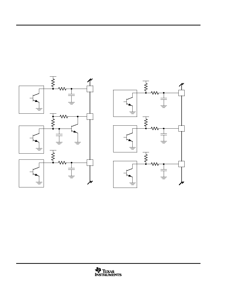
using the circuit shown in Figure 1.
In order to prevent noise from commanding improper commutation states, some form of low-pass filtering on
HALLA, HALLB, and HALLC is recommended. Passive RC networks generally work well and should be located
as close as possible to the device. Figure 2 illustrates these techniques.
HALLA
HALLB
HALLC
VREF
2N2222A
HALLA
HALLB
VREF
HALLC
1 k
499
1 k
1 k
499
1 k
2.2 nF
2.2 nF
2.2 nF
UDG≠97182
Figure 1. Converting Hall Code From 60
∞
to 120
∞
VREF
HALLA
HALLB
HALLC
VREF
HALLA
HALLB
VREF
HALLC
VREF
1 k
499
499
1 k
499
1 k
2.2 nF
2.2 nF
2.2 nF
UDG≠97185
Figure 2. Passive Hall Filtering Technique
UCC2626, UCC3626
SLUS318B ≠ APRIL 1999 ≠ REVISED JANUARY 2002
9
www.ti.com
APPLICATION INFORMATION
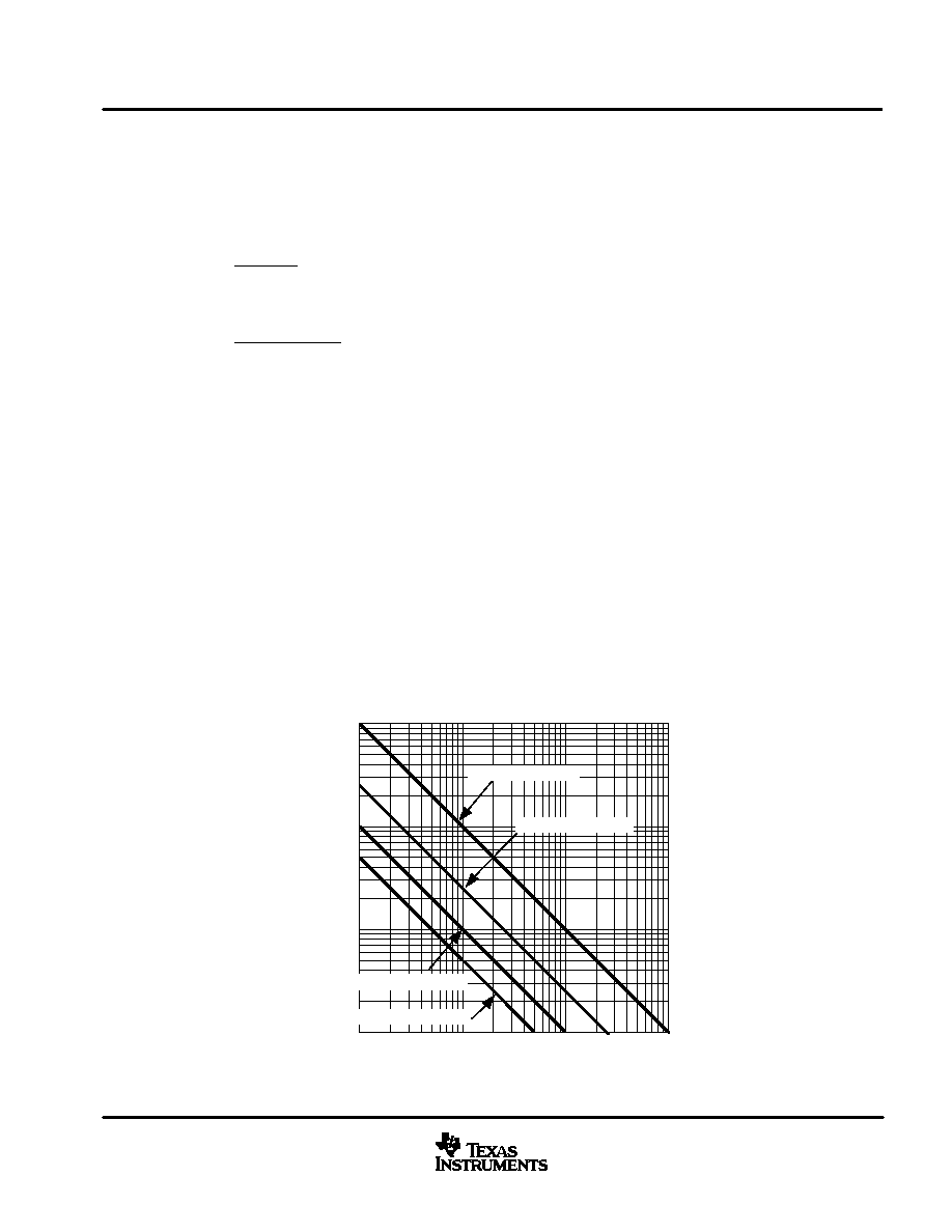
configuring the oscillator
The UCC3626 oscillator is designed to operate at frequencies up to 250 kHz and provide a triangle waveform
on CT with a peak-to-peak amplitude of 5 V for improved noise immunity. The current used to program CT is
derived from the R_TACH resistor according to the following equation:
I
OSC
+
25
R_TACH
Amps
The oscillator frequency is set by R_TACH and CT according to the following relationship:
f
OSC
+
2.5
R_TACH
CT
Hz
Timing resistor values should be between 25 k
and 500 k
,
while capacitor values should be between 100 pF
and 1
µ
F. Figure 3 provides a graph of oscillator frequency for various combinations of timing components. As
with any high-frequency oscillator, timing components should be located as close as possible to the device pins
when laying out the printed-circuit board. It is also important to reference the timing capacitor directly to the
ground pin on the UCC3626 rather than daisy chaining it to another trace or the ground plane. This technique
prevents switching current spikes in the local ground from causing jitter in the oscillator.
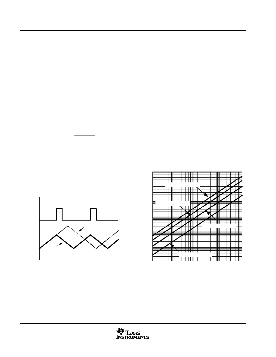
synchronizing the oscillator
A common system specification is to have all oscillators synchronized to a master clock. The UCC3626 provides
a SYNCH input for this purpose. The SYNCH input is designed to interface with a digital clock pulse generated
by the master oscillator. A positive-going edge on this input causes the UCC3626 oscillator to begin discharging.
In order for the slave oscillator to function properly, it must be programmed for a frequency slightly lower than
that of the master. Also, a resistor equal to R_TACH must be placed in parallel with CT. Figure 4 illustrates the
waveforms for a slave oscillator programmed to 20 kHz with a master frequency of 30 kHz. The SYNCH pin
must be grounded when not used.
Figure 3
1.E+03
1.E+04
1.E+05
1.E+06
1.E≠10
1.E≠09
1.E≠08
1.E≠07
R_TACH = 25 k
R_TACH = 100 k
R_TACH = 500 k
R_TACH = 250 k
CT ≠ Oscillator Timing Capacitance ≠ F
f OSC
≠
PWM Frequency
≠
Hz
OSCILLATOR FREQUENCY
vs
TIMING CAPACITANCE
(1)
(2)
UCC2626, UCC3626
SLUS318B ≠ APRIL 1999 ≠ REVISED JANUARY 2002
10
www.ti.com
APPLICATION INFORMATION
programming the tachometer
The UCC3626 tachometer consists of a precision 5-V monostable, triggered by either a rising or falling edge
on any of the three Hall inputs, HALLA, HALLB, and HALLC. The resulting TACH_OUT waveform is a variable
duty-cycle square wave whose frequency is proportional to motor speed, as given by:
TACH_OUT
+
V
P
20
Hz
where P is the number of motor pole pairs and V is motor velocity in RPM.
The on time of the monostable is programmed via timing resistor R_TACH and capacitor C_TACH according
to the following equation:
t
ON
+
R_TACH
C_TACH sec
Figure 5 provides a graph of on times for various combinations of R_TACH and C_TACH. On time is typically
set to a value less than the minimum TACH_OUT period as given by:
t
PERIOD (min)
+
20
V
MAX
P
sec
where P is the number of motor pole pairs and V is motor velocity in RPM.
SYNCH
CT
WITHOUT SYNCH
WITH SYNCH
Figure 4. Oscillator Waveforms
Figure 5
1.E≠06
1.E≠05
1.E≠04
1.E≠03
1.E≠02
1.E≠01
1.E+00
1.E≠10
1.E≠09
1.E≠08
1.E≠07
1.E≠06
R_TACH = 250 k
R_TACH = 25 k
R_TACH = 100 k
R_TACH = 500 k
t ON
≠
T
achometer On
≠
T
ime
≠
s
C_TACH ≠ Tachometer Timing Capacitance ≠ F
TACHOMETER ON-TIME
vs
TIMING CAPACITANCE
(3)
(4)
(5)
UCC2626, UCC3626
SLUS318B ≠ APRIL 1999 ≠ REVISED JANUARY 2002
11
www.ti.com
APPLICATION INFORMATION
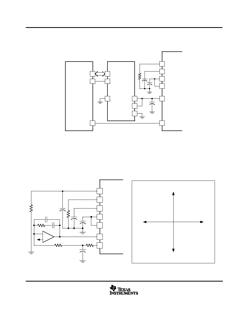
The TACH_OUT signal can be used to close a digital velocity loop using a microcontroller, as shown in Figure 6,
or directly low-pass filtered in an analog implementation, Figure 7.
UDG≠97188
5
4
14
R_TACH
C_TACH
PWM_NI
PWM_I
13
TACH_OUT
3
6
CT
UCC3626
VOUT
AD558
VCE
VCS
IC1
PC0
MC68HC11
PB0≠PB7
DB0≠DB7
VOUTSENSE
VOUTSELECT
Figure 6. Digital Velocity Loop Implementation Using MC68HC11
two quadrant vs four quadrant control
Figure 8 illustrates the four possible quadrants of operation for a motor. Two-quadrant control refers to a system
in which operation is limited to quadrants I and III (where torque and velocity are in the same direction). With
a two-quadrant brushless dc amplifier, there are no provisions other than friction to decelerate the load, limiting
the approach to less demanding applications. Four-quadrant controllers, on the other hand, provide controlled
operation in all quadrants, including II and IV, where torque and rotation are of opposite direction.
2
5
4
14
VREF
R_TACH
C_TACH
PWM_NI
PWM_I
13
TACH_OUT
3
6
CT
+
≠
UCC3626
Figure 7. Simple Analog Velocity Loop
UDG≠97189
I
IV
III
II
VELOCITY
CW
CCW
TORQUE
CW
CCW
UDG≠01118
Figure 8. Four Quadrants of Operation
UCC2626, UCC3626
SLUS318B ≠ APRIL 1999 ≠ REVISED JANUARY 2002
12
www.ti.com
APPLICATION INFORMATION
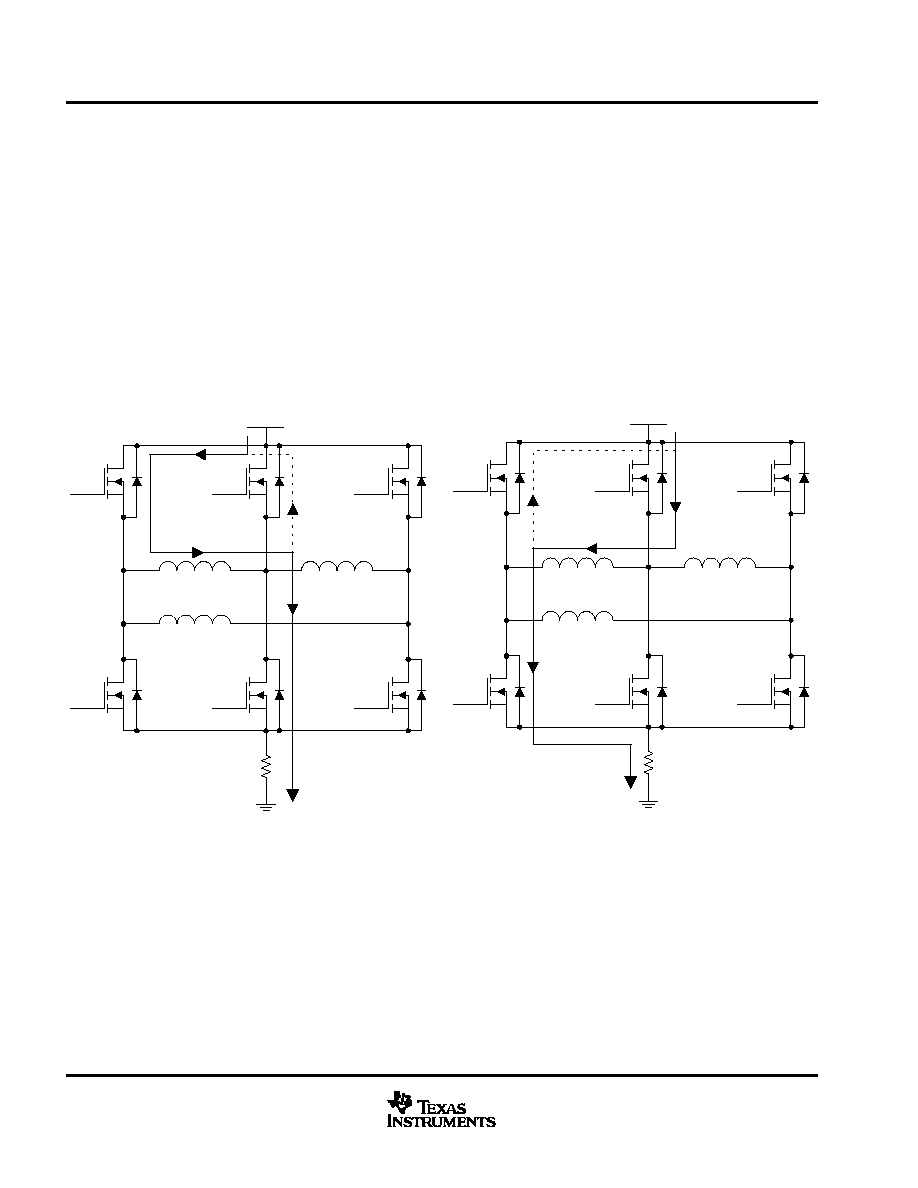
When configured for two-quadrant operation, (QUAD=0), the UCC3626 modulates only the low-side devices
of the output power stage. The current paths within the output stage during the PWM on- and off-times are
illustrated in Figure 9. During the on interval, both switches are on, and current flows through the load down to
ground. During the off time, the lower switch is shut off, and the motor current circulates through the upper half
bridge via the flyback diode. The motor is assumed to be operating in either quadrant I or III.
If operation is attempted in quadrants II or IV by changing the DIR bit and reversing the torque, switches 1 and
4 are turned off and switches 2 and 3 turned on. Under this condition motor current very quickly decays, reverses
direction and increases until the control threshold is reached. At this point, switch 2 turns off and current once
again circulates in the upper half bridge. However, in this case, the motor's BEMF is in phase with the current,
(i.e. the motor's direction of rotation has not yet changed.) Figure 10 illustrates the current paths when operating
in this mode. Under these conditions there is nothing to limit the current other than motor and drive impedance.
These high-circulating currents can result in damage to the power devices in addition to high, uncontrolled
torque.
Figure 9. Two-Quadrant Chopping
IPHASE
+ BEMF ≠
VMOT
IOFF
ION
S1
S3
S5
S2
S4
S6
UDG≠01119
Figure 10. Two-Quadrant Reversal
IPHASE
+ BEMF ≠
VMOT
IOFF
ION
S1
S3
S5
S2
S4
S6
UDG≠01120
UCC2626, UCC3626
SLUS318B ≠ APRIL 1999 ≠ REVISED JANUARY 2002
13
www.ti.com
APPLICATION INFORMATION
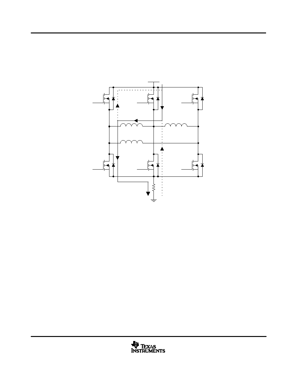
By pulse width modulating both the upper and lower power devices (QUAD=1), motor current always decays
during the PWM off time, eliminating any uncontrolled circulating currents. In addition, current always flows
through the current sense resistor, providing a suitable feedback signal. Figure 11 illustrates the current paths
during a four-quadrant torque reversal. Motor drive waveforms for both two- and four-quadrant operation are
illustrated in Figure 12.
UDG≠01121
IPHASE
+ BEMF ≠
VMOT
IOFF
ION
S1
S3
S5
S2
S4
S6
Figure 11. Four-Quadrant Reversal
UCC2626, UCC3626
SLUS318B ≠ APRIL 1999 ≠ REVISED JANUARY 2002
14
www.ti.com
APPLICATION INFORMATION
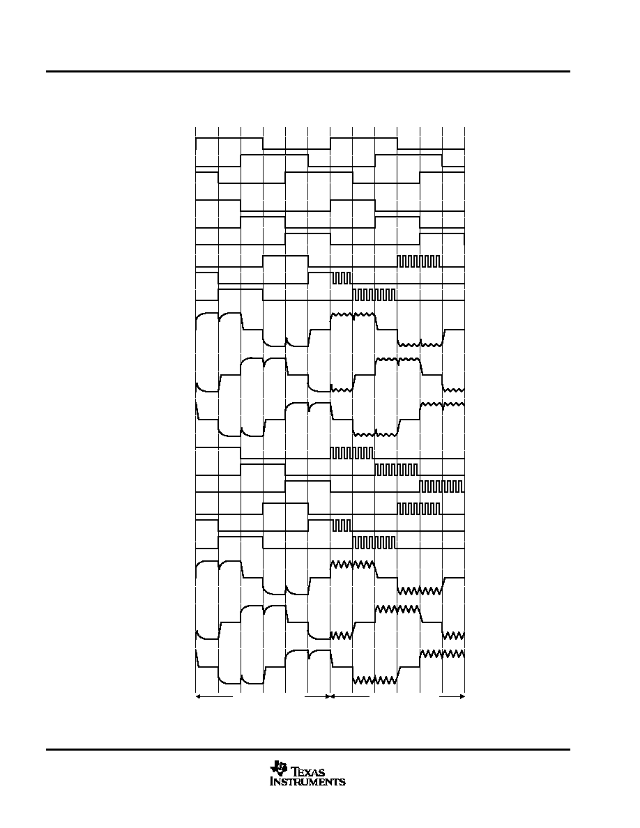
UDG≠97190
0
60
120
180
240
300
360
420
480
540
600
660
720
ROTOR POSITION IN ELECTRICAL DEGREES
Code
101
100
110
010
011
001
101
100
110
010
011
001
H1
H2
H3
AHI
BHI
CHI
ALO
BLO
CLO
+
0
≠
A
+
0
≠
B
+
0
≠
C
MOTOR
PHASE
CURRENTS
QUAD=0
LOW SIDE
OUTPUTS
QUAD=0
HIGH SIDE
OUTPUTS
QUAD=0
SENSOR
INPUTS
AHI
BHI
CHI
ALO
BLO
CLO
+
0
≠
A
+
0
≠
B
+
0
≠
C
MOTOR
PHASE
CURRENTS
QUAD=1
LOW SIDE
OUTPUTS
QUAD=1
HIGH SIDE
OUTPUTS
QUAD=1
100% Duty Cycle PWM
50% Duty Cycle PWM
Figure 12. Motor Drive and Current Waveforms for Two-Quadrant (QUAD=0)
and Four-Quadrant (QUAD=1) Operation
UCC2626, UCC3626
SLUS318B ≠ APRIL 1999 ≠ REVISED JANUARY 2002
15
www.ti.com
APPLICATION INFORMATION
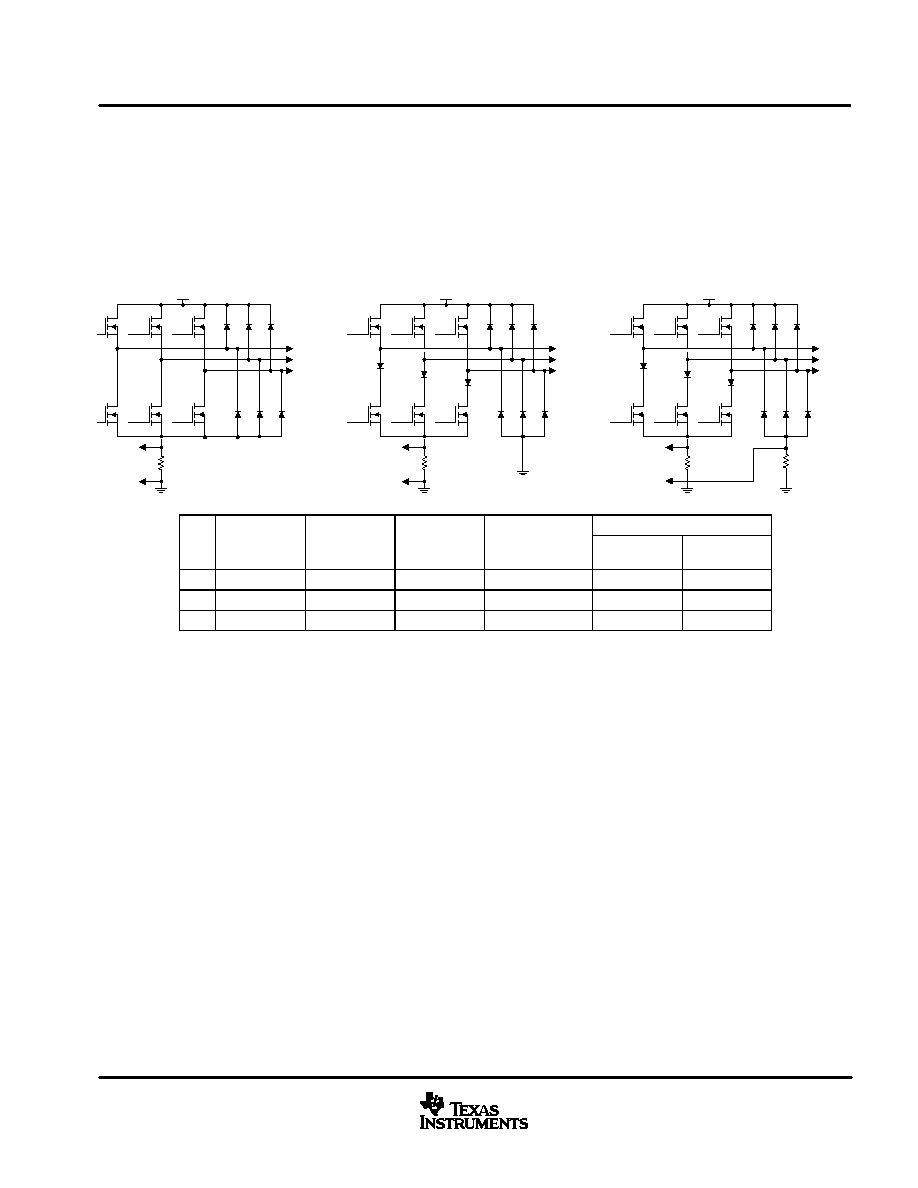
power stage design considerations
The flexible architecture of the UCC3626 requires the user to pay close attention to the design of the power
output stage. Two- and four-quadrant applications not requiring the brake function are able to use the power
stage approach illustrated in Figure 13a. In many cases the body diode of the MOSFET can be used to reduce
parts count and cost. If efficiency is a key requirement, Schottky diodes can be used in parallel with the switches.
UDG≠97190
(b)
(c)
TO
MOTOR
VMOT
CURRENT
SENSE
TO
MOTOR
VMOT
CURRENT
SENSE
TO
MOT
VMOT
CURRENT
SENSE
(a)
UDG≠01122
TWO
FOUR
SAFE
POWER
CURRENT SENSE
TWO
QUADRANT
FOUR
QUADRANT
SAFE
BRAKING
POWER
REVERSAL
PULSE-BY-
PULSE
AVERAGE
(a)
YES
YES
NO
Four-Quad Only
YES
YES
(b)
YES
NO
YES
No
YES
NO
(c)
YES
YES
YES
Four-Quad Only
YES
YES
Figure 13. Power Stage Topologies
If the system requires a braking function, diodes must be added in series with the lower power devices and the
lower flyback diodes must be returned to ground, as pictured in Figure 13b, and 13c. This requirement prevents
brake currents from circulating in the lower half bridge and bypassing the sense resistor. In addition, the
combination of braking and four-quadrant control necessitates an additional resistor in the diode path to sense
current during the PWM off time as illustrated in Figure 13c.

UCC2626, UCC3626
SLUS318B ≠ APRIL 1999 ≠ REVISED JANUARY 2002
16
www.ti.com
APPLICATION INFORMATION
current sensing
The UCC3626 includes a differential current-sense amplifier with a fixed gain of five, along with an absolute
value circuit. The current-sense signal should be low pass filtered to eliminate leading-edge spikes. In order to
maximize performance, the input impedance of the amplifier should be balanced. If the sense voltage must be
trimmed for accuracy reasons, a low-value input divider or a differential divider should be used to maintain
impedance matching, as shown in Figure 14.
UDG≠01123
RF
RADJ
RF
RS
CF
RF
RADJ
RF
RS
CF
SNS_NI
SNS_I
(a)
SNS_NI
SNS_I
(b)
RF
RADJ << RF
Figure 14. (a) Differential Divider and (b) Low-Value Divider
With four-quadrant chopping, motor current always flows through the sense resistor. However, during the
flyback period the polarity across the sense resistor is reversed. The absolute value amplifier cancels the
polarity reversal by inverting the negative sense signal during the flyback time, see Figure 15. Therefore, the
output of the absolute value amplifier is a reconstructed analog of the motor current, suitable for protection as
well as feedback loop closure.
UDG≠01124
IPHASE
+ BEMF ≠
VMOT
IOFF
ION
S1
S3
S5
S2
S4
S6
X5
Is
If
Im
Is
If
Im
Ip
Ip
5*Ip
Figure 15. Current Sense Amplifier Waveform
UCC2626, UCC3626
SLUS318B ≠ APRIL 1999 ≠ REVISED JANUARY 2002
17
www.ti.com
APPLICATION INFORMATION
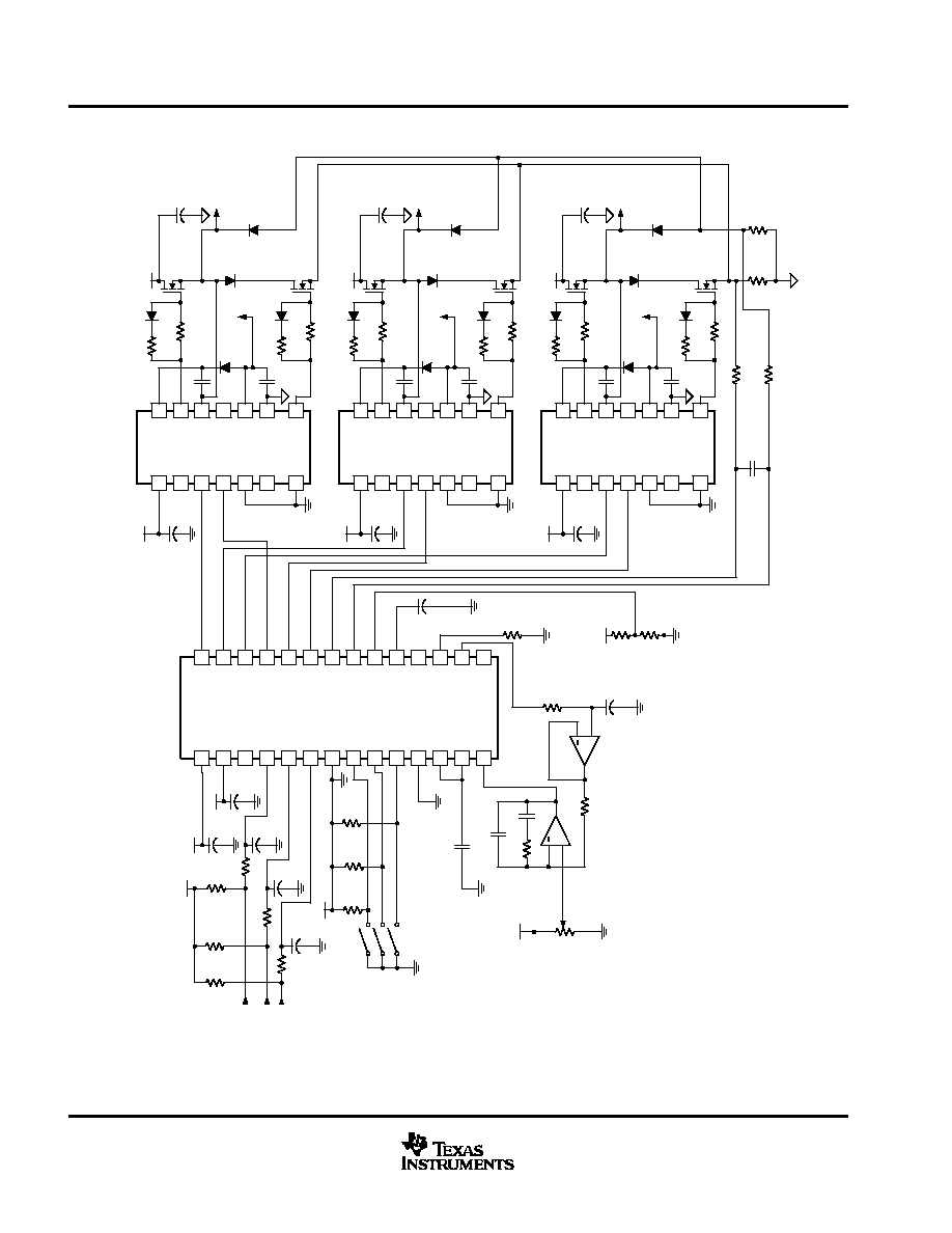
Figure 17 illustrates a simple 175-V, 2-A, two-quadrant velocity controller using the UCC3626. The power stage
is designed to operate with a rectified off-line supply using IR2210s to provide the interface between the low
voltage control signals and the power MOSFETs. The power topology illustrated in Figure 13c is implemented
in order to provide braking capability.
UDG≠99061
11
IOUT
+
≠
13
PWM_I
CURRENT
ERROR
AMPLIFIER
+
≠
U6
+
≠
SIGN/MAGNITUDE CONVERTER
21
DIR
U7
CURRENT SIGN
3
TACH_OUT
+
≠
U2
TACHOMETER
FILTER
2N7002
8
DIR_OUT
+
≠
U3
BIPOLAR
TACH GAIN
+
≠
U1
CURRENT
MAGNITUDE
U5
U8
10 k
10 k
10 k
10 k
10 k
10 k
4.99 k
4.99 k
10 k
VELOCITY
COMMAND
±
5 V
Figure 16. Four-Quadrant Control Loop
The controller's speed command is set by potentiometer R30, while the speed feedback signal is obtained by
low-pass filtering and buffering the TACH_OUT signal using R11 and C9. Small signal compensation of the
velocity control loop is provided by amplifier U5A, whose output is used to control the PWM duty cycle. The
integrating capacitor, C8, places a pole at 0 Hz and a zero in conjunction with R10. This zero can be used to
cancel the low-frequency motor pole and to cross the loop-over with a ≠20 dB gain response.
Four-quadrant applications require the control of motor current. Figure 16 illustrates a sign/magnitude current
control loop within an outer bipolar velocity loop using the UCC3626. U1 serves as the velocity loop error
amplifier and accepts a
±
5-V command signal. Velocity feedback is provided by low-pass filtering and scaling
the TACH_OUT signal using U2. The direction output switch, DIR_OUT, and U3 set the polarity of the
tachometer gain according to the direction of rotation. The output of the velocity error amplifier, U1, is then
converted to sign/magnitude form using U5 and U6. The sign portion is used to drive the DIR input while the
magnitude commands the current error amplifier, U8. Current feedback is provided by the internal current sense
amplifier via the IOUT pin.
UCC2626, UCC3626
SLUS318B ≠ APRIL 1999 ≠ REVISED JANUARY 2002
18
www.ti.com
APPLICATION INFORMATION
UDG≠01117
9
8
10
12
11
14
13
6
7
5
4
3
1
2
VDD
NC
HIN
LIN
SD
NC
VSS
VB
HO
VS
NC
VCC
LO
COM
U2
IR21
10
D16
1
1DF4
R18
47
R17
10
D2
1N4148
D7
MUR1520
+12V
D1
1N4148
R15
10
R16
47
D8
1N5418
Q2
IRF730
MOT
OR
PHASE A
VMOT
VREF
Q1
IRF730
28
2
1
15
16
17
20
27
25
23
26
24
9
22
VDD
VREF
GND
HALLA
HALLB
HALLC
QUAD
AHI
BHI
CHI
ALOW
BLOW
SNS_NI
CLOW
U1
UCC3626
10
11
8
5
12
SNS_I
IOUT
DIR_OUT
CT
ACH
OC_REF
3
4
T
ACH_OUT
R
T
ACH
21
19
18
6
7
13
14
DIR_IN
BRAKE
COAST
SYNCH
CT
PWN_IN
PWM_I
9
8
10
12
11
14
13
6
7
5
4
3
1
2
VDD
NC
HIN
LIN
SD
NC
VSS
VB
HO
VS
NC
VCC
LO
COM
U3
IR21
10
D17
1
1DF4
R22
47
R21
10
D4
1N4148
D10
MUR1520
+12V
D3
1N4148
R19
10
R20
47
D1
1
1N5418
Q4
IRF730
MOT
OR
PHASE B
VMOT
VREF
Q3
IRF730
9
8
10
12
11
14
13
6
7
5
4
3
1
2
VDD
NC
HIN
LIN
SD
NC
VSS
VB
HO
VS
NC
VCC
LO
COM
U3
IR21
10
D18
1
1DF4
R18
47
R25
10
D6
1N4148
D13
MUR1520
+12V
D5
1N4148
R23
10
R24
47
D15
1N5418
Q2
IRF730
MOT
OR
PHASE C
VMOT
VREF
Q5
IRF730
R30 2 k
R31 2 k
R13
35 k
VREF
R14
15 k
R12
250 k
C10
3900 pF
R1
1
160 k
+
U5B
1/2 LM358
R29
+
R10
C8
C7
C6
100 pF
R9
10 k
R8
10 k
R7
10 k
VREF
C5
2200 pF
C4
2200 pF
C3
2200 pF
C1
VREF
+12V
C2
SPEED SET
R30
10 k
VREF
R6
499
R5
499
R2
1 k
R4
499
R3
1 k
VREF
R1
1 k
FROM
HALL
SENSORS
R27
0.1
R28
0.1
0.1
µ
F
0.1
µ
F
C1
1
0.1
µ
F
C17
0.1
µ
F
C14
0.1
µ
F
C23
0.1
µ
F
C9
0.1
µ
F
C13
0.1
µ
F
C12
0.1
µ
F
C22
10
µ
F
C21
10
µ
F
C15
0.1
µ
F
C16
0.1
µ
F
C20
10
µ
F
C18
0.1
µ
F
C19
0.1
µ
F
U5A
1/2 LM358
Figure 17. Two-Quadrant Velocity Controller

IMPORTANT NOTICE
Texas Instruments Incorporated and its subsidiaries (TI) reserve the right to make corrections, modifications,
enhancements, improvements, and other changes to its products and services at any time and to discontinue
any product or service without notice. Customers should obtain the latest relevant information before placing
orders and should verify that such information is current and complete. All products are sold subject to TI's terms
and conditions of sale supplied at the time of order acknowledgment.
TI warrants performance of its hardware products to the specifications applicable at the time of sale in
accordance with TI's standard warranty. Testing and other quality control techniques are used to the extent TI
deems necessary to support this warranty. Except where mandated by government requirements, testing of all
parameters of each product is not necessarily performed.
TI assumes no liability for applications assistance or customer product design. Customers are responsible for
their products and applications using TI components. To minimize the risks associated with customer products
and applications, customers should provide adequate design and operating safeguards.
TI does not warrant or represent that any license, either express or implied, is granted under any TI patent right,
copyright, mask work right, or other TI intellectual property right relating to any combination, machine, or process
in which TI products or services are used. Information published by TI regarding third≠party products or services
does not constitute a license from TI to use such products or services or a warranty or endorsement thereof.
Use of such information may require a license from a third party under the patents or other intellectual property
of the third party, or a license from TI under the patents or other intellectual property of TI.
Reproduction of information in TI data books or data sheets is permissible only if reproduction is without
alteration and is accompanied by all associated warranties, conditions, limitations, and notices. Reproduction
of this information with alteration is an unfair and deceptive business practice. TI is not responsible or liable for
such altered documentation.
Resale of TI products or services with statements different from or beyond the parameters stated by TI for that
product or service voids all express and any implied warranties for the associated TI product or service and
is an unfair and deceptive business practice. TI is not responsible or liable for any such statements.
Mailing Address:
Texas Instruments
Post Office Box 655303
Dallas, Texas 75265
Copyright
2002, Texas Instruments Incorporated