 | –≠–ª–µ–∫—Ç—Ä–æ–Ω–Ω—ã–π –∫–æ–º–ø–æ–Ω–µ–Ω—Ç: UCC37322D | –°–∫–∞—á–∞—Ç—å:  PDF PDF  ZIP ZIP |
Document Outline
- FEATURES
- APPLICATIONS
- DESCRIPTION
- absolute maximum ratings over operating free-air temperature (unless otherwise noted)Å
- ordering information
- electrical characteristics, VDD = 4.5 V to 15 V, TA = -40∞C to 105∞C for UCC2732x, TA = 0∞C to 70∞C for UCC3732x, TA = TJ, (unless otherwise noted)
- input (IN)
- output (OUT)
- overall
- enable (ENBL)
- switching time(4)
- pin configurations
- power dissipation rating table
- terminal functions
- APPLICATION INFORMATION
- general information
- input stage
- output stage
- source/sink capabilities during miller plateau
- operational circuit layout
- VDD
- drive current and power requirements
- enable
- THERMAL INFORMATION
- references
- related products
- TYPICAL CHARACTERISTICS
- MECHANICAL DATA
- D (R-PDSO-G**) PLASTIC SMALL-OUTLINE PACKAGE
- DGN (MSOP) PowerPAD PLASTIC SMALL-OUTLINE PACKAGE
- P (PDIP) PLASTIC DUAL-IN-LINE
- IMPORTANT NOTICE

UCC27321, UCC27322
UCC37321, UCC37322
SLUS504C - SEPTEMBER 2002 - REVISED NOVEMBER 2004
SINGLE 9 A HIGH SPEED LOW-SIDE MOSFET DRIVER WITH ENABLE
1
www.ti.com
FEATURES
D
Industry-Standard Pin-Out With Addition of
Enable Funtion
D
High-Peak Current Drive Capability of
±
9 A at
the Miller Plateau Region Using TrueDrive
D
Efficient Constant Current Sourcing Using a
Unique BiPolar & CMOS Output Stage
D
TTL/CMOS Compatible Inputs Independent
of Supply Voltage
D
20-ns Typical Rise and Fall Times with 10-nF
Load
D
Typical Propagation Delay Times of 25 ns
With Input Falling and 35 ns with Input
Rising
D
4-V to 15-V Supply Voltage
D
Available in Thermally Enhanced MSOP
PowerPAD
TM
Package With 4.7
∞
C/W
jc
D
Rated From ≠40
∞
C to 105
∞
C
D
Pb-Free Finish (NiPdAu) on SOIC-8 and
PDIP-8 Packages
APPLICATIONS
D
Switch Mode Power Supplies
D
DC/DC Converters
D
Motor Controllers
D
Class-D Switching Amplifiers
D
Line Drivers
D
Pulse Transformer Driver
DESCRIPTION
The UCC37321/2 family of high-speed drivers
deliver 9 A of peak drive current in an industry
standard pinout. These drivers can drive the
largest of MOSFETs for systems requiring
extreme Miller current due to high dV/dt
transitions. This eliminates additional external
circuits and can replace multiple components to
reduce space, design complexity and assembly
cost. Two standard logic options are offered,
inverting (UCC37321) and noninverting
(UCC37322).
PowerPAD
t
is trademarks of Texas Instruments Incorporated.
PRODUCTION DATA information is current as of publication date.
Products conform to specifications per the terms of Texas Instruments
standard warranty. Production processing does not necessarily include
testing of all parameters.
Copyright
2004, Texas Instruments Incorporated
Please be aware that an important notice concerning availability, standard warranty, and use in critical applications of Texas Instruments
semiconductor products and disclaimers thereto appears at the end of this data sheet.
UDG-01112
1
OUT
VDD
IN
3
ENBL
7
VDD
8
INVERTING
NON-
INVERTING
PGND
6
OUT
5
4
AGND
VDD
2
INVERTING
UCC37321
0
0
0
0
1
0
0
1
1
1
1
0
NON-
INVERTING
UCC37322
0
0
0
0
1
0
0
0
1
1
1
1
ENBL
IN
OUT
INPUT/OUTPUT TABLE
RENBL
100 k
UCC27321, UCC27322
UCC37321, UCC37322
SLUS504C - SEPTEMBER 2002 - REVISED NOVEMBER 2004
2
www.ti.com
description (continued)
Using a design that inherently minimizes shoot-through current, the outputs of these can provide high gate drive
current where it is most needed at the Miller plateau region during the MOSFET switching transition. A unique
hybrid output stage paralleling bipolar and MOSFET transistors (TrueDrive) allows efficient current delivery at
low supply voltages. With this drive architecture, UCC37321/2/3 can be used in industry standard 6-A, 9-A and
many 12-A driver applications. Latch up and ESD protection circuitries are also included. Finally, the
UCC37321/2 provides an enable (ENBL) function to have better control of the operation of the driver
applications. ENBL is implemented on pin 3 which was previously left unused in the industry standard pin-out.
It is internally pulled up to Vdd for active high logic and can be left open for standard operation.
In addition to SOIC-8 (D) and PDIP-8 (P) package offerings, the UCC37321/2 also comes in the thermally
enhanced but tiny 8-pin MSOP PowerPAD
t
(DGN) package. The PowerPAD
t
package drastically lowers the
thermal resistance to extend the temperature operation range and improve the long-term reliability.
absolute maximum ratings over operating free-air temperature (unless otherwise noted)
}
UCCx732x
UNIT
Supply voltage, VDD
-0.3 to 16
V
Output current (OUT) DC, IOUT_DC
0.6
A
Input voltage (IN), VIN
-5 V to 6 V or VDD+0.3
(whichever is larger)
V
Enable voltage (ENBL)
-0.3 V to 6 V or VDD+0.3
(whichever is larger)
V
Power dissipation at TA = 25
∞
C
D package
650
mW
DGN package
3
W
P package
350
mW
Junction operating temperature, TJ
-55 to 150
∞
C
Storage temperature, Tstg
-65 to 150
∞
C
Lead temperature (soldering, 10 sec.)
300
∞
C
Stresses beyond those listed under "absolute maximum ratings" may cause permanent damage to the device. These are stress ratings only, and
functional operation of the device at these or any other conditions beyond those indicated under "recommended operating conditions" is not
implied. Exposure to absolute-maximum-rated conditions for extended periods may affect device reliability.
All voltages are with respect to GND. Currents are positive into, negative out of the specified terminal.
ordering information
OUTPUT
TEMPERATURE
PACKAGED DEVICES
OUTPUT
CONFIGURATION
TEMPERATURE
RANGE TA = TJ
SOIC-8 (D)
MSOP-8 PowerPAD
(DGN)
PDIP-8 (P)
Inverting
-40
∞
C to +105
∞
C
UCC27321D
UCC27321DGN
UCC27321P
Inverting
0
∞
C to +70
∞
C
UCC37321D
UCC37321DGN
UCC37321P
NonInverting
-40
∞
C to +105
∞
C
UCC27322D
UCC27322DGN
UCC27322P
NonInverting
0
∞
C to +70
∞
C
UCC37322D
UCC37322DGN
UCC37322P
D (SOIC-8) and DGN (PowerPAD-MSOP) packages are available taped and reeled. Add R suffix to device type (e.g.
UCC37321DR, UCC37322DGNR) to order quantities of 2,500 devices per reel.
UCC27321, UCC27322
UCC37321, UCC37322
SLUS504C - SEPTEMBER 2002 - REVISED NOVEMBER 2004
3
www.ti.com
electrical characteristics, V
DD
= 4.5 V to 15 V, T
A
= -40
∞
C to 105
∞
C for UCC2732x, T
A
= 0
∞
C to 70
∞
C
for UCC3732x, T
A
= T
J
, (unless otherwise noted)
input (IN)
PARAMETER
TEST CONDITION
MIN
TYP
MAX
UNITS
V
IN_H
, logic 1 input threshold
2
V
V
IN_L
, logic 0 input threshold
1
V
Input current
0 V
V
IN
V
DD
-10
0
10
µ
A
output (OUT)
PARAMETER
TEST CONDITION
MIN
TYP
MAX
UNITS
Peak output current(1)(2)
VDD = 14 V,
9
A
V
OH
, output high level
V
OH
= V
DD
≠ V
OUT
, I
OUT
= -10 mA
150
300
mV
V
OL
, output high level
I
OUT
= 10 mA
11
25
mV
Output resistance high(3)
I
OUT
= -10 mA,
V
DD
= 14 V
15
25
Output resistance low(3)
I
OUT
= 10 mA,
V
DD
= 14 V
1.1
2.5
latch-up protection(1)
500
mA
overall
PARAMETER
TEST CONDITION
MIN
TYP
MAX
UNITS
IN = LO, EN = LO,
VDD = 15 V
150
225
UCC37321
IN = HI, EN = LO,
VDD = 15 V
440
650
UCC37321
UCC27321
IN = LO, EN = HI,
VDD = 15 V
370
550
IDD, static operating current
UCC27321
IN = HI, EN = HI,
VDD = 15 V
370
550
A
IDD, static operating current
IN = LO, EN = LO,
VDD = 15 V
150
225
µ
A
UCC37322
IN = HI, EN = LO,
VDD = 15 V
450
650
UCC37322
UCC27322
IN = LO, EN = HI,
VDD = 15 V
75
125
UCC27322
IN = HI, EN = HI,
VDD = 15 V
675
1000
enable (ENBL)
PARAMETER
TEST CONDITION
MIN
TYP
MAX
UNITS
VIN_H, high-level input voltage
LO to HI transition
1.7
2.2
2.7
V
VIN_L, low-level input voltage
HI to LO transition
1.1
1.6
2.0
V
Hysteresis
0.25
0.55
0.90
V
RENBL, enable impedance
VDD = 14 V,
ENBL = GND
75
100
135
k
tD3, propagation delay time(5)
C
LOAD
= 10 nF
60
90
ns
tD4, propagation delay time(5)
C
LOAD
= 10 nF
60
90
ns
NOTES:
1. Ensured by design. Not tested in production.
2. The pullup / pulldown circuits of the driver are bipolar and MOSFET transistors in parallel. The peak output current rating is the
combined current from the bipolar and MOSFET transistors.
3. The pullup / pulldown circuits of the driver are bipolar and MOSFET transistors in parallel. The output resistance is the R
DS(ON)
of
the MOSFET transistor when the voltage on the driver output is less than the saturation voltage of the bipolar transistor.
5. See Figure 2.
UCC27321, UCC27322
UCC37321, UCC37322
SLUS504C - SEPTEMBER 2002 - REVISED NOVEMBER 2004
4
www.ti.com
electrical characteristics, V
DD
= 4.5 V to 15 V, T
A
= -40
∞
C to 105
∞
C for UCC2732x, T
A
= 0
∞
C to 70
∞
C
for UCC3732x, T
A
= T
J
, (unless otherwise noted) (continued)
switching time
(4)
PARAMETER
TEST CONDITION
MIN
TYP
MAX
UNITS
t
R
, rise time (OUT)
C
LOAD
= 10 nF
20
70
t
F
, fall time (OUT)
C
LOAD
= 10 nF
20
30
ns
t
D1
, propagation delay, IN rising (IN to OUT)
C
LOAD
= 10 nF
25
70
ns
t
D2
, propagation delay, IN falling (IN to OUT)
C
LOAD
= 10 nF
35
70
NOTES:
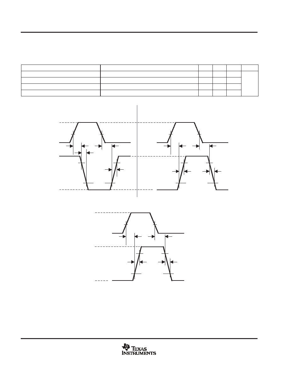
4. See Figure 1 for switching waveforms.
0V
5V
0V
IN
OUT
20%
80%
80%
20%
80%
80%
OUT
(a)
(b)
VTH
VTH
VDD
tD1
tD2
tF
tR
IN
VTH
tD1
tD2
tR
tF
VTH
Figure 1. Switching Waveforms for (a) Inverting Input to (b) Output Times
(6)
20%
80%
80%
VIN_H
VIN_L
tD3
tD4
tR
tF
0V
5V
0V
ENBL
OUT
VDD
Figure 2. Switching Waveform for Enable to Output
(6)
NOTES:
6. The 20% and 80% thresholds depict the dynamics of the BiPolar output devices that dominate the power MOSFET transition through
the Miller regions of operation.
UCC27321, UCC27322
UCC37321, UCC37322
SLUS504C - SEPTEMBER 2002 - REVISED NOVEMBER 2004
5
www.ti.com
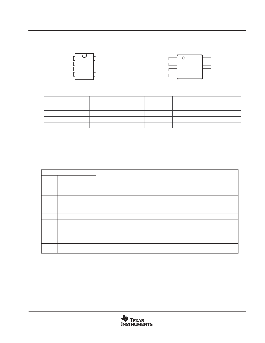
pin configurations
1
2
3
4
8
7
6
5
VDD
IN
ENBL
AGND
VDD
OUT
OUT
PGND
PDIP (P) PACKAGE
(TOP VIEW)
SOIC (D) OR MSOP (DGN) PACKAGE
(TOP VIEW)
VDD
OUT
OUT
PGND
8
7
6
5
1
2
3
4
VDD
IN
ENBL
AGND
power dissipation rating table
PACKAGE
SUFFIX
jc (
5
C/W)
ja (
5
C/W)
Power Rating
(mW)
TA = 70
5
C
Derating Factor
Above
70
5
C (mW/
5
C)
SOIC-8
D
42
84 ≠ 160
}
344-655
}
6.25 - 11.9
}
PDIP-8
P
49
110
500
9
MSOP PowerPAD-8
DGN
4.7
50-59
1370
17.1
125
∞
C operating junction temperature is used for power rating calculations
The range of values indicates the effect of pc-board. These values are intended to give the system designer an indication
of the best and worst case conditions. In general, the system designer should attempt to use larger traces on the pc-board
where possible in order to spread the heat away form the device more effectively. For additional information on device
temperature management, please refer to Packaging Information section of the Power Supply Control Products Data
Book, (Ti Literature Number SLUD003).
terminal functions
TERMINAL
FUNCTION
NO.
NAME
I/O
FUNCTION
4
AGND
-
Common ground for input stage. This ground should be connected very closely to the
source of the power MOSFET which the driver is driving. Grounds are separated to mini-
mize ringing affects due to output switching di/dt which can affect the input threshold.
3
ENBL
I
Enable input for the driver with logic compatible threshold and hysteresis. The driver output
can be enabled and disabled with this pin. It is internally pulled up to VDD with 100-k
resistor for active high operation. The output state when the device is disabled will be low
regardless of the input state.
2
IN
I
Input signal of the driver which has logic compatible threshold and hysteresis.
6, 7
OUT
O
Driver outputs that must be connected together externally. The output stage is capable of
providing 9-A peak drive current to the gate of a power MOSFET.
5
PGND
-
Common ground for output stage. This ground should be connected very closely to the
source of the power MOSFET which the driver is driving. Grounds are separated to mini-
mize ringing affects due to output switching di/dt which can affect the input threshold.
1, 8
VDD
I
Supply voltage and the power input connections for this device. Three pins must be con-
nected together externally.

UCC27321, UCC27322
UCC37321, UCC37322
SLUS504C - SEPTEMBER 2002 - REVISED NOVEMBER 2004
6
www.ti.com
APPLICATION INFORMATION
general information
The UCC37321 and UCC37322 drivers serve as an interface between low-power controllers and power
MOSFETs. They can also be used as an interface between DSPs and power MOSFETs. High-frequency power
supplies often require high-speed, high-current drivers such as the UCC37321/2 family. A leading application
is the need to provide a high power buffer stage between the PWM output of the control device and the gates
of the primary power MOSFET or IGBT switching devices. In other cases, the device drives the power device
gates through a drive transformer. Synchronous rectification supplies also have the need to simultaneously
drive multiple devices which can present an extremely large load to the control circuitry.
The inverting driver (UCC37321) is useful for generating inverted gate drive signals from controllers that have
only outputs of the
opposite
polarity. For example, this driver can provide a gate signal for ground referenced,
N-channel synchronous rectifier MOSFETs in buck derived converters. This driver can also be used for
generating a gate drive signal for a P-channel MOSFET from a controller that is designed for N-channel
applications.
MOSFET gate drivers are generally used when it is not feasible to have the primary PWM regulator device
directly drive the switching devices for one or more reasons. The PWM device may not have the brute drive
capability required for the intended switching MOSFET, limiting the switching performance in the application.
In other cases there may be a desire to minimize the effect of high frequency switching noise by placing the high
current driver physically close to the load. Also, newer devices that target the highest operating frequencies may
not incorporate onboard gate drivers at all. Their PWM outputs are only intended to drive the high impedance
input to a driver such as the UCC37321/2. Finally, the control device may be under thermal stress due to power
dissipation, and an external driver can help by moving the heat from the controller to an external package.
input stage
The IN threshold has a 3.3-V logic sensitivity over the full range of V
DD
voltages; yet, it is equally compatible
with 0 V to V
DD
signals. The inputs of UCC37321/2 family of drivers are designed to withstand
500-mA
reverse
current without either damage to the device or logic upset. In addition, the input threshold turn-off of the
UCC37321/2 has been slightly raised for improved noise immunity. The input stage of each driver should be
driven by a signal with a short rise or fall time. This condition is satisfied in typical power supply applications,
where the input signals are provided by a PWM controller or logic gates with fast transition times (<200 ns). The
IN input of the driver functions as a digital gate, and it is not intended for applications where a slow changing
input voltage is used to generate a switching output when the logic threshold of the input section is reached.
While this may not be harmful to the driver, the output of the driver may switch repeatedly at a high frequency.
Users should not attempt to shape the input signals to the driver in an attempt to slow down (or delay) the signal
at the output. If limiting the rise or fall times to the power device is desired, then an external resistance can be
added between the output of the driver and the load device, which is generally a power MOSFET gate. The
external resistor may also help remove power dissipation from the device package, as discussed in the section
on Thermal Considerations.
UCC27321, UCC27322
UCC37321, UCC37322
SLUS504C - SEPTEMBER 2002 - REVISED NOVEMBER 2004
7
www.ti.com
APPLICATION INFORMATION
output stage
The TrueDrive output stage is capable of supplying
±
9-A peak current pulses and swings to both VDD and GND
and can encourage even the most stubborn MOSFETs to switch. The pull-up/pull-down circuits of the driver are
constructed of bipolar and MOSFET transistors in parallel. The peak output current rating is the combined
current from the bipolar and MOSFET transistors. The output resistance is the R
DS(ON)
of the MOSFET
transistor when the voltage on the driver output is less than the saturation voltage of the bipolar transistor. Each
output stage also provides a very low impedance to overshoot and undershoot due to the body diode of the
external MOSFET. This means that in many cases, external-schottky-clamp diodes are not required.
This unique BiPolar and MOSFET hybrid output architecture (TrueDrive) allows efficient current sourcing at low
supply voltages. The UCC37321/2 family delivers 9 A of gate drive where it is most needed during the MOSFET
switching transition ≠ at the Miller plateau region ≠ providing improved efficiency gains.
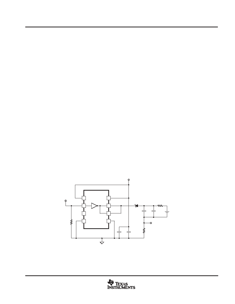
source/sink capabilities during miller plateau
Large power MOSFETs present a significant load to the control circuitry. Proper drive is required for efficient,
reliable operation. The UCC37321/2 drivers have been optimized to provide maximum drive to a power
MOSFET during the Miller Plateau Region of the switching transition. This interval occurs while the drain voltage
is swinging between the voltage levels dictated by the power topology, requiring the charging/discharging of the
drain-gate capacitance with current supplied or removed by the driver device.
[1]
Two circuits are used to test the current capabilities of the UCC37321/2 driver. In each case external circuitry
is added to clamp the output near 5 V while the device is sinking or sourcing current. An input pulse of 250 ns
is applied at a frequency of 1 kHz in the proper polarity for the respective test. In each test there is a transient
period where the current peaked up and then settled down to a steady-state value. The noted current
measurements are made at a time of 200 ns after the input pulse is applied, after the initial transient.
The circuit in Figure 3 is used to verify the current sink capability when the output of the driver is clamped around
5 V, a typical value of gate-source voltage during the Miller Plateau Region. The UCC37321 is found to sink 9 A
at V
DD
= 15 V.
UDG-01113
UCC37321
ENBL
1
2
3
4
AGND
IN
7
6
5
8
OUT
OUT
PGND
INPUT
1
µ
F
CER
100
µ
F
AL EL
DSCHOTTKY
VDD
C2
1
µ
F
VSNS
RSNS
0.1
C3
100
µ
F
10
+
VSUPPLY
5.5 V
VDD
VDD
Figure 3. Sink Current Test Circuit
UCC27321, UCC27322
UCC37321, UCC37322
SLUS504C - SEPTEMBER 2002 - REVISED NOVEMBER 2004
8
www.ti.com
APPLICATION INFORMATION
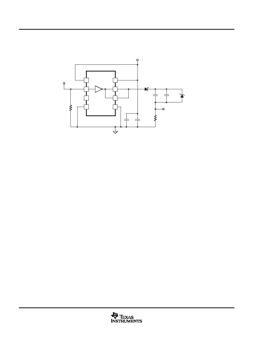
The circuit in Figure 4 is utilized to test the current source capability with the output clamped to around 5 V with
a string of Zener diodes. The UCC37321 is found to source 9 A at V
DD
= 15 V.
UDG-01114
UCC37321
ENBL
1
2
3
4
IN
7
6
5
8
OUT
OUT
INPUT
VDD
VDD
VDD
RSNS
0.1
VSNS
100
µ
F
AL EL
1
µ
F
CER
C2
1
µ
F
C3
100
µ
F
4.5 V
DADJ
DSCHOTTKY
AGND
PGND
Figure 4. Source Current Test Circuit
It should be noted that the current sink capability is slightly stronger than the current source capability at lower
VDD. This is due to the differences in the structure of the bipolar-MOSFET power output section, where the
current source is a P-channel MOSFET and the current sink has an N-channel MOSFET.
In a large majority of applications it is advantageous that the turn-off capability of a driver is stronger than the
turn-on capability. This helps to ensure that the MOSFET is held OFF during common power supply transients
which may turn the device back ON.
operational circuit layout
It can be a significant challenge to avoid the overshoot/undershoot and ringing issues that can arise from circuit
layout. The low impedance of these drivers and their high di/dt can induce ringing between parasitic inductances
and capacitances in the circuit. Utmost care must be used in the circuit layout.
In general, position the driver physically as close to its load as possible. Place a 1-
µ
F bypass capacitor as close
to the output side of the driver as possible, connecting it to pins 1 and 8. Connect a single trace between the
two VDD pins (pin 1 and pin 8); connect a single trace between PGND and AGND (pin 5 and pin 4). If a ground
plane is used, it may be connected to AGND; do not extend the plane beneath the output side of the package
(pins 5 - 8). Connect the load to both OUT pins (pins 7 and 6) with a single trace on the adjacent layer to the
component layer; route the return current path for the output on the component side, directly over the output
path.
Extreme conditions may require decoupling the input power and ground connections from the output power and
ground connections. The UCCx7321/2 has a feature that allows the user to take these extreme measures, if
necessary. There is a small amount of internal impedance of about 15
between the AGND and PGND pins;
there is also a small amount of impedance (
30
) between the two VDD pins. In order to take advantage of
this feature, connect a 1-
µ
F bypass capacitor between VDD and PGND (pins 5 and 8) and connect a 0.1-
µ
F
bypass capacitor between VDD and AGND (pins 1 and 4). Further decoupling can be achieved by connecting
between the two VDD pins with a jumper that passes through a 40-MHz ferrite bead and connect bias power
only to pin 8. Even more decoupling can be achieved by connecting between AGND and PGND with a pair of
anti-parallel diodes (anode connected to cathode and cathode connected to anode).

UCC27321, UCC27322
UCC37321, UCC37322
SLUS504C - SEPTEMBER 2002 - REVISED NOVEMBER 2004
9
www.ti.com
APPLICATION INFORMATION
VDD
Although quiescent VDD current is very low, total supply current will be higher, depending on OUTA and OUTB
current and the operating frequency. Total VDD current is the sum of quiescent VDD current and the average
OUT current. Knowing the operating frequency and the MOSFET gate charge (Qg), average OUT current can
be calculated from:
I
OUT
= Qg x f, where f is frequency
For the best high-speed circuit performance, two V
DD
bypass capacitors are recommended tp prevent noise
problems. The use of surface mount components is highly recommended. A 0.1-
µ
F ceramic capacitor should
be located closest to the VDD to ground connection. In addition, a larger capacitor (such as 1-
µ
F) with relatively
low ESR should be connected in parallel, to help deliver the high current peaks to the load. The parallel
combination of capacitors should present a low impedance characteristic for the expected current levels in the
driver application.
drive current and power requirements
The UCC37321/2 family of drivers are capable of delivering 9-A of current to a MOSFET gate for a period of
several hundred nanoseconds. High peak current is required to turn an N-channel device ON quickly. Then, to
turn the device OFF, the driver is required to sink a similar amount of current to ground. This repeats at the
operating frequency of the power device. An N-channel MOSFET is used in this discussion because it is the
most common type of switching device used in high frequency power conversion equipment.
References 1 and 2 contain detailed discussions of the drive current required to drive a power MOSFET and
other capacitive-input switching devices. Much information is provided in tabular form to give a range of the
current required for various devices at various frequencies. The information pertinent to calculating gate drive
current requirements will be summarized here; the original document is available from the TI website.
When a driver device is tested with a discrete, capacitive load it is a fairly simple matter to calculate the power
that is required from the bias supply. The energy that must be transferred from the bias supply to charge the
capacitor is given by:
E
+
1
2
CV2, where C is the load capacitor and V is the bias voltage feeding the driver.
There is an equal amount of energy transferred to ground when the capacitor is discharged. This leads to a
power loss given by the following:
P
+
2
1
2
CV2f, where f is the switching frequency.
This power is dissipated in the resistive elements of the circuit. Thus, with no external resistor between the driver
and gate, this power is dissipated inside the driver. Half of the total power is dissipated when the capacitor is
charged, and the other half is dissipated when the capacitor is discharged. An actual example using the
conditions of the previous gate drive waveform should help clarify this.
With V
DD
= 12 V, C
LOAD
= 10 nF, and f = 300 kHz, the power loss can be calculated as:
P = 10 nF x (12)
2
x (300 kHz) = 0.432 W
With a 12-V supply, this would equate to a current of:
I
+
P
V
+
0.432 W
12 V
+
0.036 A
UCC27321, UCC27322
UCC37321, UCC37322
SLUS504C - SEPTEMBER 2002 - REVISED NOVEMBER 2004
10
www.ti.com
APPLICATION INFORMATION
drive current and power requirements (continued)
The switching load presented by a power MOSFET can be converted to an equivalent capacitance by examining
the gate charge required to switch the device. This gate charge includes the effects of the input capacitance
plus the added charge needed to swing the drain of the device between the ON and OFF states. Most
manufacturers provide specifications that provide the typical and maximum gate charge, in nC, to switch the
device under specified conditions. Using the gate charge Qg, one can determine the power that must be
dissipated when charging a capacitor. This is done by using the equivalence Qg = CeffV to provide the following
equation for power:
P
+
C
V2
f
+
Qg
V
f
This equation allows a power designer to calculate the bias power required to drive a specific MOSFET gate
at a specific bias voltage.
enable
UCC37321/2 provides an Enable input for improved control of the driver operation. This input also incorporates
logic compatible thresholds with hysteresis. It is internally pulled up to V
DD
with 100-k
resistor for active high
operation. When ENBL is high, the device is enabled and when ENBL is low, the device is disabled. The default
state of the ENBL pin is to enable the device and therefore can be left open for standard operation. The output
state when the device is disabled is low regardless of the input state. See the truth table below for the operation
using enable logic.
ENBL input is compatible with both logic signals and slow changing analog signals. It can be directly driven or
a power-up delay can be programmed with a capacitor between ENBL and AGND.
Table 1. Input/Ouput Table
INVERTING
UCC37321
0
0
0
0
1
0
0
1
1
1
1
0
NON-
INVERTING
UCC37322
0
0
0
0
1
0
0
0
1
1
1
1
ENBL
IN
OUT
UCC27321, UCC27322
UCC37321, UCC37322
SLUS504C - SEPTEMBER 2002 - REVISED NOVEMBER 2004
11
www.ti.com
THERMAL INFORMATION
The useful range of a driver is greatly affected by the drive power requirements of the load and the thermal
characteristics of the device package. In order for a power driver to be useful over a particular temperature range
the package must allow for the efficient removal of the heat produced while keeping the junction temperature
within rated limits. The UCC37321/2 family of drivers is available in three different packages to cover a range
of application requirements.
As shown in the power dissipation rating table, the SOIC-8 (D) and PDIP-8 (P) packages each have a power
rating of around 0.5 W with T
A
= 70
∞
C. This limit is imposed in conjunction with the power derating factor also
given in the table. Note that the power dissipation in our earlier example is 0.432 W with a 10-nF load, 12 VDD,
switched at 300 kHz. Thus, only one load of this size could be driven using the D or P packag. The difficulties
with heat removal limit the drive available in the D or P packages.
The MSOP PowerPAD-8 (DGN) package significantly relieves this concern by offering an effective means of
removing the heat from the semiconductor junction. As illustrated in Reference 3, the PowerPAD packages offer
a leadframe die pad that is exposed at the base of the package. This pad is soldered to the copper on the PC
board directly underneath the device package, reducing the
jc down to 4.7
∞
C/W. Data is presented in
Reference 3 to show that the power dissipation can be quadrupled in the PowerPAD configuration when
compared to the standard packages. The PC board must be designed with thermal lands and thermal vias to
complete the heat removal subsystem, as summarized in Reference 4. This allows a significant improvement
in heatsinking over that available in the D or P packages, and is shown to more than double the power capability
of the D and P packages.
Note that the PowerPAD
t
is not directly connected to any leads of the package. However, it is electrically and
thermally connected to the substrate which is the ground of the device.
references
1.
SEM-1400, Topic 2, A Design and Application Guide for High Speed Power MOSFET Gate Drive Circuits,
TI Literature No. SLUP133
2.
U-137, Practical Considerations in High Performance MOSFET, IGBT and MCT Gate Drive Circuits, by Bill
Andreycak, TI Literature No. SLUA105
3.
Technical Brief, PowerPad Thermally Enhanced Package, TI Literature No. SLMA002
4.
Application Brief, PowerPAD Made Easy, TI Literature No. SLMA004
related products
PRODUCT
DESCRIPTION
PACKAGES
UCC37323/4/5
Dual 4-A Low-Side Drivers
MSOP-8 PowerPAD, SOIC-8, PDIP-8
UCC27423/4/5
Dual 4-A Low-Side Drivers with Enable
MSOP-8 PowerPAD, SOIC-8, PDIP-8
TPS2811/12/13
Dual 2-A Low-Side Drivers with Internal Regulator
TSSOP-8, SOIC-8, PDIP-8
TPS2814/15
Dual 2-A Low-Side Drivers with Two Inputs per Channel
TSSOP-8, SOIC-8, PDIP-8
TPS2816/17/18/19
Single 2-A Low-Side Driver with Internal Regulator
5-Pin SOT-23
TPS2828/29
Single 2-A Low-Side Driver
5-Pin SOT-23
UCC27321, UCC27322
UCC37321, UCC37322
SLUS504C - SEPTEMBER 2002 - REVISED NOVEMBER 2004
12
www.ti.com
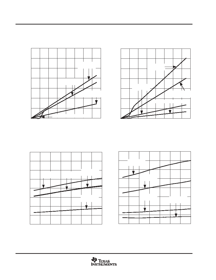
TYPICAL CHARACTERISTICS
Figure 5
INPUT CURRENT IDLE
vs
SUPPLY VOLTAGE (UCCx7321)
I DD
- Input Current Idle -
µ
A
VDD - Supply Voltage - V
600
700
400
500
100
200
300
0
0
16
2
4
6
8
14
12
10
ENBL = VDD
IN = 5 V
ENBL = 0 V
IN = 0 V
ENBL = VDD, IN = 0 V
ENBL = 0 V
IN = 5 V
600
700
400
500
100
200
300
0
0
16
2
4
6
8
14
12
10
INPUT CURRENT IDLE
vs
SUPPLY VOLTAGE (UCCx7322)
I DD
- Input Current Idle -
µ
A
VDD - Supply Voltage - V
ENBL = 0 V
IN = 0 V
ENBL = 0 V
IN = 5 V
Figure 6
ENBL = VDD
IN = 5 V
ENBL = VDD, IN = 0 V
Figure 7
INPUT CURRENT IDLE
vs
TEMPERATURE (UCCx7321)
I DD
- Input Current Idle -
µ
A
TJ -Temperature -
∞
C
600
700
400
800
500
100
200
300
0
-50
125
-25
0
25
50
100
75
ENBL = LO
IN = HI
ENBL = HI
IN = HI
ENBL = LO
IN = LO
ENBL = HI
IN = LO
Figure 8
INPUT CURRENT IDLE
vs
TEMPERATURE (UCCx7322)
I DD
- Input Current Idle -
µ
A
TJ -Temperature -
∞
C
600
700
400
800
500
100
200
300
0
-50
125
-25
0
25
50
100
75
ENBL = LO
IN = HI
ENBL = HI
IN = HI
ENBL = LO
IN = LO
ENBL = HI
IN = LO
UCC27321, UCC27322
UCC37321, UCC37322
SLUS504C - SEPTEMBER 2002 - REVISED NOVEMBER 2004
13
www.ti.com
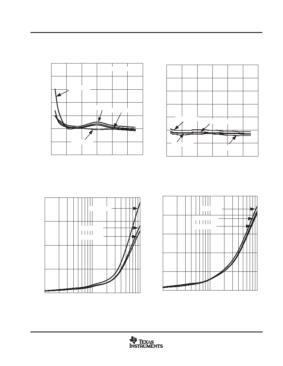
TYPICAL CHARACTERISTICS
Figure 9
0
10
20
30
40
50
60
70
4
16
6
8
10
14
12
RISE TIME
vs
SUPPLY VOLTAGE
t R
- Rise T
ime - ns
VDD - Supply Voltage - V
tA = -40
∞
C
tA = 105
∞
C
tA = 25
∞
C
tA = 0
∞
C
CLOAD = 10 nF
Figure 10
0
10
20
30
40
50
60
70
4
16
6
8
10
14
12
tA = -40
∞
C
tA = 105
∞
C
tA = 25
∞
C
tA = 0
∞
C
t F
- Fall T
ime - ns
VDD - Supply Voltage - V
FALL TIME
vs
SUPPLY VOLTAGE
Figure 11
RISE TIME
vs
LOAD CAPACITANCE
t R
- Rise T
ime - ns
CLOAD - Load Capacitance - nF
0
10
20
30
40
1
10
100
VDD = 5 V
VDD = 10 V
VDD = 15 V
Figure 12
FALL TIME
vs
OUTPUT CAPACITANCE
t F
- Fall T
ime - ns
CLOAD - Load Capacitance - nF
40
80
120
160
200
0
1
10
100
VDD = 5 V
VDD = 10 V
VDD = 15 V
UCC27321, UCC27322
UCC37321, UCC37322
SLUS504C - SEPTEMBER 2002 - REVISED NOVEMBER 2004
14
www.ti.com
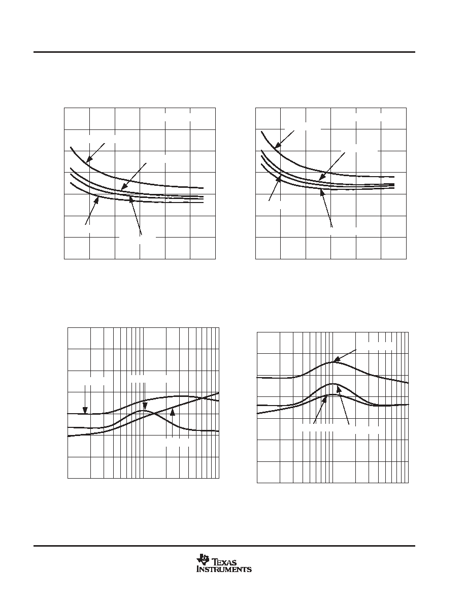
TYPICAL CHARACTERISTICS
10
20
40
50
60
0
30
70
4
16
6
8
10
14
12
Figure 13
t
D1
DELAY TIME
vs
SUPPLY VOLTAGE
t D1
- Delay T
ime - ns
VDD - Supply Voltage - V
tA = -40
∞
C
tA = 105
∞
C
tA = 25
∞
C
tA = 0
∞
C
CLOAD = 10 nF
10
20
40
50
60
0
30
70
4
16
6
8
10
14
12
Figure 14
t
D2
DELAY TIME
vs
SUPPLY VOLTAGE
t D2
- Delay T
ime - ns
VDD - Supply Voltage - V
tA = -40
∞
C
tA = 105
∞
C
tA = 0
∞
C
CLOAD = 10 nF
tA = 25
∞
C
10
30
40
60
70
0
1
10
100
20
50
Figure 15
t
D1
DELAY TIME
vs
LOAD CAPACITANCE
CLOAD - Load Capacitance - nF
t D1
- Delay T
ime - ns
VDD = 5 V
VDD = 15 V
VDD = 10 V
70
10
100
10
30
40
60
0
1
20
50
Figure 16
t
D2
DELAY TIME
vs
LOAD CAPACITANCE
CLOAD - Load Capacitance - nF
t D2
- Delay T
ime - ns
VDD = 15 V
VDD = 5 V
VDD = 10 V

UCC27321, UCC27322
UCC37321, UCC37322
SLUS504C - SEPTEMBER 2002 - REVISED NOVEMBER 2004
15
www.ti.com
TYPICAL CHARACTERISTICS
Figure 17
PROPAGATION TIMES
vs
PEAK INPUT VOLTAGE
Propagation
T
ime - ns
tD2
VIN(peak) - Peak Input Voltage - V
30
40
45
25
50
35
0
10
15
20
5
15
0
10
5
tRISE
tFALL
tD1
VDD = 15 V
CLOAD = 10 nF
TA = 25
∞
C
Figure 18
-50
1.2
1.3
1.4
1.5
1.6
1.7
1.8
1.9
2.0
125
-25
0
25
50
100
75
INPUT THRESHOLD
vs
TEMPERATURE
V
ON
- Input Threshold V
o
ltage - V
TJ - Temperature -
∞
C
VDD = 15 V
VDD = 10 V
VDD = 4.5 V
1.0
1.5
2.0
2.5
3.0
0
0.5
-50
125
-25
0
25
50
100
75
ENABLE THRESHOLD AND HYSTERESIS
vs
TEMPERATURE
TJ - Temperature -
∞
C
Enable threshold and hysteresis - V
Figure 19
ENBL - ON
ENBL - OFF
ENBL - HYSTERESIS
Figure 20
ENABLE RESISTANCE
vs
TEMPERATURE
R
ENBL
- Enable Resistance -
TJ - Temperature -
∞
C
110
130
140
100
150
120
70
80
90
60
-50
125
-25
0
25
50
100
75
50
UCC27321, UCC27322
UCC37321, UCC37322
SLUS504C - SEPTEMBER 2002 - REVISED NOVEMBER 2004
16
www.ti.com
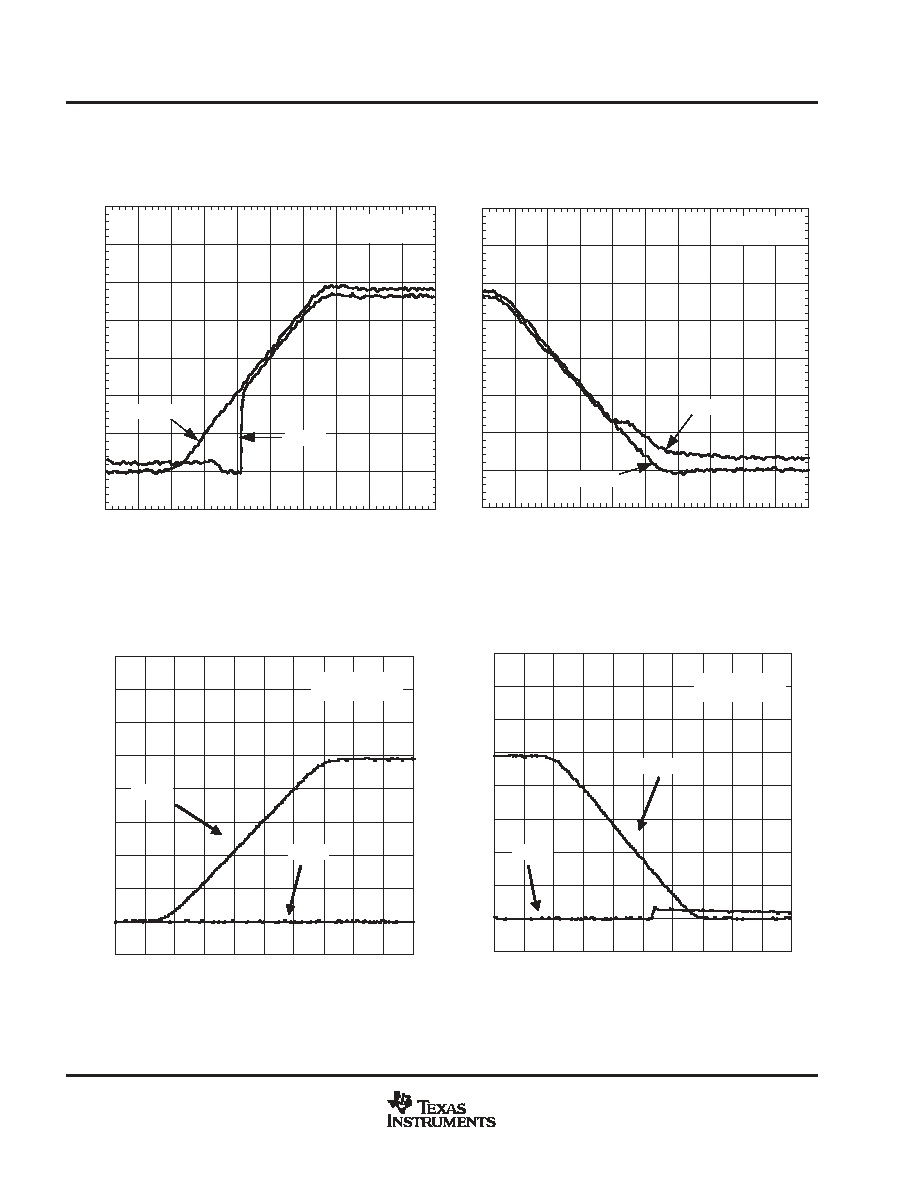
TYPICAL CHARACTERISTICS
OUTPUT BEHAVIOR
vs
V
DD
(UCC37321)
10 nF Between Output and GND
50
µ
s/div
Figure 21
V
DD
- Input V
o
ltage - V
1 V/div
OUT
VDD
IN = GND
ENBL = VDD
0 V
Figure 22
10 nF Between Output and GND
50
µ
s/div
V
DD
- Input V
oltage - V
1 V/div
OUTPUT BEHAVIOR
vs
V
DD
(UCC37321)
VDD
OUT
IN = GND
ENBL = VDD
0 V
Figure 23
10 nF Between Output and GND
50
µ
s/div
V
DD
- Supply V
o
ltage - V
1 V/div
OUT
VDD
0 V
OUTPUT BEHAVIOR
vs
VDD (INVERTING)
IN = VDD
ENBL = VDD
Figure 24
OUTPUT BEHAVIOR
vs
VDD (INVERTING)
10 nF Between Output and GND
50
µ
s/div
V
DD
- Supply V
oltage - V
1 V/div
OUT
VDD
0 V
IN = VDD
ENBL = VDD

UCC27321, UCC27322
UCC37321, UCC37322
SLUS504C - SEPTEMBER 2002 - REVISED NOVEMBER 2004
17
www.ti.com
TYPICAL CHARACTERISTICS
OUTPUT BEHAVIOR
vs
VDD (UCC37322)
10 nF Between Output and GND
50
µ
s/div
Figure 25
V
DD
- Input V
o
ltage - V
1 V/div
OUT
VDD
IN = VDD
ENBL = VDD-
IN = GND
0 V
Figure 26
10 nF Between Output and GND
50
µ
s/div
V
DD
- Input V
o
ltage - V
1 V/div
OUTPUT BEHAVIOR
vs
VDD (UCC37322)
OUT
VDD
IN = VDD
ENBL = VDD-
IN = GND
0 V
Figure 27
10 nF Between Output and GND
50
µ
s/div
V
DD
- Supply V
o
ltage - V
1 V/div
0 V
OUTPUT BEHAVIOR
vs
VDD (NON-INVERTING)
VDD
OUT
IN = GND
ENBL = VDD
Figure 28
OUTPUT BEHAVIOR
vs
VDD (NON-INVERTING)
10 nF Between Output and GND
50
µ
s/div
V
DD
- Supply V
o
ltage - V
1 V/div
0 V
VDD
OUT
IN = GND
ENBL = VDD

UCC27321, UCC27322
UCC37321, UCC37322
SLUS504C - SEPTEMBER 2002 - REVISED NOVEMBER 2004
18
www.ti.com
MECHANICAL DATA
D (R-PDSO-G**)
PLASTIC SMALL-OUTLINE PACKAGE
8 PINS SHOWN
8
0.197
(5,00)
A MAX
A MIN
(4,80)
0.189
0.337
(8,55)
(8,75)
0.344
14
0.386
(9,80)
(10,00)
0.394
16
DIM
PINS **
4040047/E 09/01
0.069 (1,75) MAX
Seating Plane
0.004 (0,10)
0.010 (0,25)
0.010 (0,25)
0.016 (0,40)
0.044 (1,12)
0.244 (6,20)
0.228 (5,80)
0.020 (0,51)
0.014 (0,35)
1
4
8
5
0.150 (3,81)
0.157 (4,00)
0.008 (0,20) NOM
0
∞
- 8
∞
Gage Plane
A
0.004 (0,10)
0.010 (0,25)
0.050 (1,27)
NOTES: A. All linear dimensions are in inches (millimeters).
B. This drawing is subject to change without notice.
C. Body dimensions do not include mold flash or protrusion, not to exceed 0.006 (0,15).
D. Falls within JEDEC MS-012

UCC27321, UCC27322
UCC37321, UCC37322
SLUS504C - SEPTEMBER 2002 - REVISED NOVEMBER 2004
19
www.ti.com
MECHANICAL DATA
DGN (MSOP)
PowerPAD
PLASTIC SMALL-OUTLINE PACKAGE
0,69
0,41
0,25
Thermal Pad
(See Note F)
0,15 NOM
Gage Plane
4073271/A 04/98
4,98
0,25
5
3,05
4,78
2,95
8
4
3,05
2,95
1
0,38
0,15
0,05
1,07 MAX
Seating Plane
0,10
0,65
M
0,25
0
∞
- 6
∞
NOTES: A. All linear dimensions are in millimeters.
B. This drawing is subject to change without notice.
C. Body dimensions include mold flash or protrusions.
D. The package thermal performance may be enhanced by attaching an external heat sink to the thermal pad.
This pad is electrically and thermally connected to the backside of the die.
E. Falls within JEDEC MO-187
F.
The PowerPAD
is not directly connected to any leads of the package. However, it is electrically and thermally connected to the
substrate which is the ground of the device. The exposed pad dimension is 1.3 mm x 1.7 mm. However, the tolerances can be
+1.05/-0.05 mm (+ 41 / -2 mils) due to position and mold flow variation.
G.
For additional information on the PowerPAD
t
package and how to take advantage of its heat dissipating abilities, refer to Technical
Brief, PowerPad Thermally Enhanced Package, Texas Instrument s Literature No. SLMA002 and Application Brief, PowerPad Made
Easy, Texas Instruments Literature No. SLMA004. Both documents are available at www.ti.com.
PowerPAD is a trademark of Texas Instruments Incorporated.

UCC27321, UCC27322
UCC37321, UCC37322
SLUS504C - SEPTEMBER 2002 - REVISED NOVEMBER 2004
20
www.ti.com
MECHANICAL DATA
P (PDIP)
PLASTIC DUAL-IN-LINE
8
4
0.015 (0,38)
Gage Plane
0.325 (8,26)
0.300 (7,62)
0.010 (0,25) NOM
MAX
0.430 (10,92)
4040082/D 05/98
0.200 (5,08) MAX
0.125 (3,18) MIN
5
0.355 (9,02)
0.020 (0,51) MIN
0.070 (1,78) MAX
0.240 (6,10)
0.260 (6,60)
0.400 (10,60)
1
0.015 (0,38)
0.021 (0,53)
Seating Plane
M
0.010 (0,25)
0.100 (2,54)
NOTES: A. All linear dimensions are in inches (millimeters).
B. This drawing is subject to change without notice.
C. Falls within JEDEC MS-001
For the latest package information, go to http://www.ti.com/sc/docs/package/pkg_info.htm

IMPORTANT NOTICE
Texas Instruments Incorporated and its subsidiaries (TI) reserve the right to make corrections, modifications,
enhancements, improvements, and other changes to its products and services at any time and to discontinue
any product or service without notice. Customers should obtain the latest relevant information before placing
orders and should verify that such information is current and complete. All products are sold subject to TI's terms
and conditions of sale supplied at the time of order acknowledgment.
TI warrants performance of its hardware products to the specifications applicable at the time of sale in
accordance with TI's standard warranty. Testing and other quality control techniques are used to the extent TI
deems necessary to support this warranty. Except where mandated by government requirements, testing of all
parameters of each product is not necessarily performed.
TI assumes no liability for applications assistance or customer product design. Customers are responsible for
their products and applications using TI components. To minimize the risks associated with customer products
and applications, customers should provide adequate design and operating safeguards.
TI does not warrant or represent that any license, either express or implied, is granted under any TI patent right,
copyright, mask work right, or other TI intellectual property right relating to any combination, machine, or process
in which TI products or services are used. Information published by TI regarding third-party products or services
does not constitute a license from TI to use such products or services or a warranty or endorsement thereof.
Use of such information may require a license from a third party under the patents or other intellectual property
of the third party, or a license from TI under the patents or other intellectual property of TI.
Reproduction of information in TI data books or data sheets is permissible only if reproduction is without
alteration and is accompanied by all associated warranties, conditions, limitations, and notices. Reproduction
of this information with alteration is an unfair and deceptive business practice. TI is not responsible or liable for
such altered documentation.
Resale of TI products or services with statements different from or beyond the parameters stated by TI for that
product or service voids all express and any implied warranties for the associated TI product or service and
is an unfair and deceptive business practice. TI is not responsible or liable for any such statements.
Following are URLs where you can obtain information on other Texas Instruments products and application
solutions:
Products
Applications
Amplifiers
amplifier.ti.com
Audio
www.ti.com/audio
Data Converters
dataconverter.ti.com
Automotive
www.ti.com/automotive
DSP
dsp.ti.com
Broadband
www.ti.com/broadband
Interface
interface.ti.com
Digital Control
www.ti.com/digitalcontrol
Logic
logic.ti.com
Military
www.ti.com/military
Power Mgmt
power.ti.com
Optical Networking
www.ti.com/opticalnetwork
Microcontrollers
microcontroller.ti.com
Security
www.ti.com/security
Telephony
www.ti.com/telephony
Video & Imaging
www.ti.com/video
Wireless
www.ti.com/wireless
Mailing Address:
Texas Instruments
Post Office Box 655303 Dallas, Texas 75265
Copyright
2004, Texas Instruments Incorporated