 | –≠–ª–µ–∫—Ç—Ä–æ–Ω–Ω—ã–π –∫–æ–º–ø–æ–Ω–µ–Ω—Ç: UCC3750DW | –°–∫–∞—á–∞—Ç—å:  PDF PDF  ZIP ZIP |
UCC2750
UCC3750
DESCRIPTION
The UCC3750 Source Ringer Controller provides a complete control and
drive solution for a four quadrant flyback-based ring generator circuit. The
IC controls a primary side switch, which is modulated when power transfer
is taking place from input to output. It also controls two secondary
switches which act as synchronous rectifier switches during positive
power flow. These switches are pulse-width-modulated when the power is
being delivered back to the source.
The UCC3750 has an onboard sine wave reference with programmable
frequencies of 20Hz, 25Hz and 50Hz. The reference is derived from a
high-frequency
(32kHz)
crystal
connected
externally.
Two
fre-
quency-select pins control an internal divider to give a sinusoidal output at
20Hz, 25Hz or 50Hz. The ring generator can also be used at other fre-
quencies by supplying externally generated sine-waves to the chip or by
clocking the crystal input at a fixed multiple of the desired frequency.
Other features included in the UCC3750 are programmable DC current
limit (with buffer amplifier), a charge-pump circuit for gate drive voltage, in-
ternal 3V and 7.5V references, a triangular clock oscillator and a buffer
amplifier for adding programmable DC offset to the output voltage. The
UCC3750 also provides an uncommitted amplifier (AMP) for other signal
processing requirements.
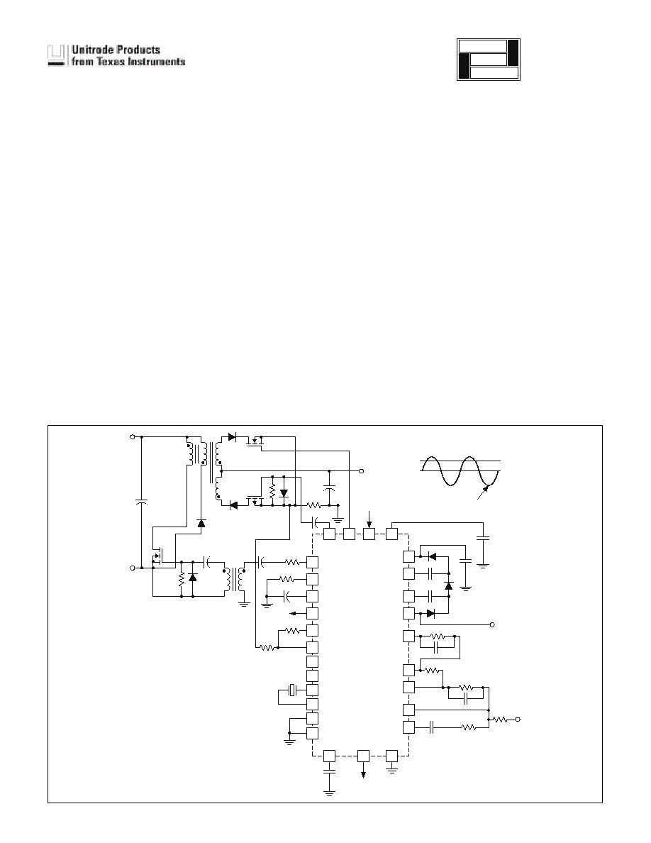
Source Ringer Controller
15
28
2
4
26
27
25
6
5
7
18
16
17
10
OUT2
NEG2
VS2
VDD
VS1
VCP
OUT1
NEG1
REF
ENBL
GD3
GD2
5V
SINFLT
24
23
1
11
12
OUTDC
NEGDC
RT
RGOOD
CT
GD1
AMPOUT
XTAL1
XTAL2
13
14
22
21
AMPIN
FS0
FS1
20
19
V
IN
48V
UCC3750
9
8
3
SINREF
SWRLY
GND
C17
0.047
µ
F
V
OUT
0V
≠48V
V
OUT
TYPICAL APPLICATION
FEATURES
∑
Provides Control for Flyback Based
Four Quadrant Amplifier Topology
∑
Onboard Sine Wave Reference with
Low THD
∑
Selectable Ringing Frequency for
Different Phone Systems (20Hz,
25Hz and 50Hz)
∑
Programmable Output Amplitude and
DC Offset
∑
DC Current Limiting for Short Circuit
Protection
∑
Secondary Side Voltage Mode
Control
∑
Operates from a Single 5V Supply
SLUS172B - DECEMBER 1999 - REVISED SEPTEMBER 2000
UDG-99073
application
INFO
available
2
UCC2750
UCC3750
ABSOLUTE MAXIMUM RATINGS
Input Supply Voltage
VDD . . . . . . . . . . . . . . . . . . . . . . . . . . . . . . . . . . . . . . . . 7.5V
Maximum Forced Voltage
VCP . . . . . . . . . . . . . . . . . . . . . . . . . . . . . . . . ≠0.3V to 13.2V
VS1, VS2. . . . . . . . . . . . . . . . . . . . . . . . . . . . . . . ≠0.3V to 5V
OUT1, OUT2, AMPOUT, OUTDC
Maximum Forced Voltage . . . . . . . . . . . . . . . . ≠0.3V to 7.5V
Maximum Forced Current . . . . . . . . . . . . . . Internally Limited
NEG1, NEG2, AMPIN, NEGDC
Maximum Forced Voltage . . . . . . . . . . . . . . . . ≠0.3V to 7.5V
SINREF, SINFLT
Maximum Forced Voltage . . . . . . . . . . . . . . . . ≠0.3V to 7.5V
Logic Inputs
Maximum Forced Voltage . . . . . . . . . . . . . . . . ≠0.3V to 7.5V
Reference Output Current (REF) . . . . . . . . . . Internally Limited
Output Current (GD1, GD2, GD3)
Pulsed. . . . . . . . . . . . . . . . . . . . . . . . . . . . . . . . . . . . . . . 1.5A
Storage Temperature . . . . . . . . . . . . . . . . . . . ≠65∞C to +150∞C
Junction Temperature . . . . . . . . . . . . . . . . . . . ≠55∞C to +150∞C
Lead Temperature (Soldering, 10 Sec.). . . . . . . . . . . . . +300∞C
Unless otherwise indicated, voltages are reference to ground
and currents are positive into, negative out of the specified ter-
minal. Pulsed is defined as a less than 10% duty cycle with a
maximum duration of 500ns. Consult Packaging Section of
Databook for thermal limitations and considerations of pack-
ages.
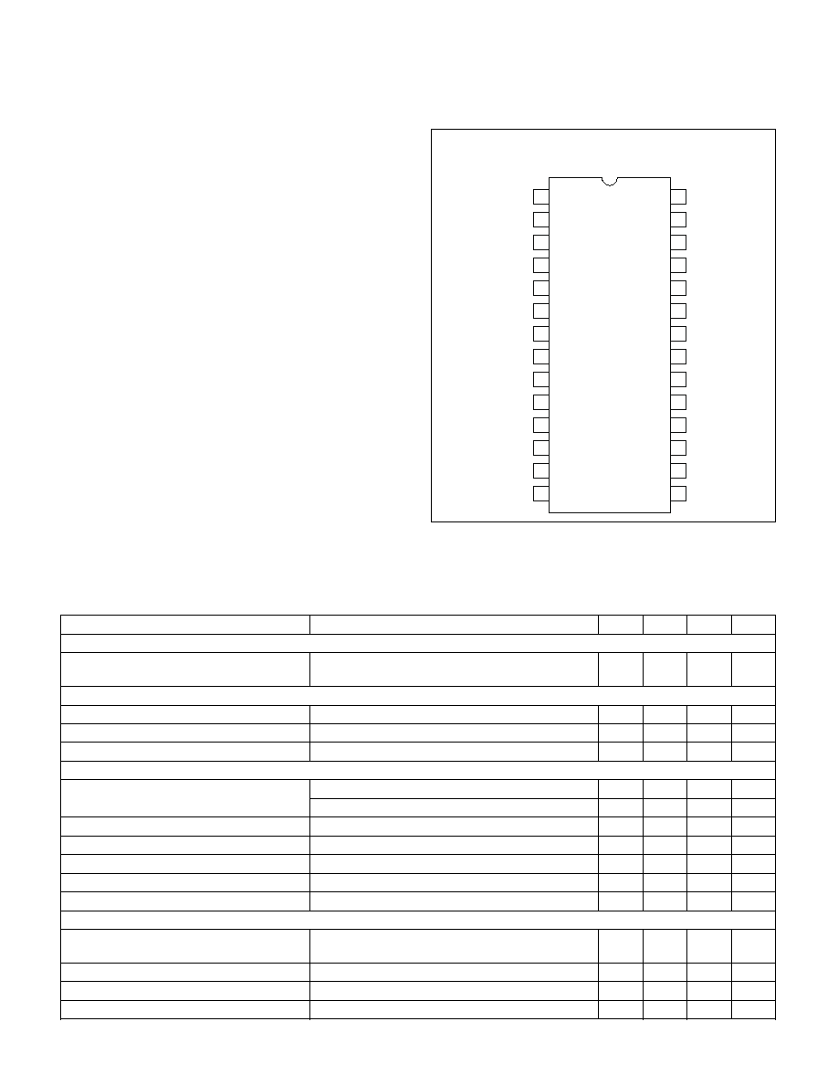
OUTDC
REF
GD3
ENBL
FS 1
RT
CT
XTAL1
GD2
GND
GD1
S INFLT
VDD
S INREF
VCP
VS 1
VS 2
RGOOD
S WRLY
NEGDC
NEG1
XTAL2
FS 0
NEG2
AMP OUT
AMP IN
OUT2
OUT1
14
13
12
11
10
9
8
7
6
5
4
3
2
1
15
16
17
18
19
20
21
22
23
24
25
26
27
28
CONNECTION DIAGRAM
DIL-28, SOIC- 28 (Top View)
N Package, DW Package
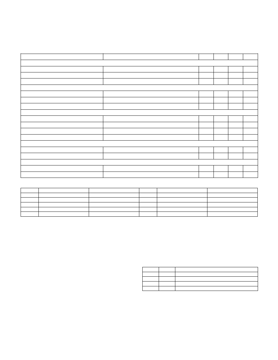
ELECTRICAL CHARACTERISTICS:
Unless otherwise stated, these specifications apply for T
A
= 0∞C to 70∞C for the
UCC3750, ≠40∞C to +85∞C for the UCC2750, RT = 14k, CT = 470pF, C
REF
= 0.1
µ
F, FS0 = 0, FS1 = 0, VDD = 5V. T
A
= T
J
.
PARAMETER
TEST CONDITIONS
MIN
TYP
MAX
UNITS
VDD Supply
Supply Current - Active
With 12V Supplied to V
CP
and Charge Pump
Disabled
0.5
1
mA
Internal Reference w/External Bypass
Output Voltage (REF)
7.3
7.55
7.8
V
Load Regulation
I
REF
= 0mA ≠ 2mA
30
60
mV
Line Regulation
VCP = 10V to 13V, I
REF
= 1mA
3
15
mV
Amplifier
Input Voltage
Error, DC Offset and Amp Amplifiers
2.9
3
3.1
V
DC Limit Amplifier
0.7125
0.75
0.7875
V
Input Bias Current
500
600
nA
AVOL
V
OUT
= 2V to 4V
70
dB
VOH
Source 100
µ
A
5.35
6
7.0
V
VOL
Sink 100
µ
A
0.2
0.65
V
Short Circuit Current
V
IN
= 0V and 5V with V
OUT
= 0V and 5V
0.5
2
3
mA
Sine Reference
Accuracy
T
J
= 25∞C, Program Frequency≠Reference
Frequency
≠1
0
1
Hz
Total Harmonic Distortion
(Note 1)
2
%
Amplitude
Peak
0.475
0.5
0.525
V
Offset
2.85
3.0
3.15
V
3
UCC2750
UCC3750
ELECTRICAL CHARACTERISTICS:
Unless otherwise stated, these specifications apply for T
A
= 0∞C to 70∞C for the
UCC3750, ≠40∞C to +85∞C for the UCC2750, RT = 14k, CT = 470pF, C
REF
= 0.1
µ
F, FS0 = 0, FS1 = 0, VDD = 5V. T
A
= T
J
.
PARAMETER
TEST CONDITIONS
MIN
TYP
MAX
UNITS
Oscillator
Accuracy
108
128
148
kHz
Peak Voltage
4.6
4.75
4.9
V
Valley Voltage
2.9
3.05
3.2
V
Charge Pump
Switch Pull Up Resistance (VS1, VS2)
10
30
Switch Pull Down Resistance (VS1, VS2)
10
30
Output Voltage (VCP)
VDD = 5V, I
VCP
= 10mA
11
12
14
V
Output Drivers
Pull Up Resistance
9
15
Pull Down Resistance
9
15
Rise Time
CL = 2.7nF
50
100
ns
Fall Time
CL = 2.7nF
50
100
ns
Current Limit
DC Limit Threshold Voltage Positive
R5/R6 = 3
0.4
0.5
0.6
V
DC Limit Threshold Voltage Negative
R5/R6 = 3
≠0.6
≠0.5
≠0.4
V
Duty Cycle
Maximum PWM Duty Cycle
48
50
%
Rectifier Duty Cycle
50
%
Note 1: Guaranteed by measuring the steps of the PWL Sine Wave.
STATE
% VCC
VALUE FOR REF = 7.5
STATE
% VCC
VALUE FOR REF = 7.5
0
0.3333
2.5
5
0.4255
3.191
1
0.3384
2.538
6
0.4471
3.353
2
0.3528
2.646
7
0.4616
3.462
3
0.3745
2.808
8
0.4666
3.5
4
0.4
3
AMPIN: Inverting input of the uncommitted amplifier.
AMPOUT: Output of the uncommitted amplifier.
CT: This pin programs the internal PWM oscillator
frequency. Capacitor from CT to GND sets the charge
and discharge time of the oscillator.
ENBL: Logic input which enables the outputs and the
charge pump when high. ENBL should be pulled low to
turn the outputs off.
FS0, FS1: Frequency select pins for the internal
sine-wave generator. Table 1 provides the SINREF
frequencies as a function of FS0 and FS1 when a 32kHz
crystal is used at the crystal inputs (XTAL1, XTAL2).
Other proportional frequencies can be obtained with a
different crystal. Inputs FS0 and FS1 are TTL compatible.
Table I. Frequency selection table
(for 32kHz crystal).
FS0
FS1
SINREF (Hz)
0
0
20
1
0
25
0
1
50
1
1
High Impedance
GD1: Output driver that controls the primary side switch
in a flyback converter through a gate drive transformer.
The output signal on this pin is PWM during positive
power transfer modes and zero during negative power
transfer modes.
PIN DESCRIPTIONS

4
UCC2750
UCC3750
GD2: Output driver that controls the p-channel secondary
side switch in the flyback converter. The output signal on
this pin is PWM during mode 4 (Fig. 2) when the
reference signal is negative and power is being returned
to the input. This pin functions as a synchronous rectifier
output during mode 1 with positive reference signal and
positive power transfer. This output is logically inverted to
provide the correct polarity drive signal for a p-channel
switch.
GD3: Output driver that controls the n-channel secondary
side switch in the flyback converter. The output signal on
this pin is PWM during mode 2 (Fig. 2) when the
reference signal is positive and power is being returned
to the input. This pin functions as a synchronous rectifier
output during mode 3 with a negative reference signal
and positive power transfer.
GND: Reference point for the internal reference and all
thresholds. Also provides the signal return path for all
other pins.
NEG1: Inverting input of the buffer amplifier that acts as
a summing junction for the DC (battery) offset voltage
and sinewave reference.
NEG2: Inverting input of the error amplifier where the
ringer output voltage and the reference signal with the
desired
offset
are
applied
with
a
weighted
sum.
Feedback compensation is connected between NEG2
and OUT2.
NEGDC: Inverting input of the amplifier used for DC
current limiting.
OUT1: Output of the buffer amplifier that provides scaling
and filtering for the reference signal before feeding it into
the error amplifier. This output is also used internally to
select the PWM mode for the flyback converter.
OUT2: Output of the error amplifier. Used to connect
compensation components. This output's absolute value
determines the duty cycle of the PWM pulse. The polarity
of this signal also determines the PWM mode.
OUTDC: Output of the DC current limit amplifier. The DC
current limit is activated when this pin is above 4.5V or
below 1.5V.
REF: Internal 7.5V reference. For best results, bypass to
GND with a ceramic capacitor(>0.1
µ
F).
RGOOD: Logic output that indicates that the error
amplifier output is within range (0< D< 0.5). This pin can
source upto 0.5mA of current.
RT: Resistor from RT to GND helps set the oscillator
frequency. RT programs the charge and discharge
currents of CT.
SINFLT: This signal is the buffered version of SINREF.
This signal is summed with the DC offset level with
appropriate scaling.
SINREF: This pin is the output of the sine-wave
reference generator. It has a high output impedance
(
25k
). A 0.01
µ
F capacitor to GND is recommended to
provide smoothing of the sinewave. When FS0 and FS1
are both set high, the sine reference generator is
disabled allowing this pin to accept an external sinewave
input.
SWRLY: Logic output that leads the battery offset
crossings (by typically 5ms) to allow "zero voltage" relay
switching. This pin can typically source 250
µ
A.
XTAL1: Crystal connection for external crystal. This pin
can be also used to clock the internal sine wave
generator when XTAL2 is connected to VDD/2.
XTAL2: Crystal connection for external crystal.
VCP: External connection for charge pump storage
capacitor. A capacitance
2.2mF is recommended for
low charge pump output ripple. The voltage at this pin is
used by the output drivers for gate drive voltages.
Alternatively, a regulated gate drive voltage (>10V) can
be connected at this pin while leaving the charge pump
circuit at nodes VS1, VS2 disconnected.
VDD: External supply input used to bias internal logic
functions. Typically a regulated 5V supply is connected
between this pin and GND. It also is the input voltage for
the voltage tripler circuit to generate the gate drive
voltage.
VS1, VS2: Voltage switches for the voltage tripler
(charge pump circuit). They provide different voltage
levels to external capacitors in order to pump up the
voltage from VDD to VCP.
PIN DESCRIPTIONS (cont.)
5
UCC2750
UCC3750
The UCC3750 provides complete control and protection
functions for a four quadrant flyback converter used to
generate ring signals for telephone circuits. A typical ap-
plication circuit for a 15 REN ring generator is shown in
Fig. 1.
As shown, the flyback converter takes a DC input (typi-
cally 48V) and provides an isolated output with a pro-
grammable
frequency
(and
amplitude)
AC
signal
superimposed on a programmable DC offset. The power
path consists of a primary side PWM switch Q1, primary
return rectifier DR1, a 4-winding transformer T1, output
rectifiers DR2 and DR3, synchronous/PWM switches Q2
and Q3, and output filter CF. Resistor R
SENSE
provides
the output current sensing for protection circuits.
Different operating modes of the converter are depicted
in Table 2. Fig. 2 shows the output voltage and current
waveforms for a purely capacitive load and identifies the
four operating modes. Fig. 3 shows the PWM waveforms
for the circuit and Fig. 4a - 4d show the equivalent cir-
cuits under the operating modes. The addition of Q2, Q3
and primary diode facilitates true four quadrant operation
where both the output voltage and power transfer can be
bi-directional. Mode 1 is similar to the commonly used
DC-DC converter operation where Q1 is modulated with
the PWM signal and rectification is provided through the
Q2, DR2 path to provide a positive output proportional to
the
increasing,
positive
reference
voltage.
The
pulse-width is controlled by the error amplifier output to
increase or decrease the output as dictated by the refer-
ence. The maximum duty cycle is limited to 50% to pre-
vent DR1 from turning on prior to Q2/DR2.
In mode 2, the reference begins to decrease, necessitat-
ing that the power transfer back to the input. For this
mode, switch Q3 needs to be modulated while DR1 acts
as the rectifier back to the input. The UCC3750 has
mode decoding circuitry which automatically directs the
PWM signal to Q3 and turns off Q1.
APPLICATION INFORMATION
18
21
22
15
FULLWAVE
RECTIFIER
MAG
SIGN
OUT2
MODE SIGN OUT1 OUT2
OUT3
0
0
PWM
OFF
RECIRC
0
1
PWM
OFF
OFF
OFF
PWM
OFF
1
1
0
1
PWM RECIRC
OFF
CONTROL LOGIC
+
≠
REF
ERROR
AMP
V
CM
NEG2
17
16
OUT1
+
≠
REF
DC OFFSET AMP
V
CM
NEG1
2
28
26
V
CP
V
CP
V
CP
GD1
GD2
GD3
+
≠
MODE
SIGN
PWM
+
≠
DC
CURRENT
LIMIT
SINE REFERENCE
GENERATOR
REF
10
SINFLT
9
SINREF
20
FS0
8
SWRLY
19
FS1
XTAL
OSC
14
13
12
11
5
4
7
6
CHARGE
PUMP
INTERNAL
REFERENCE
REF=7.5V
V
CM
= 3.0V
25
V
CM
3
GND
REF
VDD
VS2
VS1
NEGDC
VCP
OUTDC
+
≠
V
CM
4
REF
AMPIN
AMPOUT
XTAL2
XTAL1
MAG
RAMP
CLOCK
GENERATOR
24
RT
23
CT
1
RGOOD
27
ENBL
+
≠
V
CM
AMP
V
CM
DETAILED BLOCK DIAGRAM
UDG-99074
Note: All pin numbers are for N or DW Packages.
Mode
Reference
Polarity
Power
Flow
E.A.
Output
Source
(PWM)
Switch
Rectifier
Switch
1
+
+
≠
Q1
Q2
2
+
≠
+
Q3
(D1)
3
≠
+
+
Q1
Q3
4
≠
≠
≠
Q2
(D1)
Table II. Operating modes.