Document Outline
- Application Notes
- Design Notes

UCC2813-0/-1/-2/-3/-4/-5
UCC3813-0/-1/-2/-3/-4/-5
04/99
FEATURES
100
µ
A Typical Starting Supply Current
500
µ
A Typical Operating Supply Current
Operation to 1MHz
Internal Soft Start
Internal Fault Soft Start
Internal Leading-Edge Blanking of the
Current Sense Signal
1 Amp Totem-Pole Output
70ns Typical Response from
Current-Sense to Gate Drive Output
1.5% Tolerance Voltage Reference
Same Pinout as UCC3802, UC3842, and
UC3842A
DESCRIPTION
The UCC3813-0/-1/-2/-3/-4/-5 family of high-speed, low-power inte-
grated circuits contain all of the control and drive components required
for off-line and DC-to-DC fixed frequency current-mode switching power
supplies with minimal parts count.
These devices have the same pin configuration as the UC3842/3/4/5
family, and also offer the added features of internal full-cycle soft start
and internal leading-edge blanking of the current-sense input.
The UCC3813-0/-1/-2/-3/-4/-5 family offers a variety of package options,
temperature range options, choice of maximum duty cycle, and choice
of critical voltage levels. Lower reference parts such as the UCC3813-3
and UCC3813-5 fit best into battery operated systems, while the higher
reference and the higher UVLO hysteresis of the UCC3813-2 and
UCC3813-4 make these ideal choices for use in off-line power supplies.
The UCC2813-x series is specified for operation from ≠40∞C to +85∞C
and the UCC3813-x series is specified for operation from 0∞C to +70∞C.
BLOCK DIAGRAM
Low Power Economy BiCMOS Current Mode PWM
UDG-96134
Part Number
Maximum Duty Cycle
Reference Voltage
Turn-On Threshold
Turn-Off Threshold
UCCx813-0
100%
5V
7.2V
6.9V
UCCx813-1
50%
5V
9.4V
7.4V
UCCx813-2
100%
5V
12.5V
8.3V
UCCx813-3
100%
4V
4.1V
3.6V
UCCx813-4
50%
5V
12.5V
8.3V
UCCx813-5
50%
4V
4.1V
3.6V
ORDERING INFORMATION
2
UCC2813-0/-1/-2/-3/-4/-5
UCC3813-0/-1/-2/-3/-4/-5
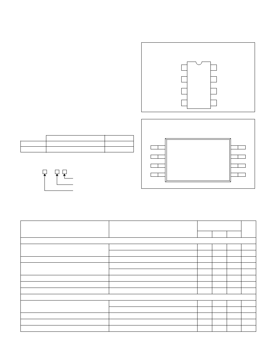
DIL-8 or SOIC-8 (TOP VIEW)
N or D PACKAGE
OUT
VCC
REF
GND
FB
COMP
CS
RC
1
2
3
4
8
7
6
5
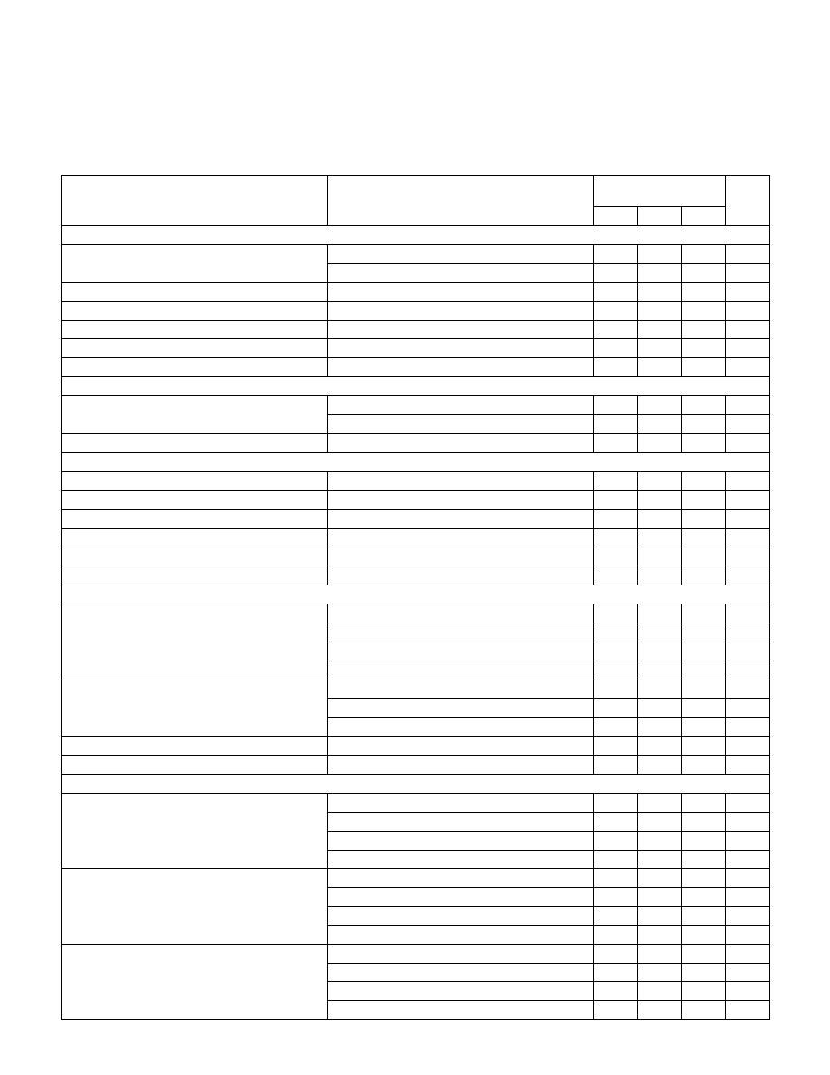
CONNECTION DIAGRAMS
VCC Voltage (Note 2) . . . . . . . . . . . . . . . . . . . . . . . . . . . 12.0V
VCC Current . . . . . . . . . . . . . . . . . . . . . . . . . . . . . . . . . 30.0mA
OUT Current . . . . . . . . . . . . . . . . . . . . . . . . . . . . . . . . . .
1.0A
OUT Energy (Capacitive Load) . . . . . . . . . . . . . . . . . . . 20.0
µ
J
Analog Inputs (FB, CS) . . . . . . . . . . . . . . . . . . . . ≠0.3V to 6.3V
Power Dissipation at T
A
< +25∞C (N Package). . . . . . . . . 1.0W
Power Dissipation at T
A
< +25∞C (D Package). . . . . . . . 0.65W
Storage Temperature . . . . . . . . . . . . . . . . . . . ≠65 C to +150∞C
Junction Temperature . . . . . . . . . . . . . . . . . . . ≠55 C to +150∞C
Lead Temperature (Soldering, 10 Seconds). . . . . . . . . +300∞C
ABSOLUTE MAXIMUM RATINGS (Note 1)
Note 1: All voltages are with respect to GND. All currents are
positive into the specified terminal. Consult Unitrode Integrated
Circuits databook for information regarding thermal specifica-
tions and limitations of packages.
Note 2: In normal operation VCC is powered through a current
limiting resistor. Absolute maximum of 12V applies when VCC
is driven from a low impedance source such that ICC does not
exceed 30mA.
COMP
FB
CS
RC
REF
VCC
OUT
GND
8
7
6
5
1
2
3
4
TSSOP-8 (TOP VIEW)
PW PACKAGE
UCC
PACKAGE
813
TEMPERATURE RANGE
≠
PRODUCT OPTION
ORDERING INFORMATION
TEMPERATURE RANGE
PACKAGES
UCC2813
≠40∞C TO +85∞C
N, D, PW
UCC3813
0∞C TO +70∞C
N, D, PW
ELECTRICAL CHARACTERISTICS
Unless otherwise stated, these specifications apply for ≠40∞C
T
A
+85∞C for
UCC2813-x; 0∞C
T
A
+70∞C for UCC3813-x; VCC = 10V (Note 3); RT = 100k from REF to RC; CT=330pF from RC to GND;
0.1
µ
F capacitor from VCC to GND; 0.1
µ
F capacitor from VREF to GND. T
A
= T
J
.
PARAMETER
TEST CONDITIONS
UCC2813-x
UCC3813-x
UNITS
MIN
TYP
MAX
Reference Section
Output Voltage
T
J
= +25∞C, I = 0.2mA, UCCx813-0/-1/-2/-4
4.925
5.00
5.075
V
T
J
= +25∞C, I = 0.2mA, UCCx813-5
3.94
4.00
4.06
V
Load Regulation
0.2mA < I < 5mA
10
30
mV
Total Variation
UCCx813 -0-1/-2/-4 (Note 7)
4.84
5.00
5.10
V
UCCx813-5 (Note 7)
3.84
4.00
4.08
V
Output Noise Voltage
10Hz
f
10kHz, T
J
= +25∞C (Note 9)
70
µ
V
Long Term Stability
T
A
= +125 C, 1000 Hours (Note 9)
5
mV
Output Short Circuit
≠5
≠35
mA
Oscillator Section
Oscillator Frequency
UCCx813-0/-1/-2/-4 (Note 4)
40
46
52
kHz
UCCx813-5 (Note 4)
26
31
36
kHz
Temperature Stability
(Note 9)
2.5
%
Amplitude Peak-to-Peak
2.25
2.40
2.55
V
Oscillator Peak Voltage
2.45
V
3
UCC2813-0/-1/-2/-3/-4/-5
UCC3813-0/-1/-2/-3/-4/-5
ELECTRICAL CHARACTERISTICS
Unless otherwise stated, these specifications apply for ≠40∞C
T
A
+85∞C for
UCC2813-x; 0∞C
T
A
+70∞C for UCC3813-x; VCC = 10V (Note 3); RT = 100k from REF to RC; CT=330pF from RC to GND;
0.1
µ
F capacitor from VCC to GND; 0.1
µ
F capacitor from VREF to GND. T
A
= T
J
.
PARAMETER
TEST CONDITIONS
UCC2813-x
UCC3813-x
UNITS
MIN
TYP
MAX
Error Amplifier Section
Input Voltage
COMP = 2.5V; UCCx813-0/-1/-2/-4
2.42
2.50
2.56
V
COMP = 2.0V; UCCx813-3/-5
1.92
2.0
2.05
V
Input Bias Current
≠
2
2
µ
A
Open Loop Voltage Gain
60
80
dB
COMP Sink Current
FB = 2.7V, COMP = 1.1V
0.4
2.5
mA
COMP Source Current
FB = 1.8V, COMP = REF ≠ 1.2V
≠0.2
≠0.5
≠0.8
mA
Gain Bandwidth Product
(Note 9)
2
MHz
PWM Section
Maximum Duty Cycle
UCCx813-0/-2/-3
97
99
100
%
UCCx813-1/-4/-5
48
49
50
Minimum Duty Cycle
COMP = 0V
0
%
Current Sense Section
Gain
(Note 5)
1.10
1.65
1.80
V/V
Maximum Input Signal
COMP = 5V (Note 6)
0.9
1.0
1.1
V
Input Bias Current
≠
200
200
nA
CS Blank Time
50
100
150
ns
Over-Current Threshold
1.32
1.55
1.70
V
COMP to CS Offset
CS = 0V
0.45
0.90
1.35
V
Output Section
OUT Low Level
I = 20mA, all parts
0.1
0.4
V
I = 200mA, all parts
0.35
0.90
V
I = 50mA, VCC = 5V, UCCx813-3/-5
0.15
0.40
V
I = 20mA, VCC = 0V, all parts
0.7
1.2
V
OUT High V
SAT
(V
CC
-OUT)
I = ≠20mA, all parts
0.15
0.40
V
I = ≠200mA, all parts
1.0
1.9
V
I = ≠50mA,VCC = 5V, UCCx813-3/-5
0.4
0.9
V
Rise Time
C
L
= 1nF
41
70
ns
Fall Time
C
L
= 1nF
44
75
ns
Undervoltage Lockout Section
Start Threshold (Note 8)
UCCx813-0
6.6
7.2
7.8
V
UCCx813-1
8.6
9.4
10.2
V
UCCx813-2/-4
11.5
12.5
13.5
V
UCCx813-3/-5
3.7
4.1
4.5
V
Stop Threshold (Note 8)
UCC1813-0
6.3
6.9
7.5
V
UCC1813-1
6.8
7.4
8.0
V
UCCx813-2/-4
7.6
8.3
9.0
V
UCCx813-3/-5
3.2
3.6
4.0
V
Start to Stop Hysteresis
UCCx813-0
0.12
0.3
0.48
V
UCCx813-1
1.6
2
2.4
V
UCCx813-2/-4
3.5
4.2
5.1
V
UCCx813-3/-5
0.2
0.5
0.8
V
4
UCC2813-0/-1/-2/-3/-4/-5
UCC3813-0/-1/-2/-3/-4/-5
ELECTRICAL CHARACTERISTICS
Unless otherwise stated, these specifications apply for ≠40∞C
T
A
+85∞C for
UCC2813-x; 0∞C
T
A
+70∞C for UCC3813-x; VCC = 10V (Note 3); RT = 100k from REF to RC; CT=330pF from RC to GND;
0.1
µ
F capacitor from VCC to GND; 0.1
µ
F capacitor from VREF to GND. T
A
= T
J
.
PARAMETER
TEST CONDITIONS
UCC2813-x
UCC3813-x
UNITS
MIN
TYP
MAX
Soft Start Section
COMP Rise Time
FB = 1.8V, Rise from 0.5V to REF≠1V
4
ms
Overall Section
Start-up Current
VCC < Start Threshold
0.1
0.23
mA
Operating Supply Current
FB = 0V, CS = 0V, RC = 0V
0.5
1.2
mA
VCC Internal Zener Voltage
ICC = 10mA (Note 8)
12
13.5
15
V
VCC Internal Zener Voltage Minus Start
Threshold Voltage
UCCx813-2/-4
0.5
1.0
V
Note 3: Adjust VCC above the start threshold before setting at 10V.
Note 4: Oscillator frequency for the UCCx813-0, UCCx813-2 and UCCx813-3 is the output frequency.
Oscillator frequency for the UCCx813-1, UCCx813-4 and UCCx813-5 is twice the output frequency.
Note 5: Gain is defined by:
A
V
V
V
V
COMP
CS
CS
0
0 8
.
.
Note 6: Parameter measured at trip point of latch with Pin 2 at 0V.
Note 7: Total Variation includes temperature stability and load regulation.
Note 8: Start Threshold, Stop Threshold and Zener Shunt Thresholds track one another.
Note 9: Guaranteed by design. Not 100% tested in production.
COMP: COMP is the output of the error amplifier and the
input of the PWM comparator.
Unlike other devices, the error amplifier in the UCC3813
family is a true, low output-impedance, 2MHz operational
amplifier. As such, the COMP terminal can both source
and sink current. However, the error amplifier is internally
current limited, so that you can command zero duty cycle
by externally forcing COMP to GND.
The UCC3813 family features built-in full cycle Soft Start.
Soft Start is implemented as a clamp on the maximum
COMP voltage.
FB: FB is the inverting input of the error amplifier. For
best stability, keep FB lead length as short as possible
and FB stray capacitance as small as possible.
CS: CS is the input to the current sense comparators.
The UCC3813 family has two different current sense
comparators: the PWM comparator and an over-current
comparator.
The UCC3813 family contains digital current sense filter-
ing, which disconnects the CS terminal from the current
sense comparator during the 100ns interval immediately
following the rising edge of the OUT pin. This digital filter-
ing, also called leading-edge blanking, means that in
most applications, no analog filtering (RC filter) is re-
quired on CS. Compared to an external RC filter tech-
nique, the leading-edge blanking provides a smaller
effective CS to OUT propagation delay. Note, however,
that the minimum non-zero On-Time of the OUT signal is
directly affected by the leading-edge-blanking and the
CS to OUT propagation delay.
The over-current comparator is only intended for fault
sensing, and exceeding the over-current threshold will
cause a soft start cycle.
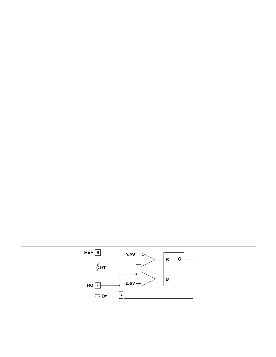
RC: RC is the oscillator timing pin. For fixed frequency
operation, set timing capacitor charging current by con-
necting a resistor from REF to RC. Set frequency by con-
necting a timing capacitor from RC to GND. For best
performance, keep the timing capacitor lead to GND as
short and direct as possible. If possible, use separate
ground traces for the timing capacitor and all other func-
tions.
PIN DESCRIPTIONS
5
UCC2813-0/-1/-2/-3/-4/-5
UCC3813-0/-1/-2/-3/-4/-5
The frequency of oscillation can be estimated with the
following equations:
UCCx813-0/-1/-2/-4:
F
R C
=
∑
1 5
.
UCCx813-3, UCCx813-5:
F
R C
=
∑
1 0
.
where frequency is in Hz, resistance is in
, and capaci-
tance is in farads. The recommended range of timing re-
sistors is between 10k and 200k and timing capacitor is
100pF to 1000pF. Never use a timing resistor less than
10k.
GND: GND is reference ground and power ground for all
functions on this part.
OUT: OUT is the output of a high-current power driver
capable of driving the gate of a power MOSFET with
peak currents exceeding
±
750mA. OUT is actively held
low when VCC is below the UVLO threshold.
The high-current power driver consists of FET output de-
vices, which can switch all of the way to GND and all of
the way to VCC. The output stage also provides a very
low impedance to overshoot and undershoot. This means
that in many cases, external schottky clamp diodes are
not required.
VCC: VCC is the power input connection for this device.
In normal operation VCC is powered through a current
limiting resistor. Although quiescent VCC current is very
low, total supply current will be higher, depending on
OUT current. Total VCC current is the sum of quiescent
VCC current and the average OUT current. Knowing the
operating frequency and the MOSFET gate charge (Qg),
average OUT current can be calculated from:
I
Q
F
OUT
g
=
∑
.
To prevent noise problems, bypass VCC to GND with a
ceramic capacitor as close to the VCC pin as possible.
An electrolytic capacitor may also be used in addition to
the ceramic capacitor.
REF: REF is the voltage reference for the error amplifier
and also for many other functions on the IC. REF is also
used as the logic power supply for high speed switching
logic on the IC.
When VCC is greater than 1V and less than the UVLO
threshold, REF is pulled to ground through a 5k
resis-
tor. This means that REF can be used as a logic output
indicating power system status. It is important for refer-
ence stability that REF is bypassed to GND with a ce-
ramic capacitor as close to the pin as possible. An
electrolytic capacitor may also be used in addition to the
ceramic capacitor. A minimum of 0.1
µ
F ceramic is re-
quired. Additional REF bypassing is required for external
loads greater than 2.5mA on the reference.
To prevent noise problems with high speed switching
transients, bypass REF to ground with a ceramic capaci-
tor very close to the IC package.
PIN DESCRIPTIONS (cont.)
Figure 1. Oscillator.
APPLICATION INFORMATION
The UCC3813-0/-1/-2/-3/-4/-5 oscillator generates a sawtooth waveform on RC. The rise time is set by the time constant of R
T
and C
T
. The fall time is set by CT and an internal transistor on-resistance of approximately 125
. During the fall time, the output
is off and the maximum duty cycle is reduced below 50% or 100% depending on the part number. Larger timing capacitors in-
crease the discharge time and reduce the maximum duty cycle and frequency.
UDG-96139