Document Outline
- FEATURES
- DESCRIPTION
- BLOCK DIAGRAM
- PIN CONNECTION DIAGRAM
- ABSOLUTE MAXIMUM RATINGS
- ELECTRICAL CHARACTERISTICS
- PIN ASSIGNMENTS
- Pin Descriptions
- CAI:
- CAOUT:
- CT:
- DRVOUT:
- GND:
- IAC:
- MOUT:
- OVP/EN:
- PKLMT:
- RT:
- SS:
- VAOUT:
- VCC:
- VFF:
- VSENSE:
- VREF:
- APPLICATION INFORMATION
- Power Stage
- Power switch selection:
- Softstart
- Multiplier
- Voltage Loop
- Current Loop
- Start Up
- Capacitor Ripple Reduction
- References and Resources:
- Related Products
- MECHANICAL DATA
- D (R-PDSO-G**) PLASTIC SMALL-OUTLINE PACKAGE
- N (R-PDIP-T**) PLASTIC DUAL-IN-LINE PACKAGE
- PW (R-PDSO-G**) PLASTIC SMALL-OUTLINE PACKAGE
UCC2817A, UCC2818A
UCC3817A, UCC3818A
SLUS577A - SEPTEMBER, 2003 - REVISED OCTOBER 2003
BiCMOS POWER FACTOR PREREGULATOR
1
www.ti.com
FEATURES
D
Controls Boost Preregulator to Near-Unity
Power Factor
D
Limits Line Distortion
D
World Wide Line Operation
D
Over-Voltage Protection
D
Accurate Power Limiting
D
Average Current Mode Control
D
Improved Noise Immunity
D
Improved Feed-Forward Line Regulation
D
Leading Edge Modulation
D
150-
�
A Typical Start-Up Current
D
Low-Power BiCMOS Operation
D
12-V to 17-V Operation
DESCRIPTION
The UCC3817A and the UCC3818A family
provides all the functions necessary for active
power factor corrected preregulators. The
controller achieves near unity power factor by
shaping the ac input line current waveform to
correspond to that of the ac input line voltage.
Average current mode control maintains stable,
low distortion sinusoidal line current.
Designed in Texas Instrument's BiCMOS process,
the UCC3817A/UCC3818A offers new features
such as lower start-up current, lower power
dissipation, overvoltage protection, a shunt UVLO
detect circuitry, a leading-edge modulation
technique to reduce ripple current in the bulk
capacitor and an improved, low-offset (
�
2 mV)
current amplifier to reduce distortion at light load
conditions.
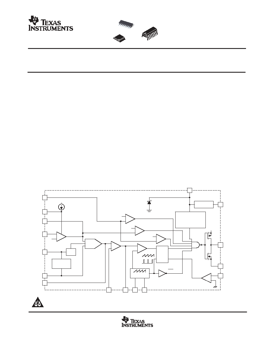
BLOCK DIAGRAM
UDG-03122
VREF
9
2
16
1
15
10
5
4
DRVOUT
GND
CAI
VCC
OVP/EN
VAOUT
1.9 V
PKLMT
7.5 V
REFERENCE
UVLO
16 V/10 V (UCC3817A)
10.5 V/10 V (UCC3818A)
VCC
3
OSCILLATOR
12
RT
14
CT
S
Q
R
PWM
LATCH
+
-
PWM
CAOUT
+
-
+
-
+
-
SS
VOLTAGE
ERROR AMP
8.0 V
13
7
11
VSENSE
VFF
8
IAC
6
MOUT
MIRROR
2:1
X2
+
-
7.5 V
ENABLE
OVP
�
X
X
MULT
OSC
CLK
CLK
CURRENT
AMP
16 V (FOR UCC3817A ONLY)
+
-
0.33 V
ZERO POWER
R
+
-
PRODUCTION DATA information is current as of publication date.
Products conform to specifications per the terms of Texas Instruments
standard warranty. Production processing does not necessarily include
testing of all parameters.
Copyright
2003, Texas Instruments Incorporated
Please be aware that an important notice concerning availability, standard warranty, and use in critical applications of
Texas Instruments semiconductor products and disclaimers thereto appears at the end of this data sheet.

UCC2817A, UCC2818A
UCC3817A, UCC3818A
SLUS577A - SEPTEMBER, 2003 - REVISED OCTOBER 2003
2
www.ti.com
DESCRIPTION (CONTINUED)
The UCC3817A/18A family of PFC Controllers is directly pin for pin compatible with the UCC3817/18 family of
devices. Only the output stage of UCC3817A family has been modified to allow use of a smaller external gate
drive resistor values. For some power supply designs where an adequately high enough gate drive resistor can
not be used, the UCC3817A/18A family offers a more robust output stage at the cost of increasing the internal
gate resistances. The gate drive of the UC3817A/18A family however remains strong at
�
1.2 A of peak current
capability.
UCC3817A offers an on-chip shunt regulator with low start-up current, suitable for applications utilizing a
bootstrap supply. UCC3818A is intended for applications with a fixed supply (VCC). Both devices are available
in the 16-pin D, N and PW packages.
PIN CONNECTION DIAGRAM
D, N, AND PW PACKAGES
(TOP VIEW)
1
2
3
4
5
6
7
8
16
15
14
13
12
11
10
9
GND
PKLMT
CAOUT
CAI
MOUT
IAC
VAOUT
VFF
DRVOUT
VCC
CT
SS
RT
VSENSE
OVP/EN
VREF
AVAILABLE OPTIONS TABLE
PACKAGE DEVICES
T = T
SOIC (D) PACKAGE(1)
PDIP (N) PACKAGE
TSSOP (PW) PACKAGE(1)
TA = TJ
Turn-on
Threshold
16 V
Turn-on
Threshold
10.2 V
Turn-on
Threshold
16 V
Turn-on
Threshold
10.2 V
Turn-on
Threshold
16 V
Turn-on
Threshold
10.2 V
-40
�
C to 85
�
C
UCC2817AD
UCC2818AD
UCC2817AN
UCC2818AN
UCC2817APW
UCC2818APW
0
�
C to 70
�
C
UCC3817AD
UCC3818AD
UCC3817AN
UCC3818AN
UCC3817APW
UCC3818APW
NOTES: (1) The D and PW packages are available taped and reeled. Add R suffix to the device type (e.g. UCC3817ADR) to order quantities
of 2,500 devices per reel (D package) and 2,000 devices per reel (for PW package). Bulk quantities are 40 units (D package) and
90 units (PW package) per tube.
THERMAL RESISTANCE TABLE
PACKAGE
jc(
�
C/W)
ja(
�
C/W)
SOIC-16 (D)
22
40 to 70
(1)
PDIP-16 (N)
12
25 to 50
(1)
TSSOP-16 (PW)
14
(2)
123 to 147
(2)
NOTES: (1) Specified
ja (junction to ambient) is for devices mounted to 5-inch2 FR4 PC board with one ounce copper
where noted. When resistance range is given, lower values are for 5 inch2 aluminum PC board. Test PWB
was 0.062 inch thick and typically used 0.635-mm trace widths for power packages and 1.3-mm trace
widths for non-power packages with a 100-mil x 100-mil probe land area at the end of each trace.
(2) Modeled data. If value range given for
ja, lower value is for 3x3 inch. 1 oz internal copper ground plane,
higher value is for 1x1-inch. ground plane. All model data assumes only one trace for each non-fused
lead.
UCC2817A, UCC2818A
UCC3817A, UCC3818A
SLUS577A - SEPTEMBER, 2003 - REVISED OCTOBER 2003
3
www.ti.com
ABSOLUTE MAXIMUM RATINGS
over operating free-air temperature (unless otherwise noted)
UCCx81xA
UNIT
Supply voltage VCC
18
V
Supply current ICC
20
mA
Gate drive current, continuous
0.2
A
Gate drive current
1.2
A
Input voltage, CAI, MOUT, SS
8
Input voltage, PKLMT
5
V
Input voltage, VSENSE, OVP/EN
10
V
Input current, RT, IAC, PKLMT
10
mA
Input current, VCC (no switching)
20
mA
Maximum negative voltage, DRVOUT, PKLMT, MOUT
-0.5
V
Power dissipation
1
W
Junction temperature, TJ
-55 to 150
Storage temperature, Tstg
-65 to 150
�
C
Lead temperature, Tsol (soldering, 10 seconds)
300
C
Power dissipation
1
W
Stresses beyond those listed under "absolute maximum ratings" may cause permanent damage to the device. These are stress ratings only, and
functional operation of the device at these or any other conditions beyond those indicated under recommended operating conditions is not implied.
Exposure to absolute-maximum-rated conditions for extended periods may affect device reliability.
ELECTRICAL CHARACTERISTICS
T
A
= 0
�
C to 70
�
C for the UCC3817A and T
A
= -40
�
C to 85
�
C for the UCC2817A, T
A
= T
J,
VCC = 12 V, R
T
= 22 k
,
C
T
= 270 pF, (unless otherwise noted)
PARAMETER
TEST CONDITIONS
MIN
TYP
MAX
UNITS
Supply Current Section
Supply current, off
VCC = (VCC turn-on threshold -0.3 V)
150
300
�
A
Supply current, on
VCC = 12 V, No load on DRVOUT
2
4
6
mA
UVLO Section
VCC turn-on threshold (UCCx817)
15.4
16
16.6
VCC turn-off threshold (UCCx817)
9.4
9.7
UVLO hysteresis (UCCx817)
5.8
6.3
Maximum shunt voltage (UCCx817)
IVCC = 10 mA
15.4
17
17.5
V
VCC turn-on threshold (UCCx818)
9.7
10.2
10.8
V
VCC turn-off threshold (UCCx818)
9.4
9.7
UVLO hysteresis (UCCx818)
0.3
0.5
Voltage Amplifier Section
Input voltage
TA = 0
�
C to 70
�
C
7.387
7.5
7.613
V
Input voltage
TA = -40
�
C to 85
�
C
7.369
7.5
7.631
V
VSENSE bias current
VSENSE = VREF,
VAOUT = 2.5 V
50
200
nA
Open loop gain
VAOUT = 2 V to 5 V
50
90
dB
High-level output voltage
IL = -150
�
A
5.3
5.5
5.6
V
Low-level output voltage
IL = 150
�
A
0
50
150
mV

UCC2817A, UCC2818A
UCC3817A, UCC3818A
SLUS577A - SEPTEMBER, 2003 - REVISED OCTOBER 2003
4
www.ti.com
ELECTRICAL CHARACTERISTICS
T
A
= 0
�
C to 70
�
C for the UCC3817A and T
A
= -40
�
C to 85
�
C for the UCC2817A, T
A
= T
J,
VCC = 12 V, R
T
= 22 k
,
C
T
= 270 pF, (unless otherwise noted)
PARAMETER
TEST CONDITIONS
MIN
TYP
MAX
UNITS
Over Voltage Protection and Enable Section
Over voltage reference
VREF
+0.48
VREF
+0.50
VREF
+0.52
V
Hysteresis
300
500
600
mV
Enable threshold
1.7
1.9
2.1
V
Enable hysteresis
0.1
0.2
0.3
V
Current Amplifier Section
Input offset voltage
VCM = 0 V,
VCAOUT = 3 V
-3.5
0
2.5
mV
Input bias current
VCM = 0 V,
VCAOUT = 3 V
-50
-100
nA
Input offset current
VCM = 0 V,
VCAOUT = 3 V
25
100
nA
Open loop gain
VCM = 0 V,
VCAOUT = 2 V to 5 V
90
dB
Common-mode rejection ratio
VCM = 0 V to 1.5 V,
VCAOUT = 3 V
60
80
dB
High-level output voltage
IL = -120
�
A
5.6
6.5
6.8
V
Low-level output voltage
IL = 1 mA
0.1
0.2
0.5
V
Gain bandwidth product
(1)
2.5
MHz
Voltage Reference Section
Input voltage
TA = 0
�
C to 70
�
C
7.387
7.5
7.613
V
Input voltage
TA = -40
�
C to 85
�
C
7.369
7.5
7.631
V
Load regulation
IREF = 1 mA to 2 mA
0
10
mV
Line regulation
VCC = 10.8 V to 15 V(2)
0
10
mV
Short-circuit current
VREF = 0 V
-20
-25
-50
mA
Oscillator Section
Initial accuracy
TA = 25
�
C
85
100
115
kHz
Voltage stability
VCC = 10.8 V to 15 V
-1
1
%
Total variation
Line, temp
80
120
kHz
Ramp peak voltage
4.5
5
5.5
Ramp amplitude voltage
(peak to peak)
3.5
4
4.5
V
Peak Current Limit Section
PKLMT reference voltage
-15
15
mV
PKLMT propagation delay
150
350
500
ns
NOTES:
1. Ensured by design, not production tested.
2. Reference variation for VCC < 10.8 V is shown in Figure 8.
UCC2817A, UCC2818A
UCC3817A, UCC3818A
SLUS577A - SEPTEMBER, 2003 - REVISED OCTOBER 2003
5
www.ti.com
ELECTRICAL CHARACTERISTICS
T
A
= 0
�
C to 70
�
C for the UCC3817A and T
A
= -40
�
C to 85
�
C for the UCC2817A, T
A
= T
J,
VCC = 12 V, R
T
= 22 k
,
C
T
= 270 pF, (unless otherwise noted)
PARAMETER
TEST CONDITIONS
MIN
TYP
MAX
UNITS
Multiplier Section
IMOUT, high line, low power output
current, (0
�
C to 85
�
C)
IAC = 500
�
A, VFF = 4.7 V,
VAOUT = 1.25 V
0
-6
-20
IMOUT, high line, low power output
current, (-40
�
C to 85
�
C)
IAC = 500
�
A, VFF = 4.7 V,
VAOUT = 1.25 V
0
-6
-23
IMOUT, high line, high power output
current
IAC = 500
�
A, VFF = 4.7 V,
VAOUT = 5 V
-70
-90
-105
�
A
IMOUT, low line, low power output
current
IAC = 150
�
A, VFF = 1.4 V,
VAOUT = 1.25 V
-10
-19
-50
�
A
IMOUT, low line, high power output
current
IAC = 150
�
A, VFF = 1.4 V,
VAOUT = 5 V
-268
-300
-345
IMOUT, IAC limited output current
IAC = 150
�
A, VFF = 1.3 V,
VAOUT = 5 V
-250
-300
-400
Gain constant (K)
IAC = 300
�
A, VFF = 3 V,
VAOUT = 2.5 V
0.5
1
1.5
1/V
IMOUT, zero current
IAC = 150
�
A, VFF = 1.4 V,
VAOUT = 0.25 V
0
-2
IMOUT, zero current
IAC = 500
�
A, VFF = 4.7 V,
VAOUT = 0.25 V
0
-2
A
IMOUT, zero current, (0
�
C to 85
�
C)
IAC = 500
�
A, VFF = 4.7 V,
VAOUT = 0.5 V
0
-3
�
A
IMOUT, zero current, (-40
�
C to 85
�
C)
IAC = 500
�
A, VFF = 4.7 V,
VAOUT = 0.5 V
0
-3.5
Power limit (IMOUT x VFF)
IAC = 150
�
A, VFF = 1.4 V,
VAOUT = 5 V
-375
-420
-485
�
W
Feed-Forward Section
VFF output current
IAC = 300
�
A
-140
-150
-160
�
A
Soft Start Section
SS charge current
-6
-10
-16
�
A
Gate Driver Section
Pullup resistance
IO = �100 mA to -200 mA
9
12
Pulldown resistance
IO = 100 mA
4
10
Output rise time
CL = 1 nF,
RL = 10
,
VDRVOUT = 0.7 V to 9.0 V
25
50
ns
Output fall time
CL = 1 nF,
RL = 10
,
VDRVOUT = 9.0 V to 0.7 V
10
50
ns
Maximum duty cycle
93%
95%
99%
Minimum controlled duty cycle
At 100 kHz
2%
Zero Power Section
Zero power comparator threshold
Measured on VAOUT
0.20
0.33
0.50
V

UCC2817A, UCC2818A
UCC3817A, UCC3818A
SLUS577A - SEPTEMBER, 2003 - REVISED OCTOBER 2003
6
www.ti.com
PIN ASSIGNMENTS
TERMINAL
I/O
DESCRIPTION
NAME
NO.
I/O
DESCRIPTION
CAI
4
I
Current amplifier noninverting input
CAOUT
3
O
Current amplifier output
CT
14
I
Oscillator timing capacitor
DRVOUT
16
O
Gate drive
GND
1
-
Ground
IAC
6
I
Current proportional to input voltage
MOUT
5
I/O
Multiplier output and current amplifier inverting input
OVP/EN
10
I
Over-voltage/enable
PKLMT
2
I
PFC peak current limit
RT
12
I
Oscillator charging current
SS
13
I
Soft-start
VAOUT
7
O
Voltage amplifier output
VCC
15
I
Positive supply voltage
VFF
8
I
Feed-forward voltage
VSENSE
11
I
Voltage amplifier inverting input
VREF
9
O
Voltage reference output
Pin Descriptions
CAI: Place a resistor between this pin and the GND side of current sense resistor. This input and the inverting
input (MOUT) remain functional down to and below GND.
CAOUT: This is the output of a wide bandwidth operational amplifier that senses line current and commands
the PFC pulse-width modulator (PWM) to force the correct duty cycle. Compensation components are placed
between CAOUT and MOUT.
CT: A capacitor from CT to GND sets the PWM oscillator frequency according to:
f
[
0.6
RT
CT
The lead from the oscillator timing capacitor to GND should be as short and direct as possible.
DRVOUT: The output drive for the boost switch is a totem-pole MOSFET gate driver on DRVOUT. To avoid the
excessive overshoot of the DRVOUT while driving a capacitive load, a series gate current-limiting/damping
resistor is recommended to prevent interaction between the gate impedance and the output driver. The value
of the series gate resistor is based on the pulldown resistance (R
pulldown
which is 4
typical), the maximum
VCC voltage (VCC), and the required maximum gate drive current (I
MAX
). Using the equation below, a series
gate resistance of resistance 11
would be required for a maximum VCC voltage of 18 V and for 1.2 A of
maximum sink current. The source current will be limited to approximately 900 mA (based on the R
pullup
of 9-
typical).
R
GATE
+
VCC
*
I
MAX
R
pulldown
I
MAX
GND: All voltages measured with respect to ground. VCC and REF should be bypassed directly to GND with
a 0.1-
�
F or larger ceramic capacitor.

UCC2817A, UCC2818A
UCC3817A, UCC3818A
SLUS577A - SEPTEMBER, 2003 - REVISED OCTOBER 2003
7
www.ti.com
Pin Descriptions (cont.)
IAC: This input to the analog multiplier is a current proportional to instantaneous line voltage. The multiplier
is tailored for very low distortion from this current input (I
IAC
) to multiplier output. The recommended maximum
I
IAC
is 500
�
A.
MOUT: The output of the analog multiplier and the inverting input of the current amplifier are connected together
at MOUT. As the multiplier output is a current, this is a high-impedance input so the amplifier can be configured
as a differential amplifier. This configuration improves noise immunity and allows for the leading-edge
modulation operation. The multiplier output current is limited to 2
I
IAC
. The multiplier output current is given
by the equation:
I
MOUT
+
I
IAC
(V
VAOUT
*
1)
V
VFF
2
K
where K
+
1
V
is the multiplier gain constant.
OVP/EN: A window comparator input that disables the output driver if the boost output voltage is a programmed
level above the nominal or disables both the PFC output driver and resets SS if pulled below 1.9 V (typ).
PKLMT: The threshold for peak limit is 0 V. Use a resistor divider from the negative side of the current sense
resistor to VREF to level shift this signal to a voltage level defined by the value of the sense resistor and the
peak current limit. Peak current limit is reached when PKLMT voltage falls below 0 V.
RT: A resistor from RT to GND is used to program oscillator charging current. A resistor between 10 k
and
100 k
is recommended. Nominal voltage on this pin is 3 V.
SS: V
SS
is discharged for V
VCC
low conditions. When enabled, SS charges an external capacitor with a current
source. This voltage is used as the voltage error signal during start-up, enabling the PWM duty cycle to increase
slowly. In the event of a V
VCC
dropout, the OVP/EN is forced below 1.9 V (typ), SS quickly discharges to disable
the PWM.
Note: In an open-loop test circuit, grounding the SS pin does not ensure 0% duty cycle. Please see the
application section for details.
VAOUT: This is the output of the operational amplifier that regulates output voltage. The voltage amplifier output
is internally limited to approximately 5.5 V to prevent overshoot.
VCC: Connect to a stable source of at least 20 mA between 10 V and 17 V for normal operation. Bypass VCC
directly to GND to absorb supply current spikes required to charge external MOSFET gate capacitances. To
prevent inadequate gate drive signals, the output devices are inhibited unless V
VCC
exceeds the upper
under-voltage lockout voltage threshold and remains above the lower threshold.
VFF: The RMS voltage signal generated at this pin by mirroring 1/2 of the I
IAC
into a single pole external filter.
At low line, the VFF voltage should be 1.4 V.
VSENSE: This is normally connected to a compensation network and to the boost converter output through a
divider network.
VREF: VREF is the output of an accurate 7.5-V voltage reference. This output is capable of delivering 20 mA
to peripheral circuitry and is internally short-circuit current limited. VREF is disabled and remains at 0 V when
V
VCC
is below the UVLO threshold. Bypass VREF to GND with a 0.1-
�
F or larger ceramic capacitor for best
stability. Please refer to Figures 8 and 9 for VREF line and load regulation characteristics.
UCC2817A, UCC2818A
UCC3817A, UCC3818A
SLUS577A - SEPTEMBER, 2003 - REVISED OCTOBER 2003
8
www.ti.com
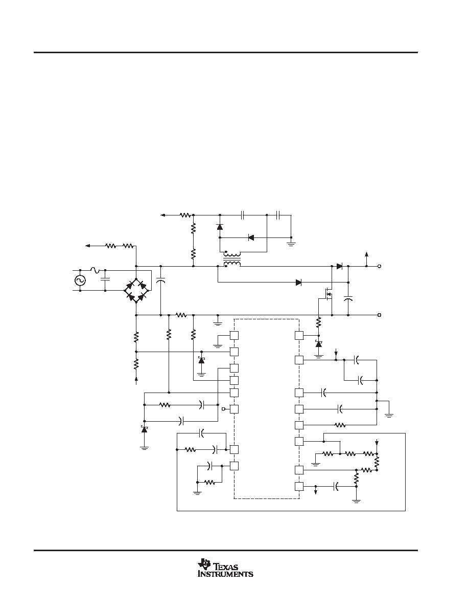
APPLICATION INFORMATION
The UCC3817A is a BiCMOS average current mode boost controller for high power factor, high efficiency
preregulator power supplies. Figure 1 shows the UCC3817A in a 250-W PFC preregulator circuit. Off-line
switching power converters normally have an input current that is not sinusoidal. The input current waveform
has a high harmonic content because current is drawn in pulses at the peaks of the input voltage waveform.
An active power factor correction circuit programs the input current to follow the line voltage, forcing the
converter to look like a resistive load to the line. A resistive load has 0
�
phase displacement between the current
and voltage waveforms. Power factor can be defined in terms of the phase angle between two sinusoidal
waveforms of the same frequency:
PF
+
cos
Q
Therefore, a purely resistive load would have a power factor of 1. In practice, power factors of 0.999 with THD
(total harmonic distortion) of less than 3% are possible with a well-designed circuit. Following guidelines are
provided to design PFC boost converters using the UCC3817A.
UDG-98183
1
11
7
16
GND
DRVOUT
R17
20
15
C3
1
�
F CER
VCC
C2
100
�
F AI EI
14
C1
560pF
13
C4 0.01
�
F
12
R1 12k
R3 20k
R2
499k
R4
249k
R5
10k
C5 1
�
F
9
4
10
VREF
VCC
CT
SS
RT
VSENSE
OVP/EN
VREF
VAOUT
3
8
2
VFF
C6 2.2
�
F
C7 150nF
R7 100k
6
5
R9
4.02k
C8 270pF
R8 12k
D6
R10
4.02k
D5
R11
10k
R12
2k
R14
0.25
3W
C13
0.47
�
F
600V
C14
1.5
�
F
400V
R13
383k
IAC
R18
24k
R15
24k
R16
100
VCC
C10
1
�
F
C11
1
�
F
D7
D8
L1
1mH
D2
6A, 600V
D1
8A, 600V
C12
220
�
F
450V
VOUT
385V-DC
+
-
PKLIMIT
CAOUT
CAI
MOUT
IAC
VO
UCC3817A
VLINE
85-270 VAC
VREF
C9 1.2nF
R6 30k
6A 600V
D3
Q1
F1
VO
D4
R19
499k
R20 274k
R21
383k
AC2
AC1
C15 2.2
�
F
IRFP450
Figure 1. Typical Application Circuit
(1)

UCC2817A, UCC2818A
UCC3817A, UCC3818A
SLUS577A - SEPTEMBER, 2003 - REVISED OCTOBER 2003
9
www.ti.com
APPLICATION INFORMATION
Power Stage
L
BOOST
: The boost inductor value is determined by:
L
BOOST
+
V
IN(min)
D
(
D
I
f
s)
where D is the duty cycle,
I is the inductor ripple current and f
S
is the switching frequency. For the example
circuit a switching frequency of 100 kHz, a ripple current of 875 mA, a maximum duty cycle of 0.688 and a
minimum input voltage of 85 V
RMS
gives us a boost inductor value of about 1 mH. The values used in this
equation are at the peak of low line, where the inductor current and its ripple are at a maximum.
C
OUT
: Two main criteria, the capacitance and the voltage rating, dictate the selection of the output capacitor.
The value of capacitance is determined by the holdup time required for supporting the load after input ac voltage
is removed. Holdup is the amount of time that the output stays in regulation after the input has been removed.
For this circuit, the desired holdup time is approximately 16 ms. Expressing the capacitor value in terms of output
power, output voltage, and holdup time gives the equation:
C
OUT
+
2
P
OUT
D
t
V
OUT
2
*
V
OUT(min)
2
In practice, the calculated minimum capacitor value may be inadequate because output ripple voltage
specifications limit the amount of allowable output capacitor ESR. Attaining a sufficiently low value of ESR often
necessitates the use of a much larger capacitor value than calculated. The amount of output capacitor ESR
allowed can be determined by dividing the maximum specified output ripple voltage by the inductor ripple
current. In this design holdup time was the dominant determining factor and a 220-
�
F, 450-V capacitor was
chosen for the output voltage level of 385 VDC at 250 W.
(2)
(3)

UCC2817A, UCC2818A
UCC3817A, UCC3818A
SLUS577A - SEPTEMBER, 2003 - REVISED OCTOBER 2003
10
www.ti.com
APPLICATION INFORMATION
Power switch selection:
As in any power supply design, tradeoffs between performance, cost and size have
to be made. When selecting a power switch, it can be useful to calculate the total power dissipation in the switch
for several different devices at the switching frequencies being considered for the converter. Total power
dissipation in the switch is the sum of switching loss and conduction loss. Switching losses are the combination
of the gate charge loss, C
OSS
loss and turnon and turnoff losses:
P
GATE
+
Q
GATE
V
GATE
f
S
P
COSS
+
1
2
C
OSS
V
2
OFF
f
S
P
ON
)
P
OFF
+
1
2
V
OFF
I
L
t
ON
)
t
OFF
f
S
where Q
GATE
is the total gate charge, V
GATE
is the gate drive voltage, f
S
is the clock frequency, C
OSS
is the drain
source capacitance of the MOSFET, I
L
is the peak inductor current, t
ON
and t
OFF
are the switching times
(estimated using device parameters R
GATE
, Q
GD
and V
TH
) and V
OFF
is the voltage across the switch during the
off time, in this case V
OFF
= V
OUT
.
Conduction loss is calculated as the product of the R
DS(on)
of the switch (at the worst case junction temperature)
and the square of RMS current:
P
COND
+
R
DS(on)
K
I
2
RMS
where K is the temperature factor found in the manufacturer's R
DS(on)
vs. junction temperature curves.
Calculating these losses and plotting against frequency gives a curve that enables the designer to determine
either which manufacturer's device has the best performance at the desired switching frequency, or which
switching frequency has the least total loss for a particular power switch. For this design example an IRFP450
HEXFET from International Rectifier was chosen because of its low R
DS(on)
and its V
DSS
rating. The IRFP450's
R
DS(on)
of 0.4
and the maximum V
DSS
of 500 V made it an ideal choice. An excellent review of this procedure
can be found in the Unitrode Power Supply Design Seminar SEM1200, Topic 6, Design Review: 140 W, [Multiple
Output High Density DC/DC Converter].
Softstart
The softstart circuitry is used to prevent overshoot of the output voltage during start up. This is accomplished
by bringing up the voltage amplifier's output (V
VAOUT
) slowly which allows for the PWM duty cycle to increase
slowly. Please use the following equation to select a capacitor for the softstart pin.
In this example t
DELAY
is equal to 7.5 ms, which
would yield a C
SS
of 10 nF.
C
SS
+
10
m
A
t
DELAY
7.5 V
In an open-loop test circuit, shorting the softstart pin to ground does not ensure 0% duty cycle. This is due to
the current amplifiers input offset voltage, which could force the current amplifier output high or low depending
on the polarity of the offset voltage. However, in the typical application there is sufficient amount of inrush and
bias current to overcome the current amplifier's offset voltage.
(4)
(5)
(6)
(7)
(8)

UCC2817A, UCC2818A
UCC3817A, UCC3818A
SLUS577A - SEPTEMBER, 2003 - REVISED OCTOBER 2003
11
www.ti.com
APPLICATION INFORMATION
Multiplier
The output of the multiplier of the UCC3817A is a signal representing the desired input line current. It is an input
to the current amplifier, which programs the current loop to control the input current to give high power factor
operation. As such, the proper functioning of the multiplier is key to the success of the design. The inputs to the
multiplier are VAOUT, the voltage amplifier error signal, I
IAC
, a representation of the input rectified ac line
voltage, and an input voltage feedforward signal, V
VFF
. The output of the multiplier, I
MOUT
, can be expressed
as:
I
MOUT
+
I
IAC
V
VAOUT
*
1
K
V
VFF
2
where K is a constant typically equal to 1
V
.
The
electrical characteristics
table covers all the required operating conditions for designing with the
multiplier. Additionally, curves in Figures 10, 11, and 12 provide typical multiplier characteristics over its entire
operating range.
The I
IAC
signal is obtained through a high-value resistor connected between the rectified ac line and the IAC
pin of the UCC3817A/18A. This resistor (R
IAC
) is sized to give the maximum I
IAC
current at high line. For the
UCC3817A/18A the maximum I
IAC
current is about 500
�
A. A higher current than this can drive the multiplier
out of its linear range. A smaller current level is functional, but noise can become an issue, especially at low
input line. Assuming a universal line operation of 85 V
RMS
to 265 V
RMS
gives a R
IAC
value of 750 k
. Because
of voltage rating constraints of standard 1/4-W resistor, use a combination of lower value resistors connected
in series to give the required resistance and distribute the high voltage amongst the resistors. For this design
example two 383-k
resistors were used in series.
The current into the IAC pin is mirrored internally to the VFF pin where it is filtered to produce a voltage feed
forward signal proportional to line voltage. The VFF voltage is used to keep the power stage gain constant; and
to provid input power limiting. Please refer to Texas Instruments application note SLUA196 for detailed
explanation on how the VFF pin provides power limiting. The following equation can be used to size the VFF
resistor (R
VFF
) to provide power limiting where V
IN(min)
is the minimum RMS input voltage and R
IAC
is the total
resistance connected between the IAC pin and the rectified line voltage.
R
VFF
+
1.4 V
V
IN(min)
0.9
2
R
IAC
[
30 k
W
(9)
(10)

UCC2817A, UCC2818A
UCC3817A, UCC3818A
SLUS577A - SEPTEMBER, 2003 - REVISED OCTOBER 2003
12
www.ti.com
APPLICATION INFORMATION
Because the VFF voltage is generated from line voltage it needs to be adequately filtered to reduce total
harmonic distortion caused by the 120 Hz rectified line voltage. Refer to Unitrode Power Supply Design
Seminar, SEM-700 Topic 7, [Optimizing the Design of a High Power Factor Preregulator.] A single pole filter
was adequate for this design. Assuming that an allocation of 1.5% total harmonic distortion from this input is
allowed, and that the second harmonic ripple is 66% of the input ac line voltage, the amount of attenuation
required by this filter is:
1.5 %
66 %
+
0. 022
With a ripple frequency (f
R
) of 120 Hz and an attenuation of 0.022 requires that the pole of the filter (f
P
) be placed
at:
f
P
+
120 Hz
0.022
[
2.6 Hz
The following equation can be used to select the filter capacitor (C
VFF
) required to produce the desired low pass
filter.
C
VFF
+
1
2
p
R
VFF
f
P
[
2.2
m
F
The R
MOUT
resistor is sized to match the maximum current through the sense resistor to the maximum multiplier
current. The maximum multiplier current, or I
MOUT(max)
, can be determined by the equation:
I
MOUT(max)
+
I
IAC
@V
IN(min)
V
VAOUT(max)
*
1 V
K
V
VFF
2
(min)
I
MOUT(max)
for this design is approximately 315
�
A. The R
MOUT
resistor can then be determined by:
R
MOUT
+
V
RSENSE
I
MOUT(max)
In this example V
RSENSE
was selected to give a dynamic operating range of 1.25 V, which gives an R
MOUT
of
roughly 3.91 k
.
(11)
(12)
(13)
(14)
(15)
UCC2817A, UCC2818A
UCC3817A, UCC3818A
SLUS577A - SEPTEMBER, 2003 - REVISED OCTOBER 2003
13
www.ti.com
APPLICATION INFORMATION
Voltage Loop
The second major source of harmonic distortion is the ripple on the output capacitor at the second harmonic
of the line frequency. This ripple is fed back through the error amplifier and appears as a 3rd harmonic ripple
at the input to the multiplier. The voltage loop must be compensated not just for stability but also to attenuate
the contribution of this ripple to the total harmonic distortion of the system. (refer to Figure 2).
RIN
RD
+
-
Rf
Cf
VREF
VOUT
CZ
Figure 2. Voltage Amplifier Configuration
The gain of the voltage amplifier, G
VA
, can be determined by first calculating the amount of ripple present on
the output capacitor. The peak value of the second harmonic voltage is given by the equation:
V
OPK
+
P
IN
2
p
f
R
C
OUT
V
OUT
In this example V
OPK
is equal to 3.91 V. Assuming an allowable contribution of 0.75% (1.5% peak to peak) from
the voltage loop to the total harmonic distortion budget we set the gain equal to:
G
VA
+
D
V
VAOUT
(0.015)
2
V
OPK
where
V
VAOUT
is the effective output voltage range of the error amplifier (5 V for the UCC3817A). The network
needed to realize this filter is comprised of an input resistor, R
IN
, and feedback components C
f
, C
Z
, and R
f
. The
value of R
IN
is already determined because of its function as one half of a resistor divider from V
OUT
feeding
back to the voltage amplifier for output voltage regulation. In this case the value was chosen to be 1 M
. This
high value was chosen to reduce power dissipation in the resistor. In practice, the resistor value would be
realized by the use of two 500-k
resistors in series because of the voltage rating constraints of most standard
1/4-W resistors. The value of C
f
is determined by the equation:
C
f
+
1
2
p
f
R
G
VA
R
IN
(16)
(17)
(18)
UCC2817A, UCC2818A
UCC3817A, UCC3818A
SLUS577A - SEPTEMBER, 2003 - REVISED OCTOBER 2003
14
www.ti.com
APPLICATION INFORMATION
In this example C
f
equals 150 nF. Resistor R
f
sets the dc gain of the error amplifier and thus determines the
frequency of the pole of the error amplifier. The location of the pole can be found by setting the gain of the loop
equation to one and solving for the crossover frequency. The frequency, expressed in terms of input power, can
be calculated by the equation:
f
VI
2
+
P
IN
(2
p
)
2
D
V
VAOUT
V
OUT
R
IN
C
OUT
C
f
f
VI
for this converter is 10 Hz. A derivation of this equation can be found in the Unitrode Power Supply Design
Seminar SEM1000, Topic 1, [A 250-kHz, 500-W Power Factor Correction Circuit Employing Zero Voltage
Transitions].
Solving for R
f
becomes:
R
f
+
1
2
p
f
VI
C
f
or R
f
equals 100 k
.
Due to the low output impedance of the voltage amplifier, capacitor C
Z
was added in series with R
F
to reduce
loading on the voltage divider. To ensure the voltage loop crossed over at f
VI
, C
Z
was selected to add a zero
at a 10th of f
VI
. For this design a 2.2-
�
F capacitor was chosen for C
Z
. The following equation can be used to
calculate C
Z
.
C
Z
+
1
2
p
f
VI
10
R
f
Current Loop
The gain of the power stage is:
G
ID
(s)
+
V
OUT
R
SENSE
s
L
BOOST
V
P
R
SENSE
has been chosen to give the desired differential voltage for the current sense amplifier at the desired
current limit point. In this example, a current limit of 4 A and a reasonable differential voltage to the current amp
of 1 V gives a R
SENSE
value of 0.25
. V
P
in this equation is the voltage swing of the oscillator ramp, 4 V for
the UCC3817A. Setting the crossover frequency of the system to 1/10th of the switching frequency, or 10 kHz,
requires a power stage gain at that frequency of 0.383. In order for the system to have a gain of 1 at the crossover
frequency, the current amplifier needs to have a gain of 1/G
ID
at that frequency. G
EA
, the current amplifier gain
is then:
G
EA
+
1
G
ID
+
1
0.383
+
2.611
(19)
(20)
(21)
(22)
(23)
UCC2817A, UCC2818A
UCC3817A, UCC3818A
SLUS577A - SEPTEMBER, 2003 - REVISED OCTOBER 2003
15
www.ti.com
APPLICATION INFORMATION
R
I
is the R
MOUT
resistor, previously calculated to be 3.9 k
. (refer to Figure 3). The gain of the current amplifier
is R
f
/R
I
, so multiplying R
I
by G
EA
gives the value of R
f
, in this case approximately 12 k
. Setting a zero at the
crossover frequency and a pole at half the switching frequency completes the current loop compensation.
C
Z
+
1
2
p
R
f
f
C
C
P
+
1
2
p
R
f
f
s
2
R
I
+
-
R
f
C
P
CAOUT
C
Z
Figure 3. Current Loop Compensation
The UCC3817A current amplifier has the input from the multiplier applied to the inverting input. This change
in architecture from previous Texas Instruments PFC controllers improves noise immunity in the current
amplifier. It also adds a phase inversion into the control loop. The UCC3817A takes advantage of this phase
inversion to implement leading-edge duty cycle modulation. Synchronizing a boost PFC controller to a
downstream dc-to-dc controller reduces the ripple current seen by the bulk capacitor between stages, reducing
capacitor size and cost and reducing EMI. This is explained in greater detail in a following section. The
UCC3817A current amplifier configuration is shown in Figure 4.
+
-
+
-
R SENSE +
-
MULT
Z f
PWM
COMPARATOR
CA
Q
BOOST
LBOOST
V OUT
Figure 4. UCC3817A Current Amplifier Configuration
(24)
(25)

UCC2817A, UCC2818A
UCC3817A, UCC3818A
SLUS577A - SEPTEMBER, 2003 - REVISED OCTOBER 2003
16
www.ti.com
APPLICATION INFORMATION
Start Up
The UCC3818A version of the device is intended to have VCC connected to a 12-V supply voltage. The
UCC3817A has an internal shunt regulator enabling the device to be powered from bootstrap circuitry as shown
in the typical application circuit of Figure 1. The current drawn by the UCC3817A during undervoltage lockout,
or start-up current, is typically 150
�
A. Once VCC is above the UVLO threshold, the device is enabled and draws
4 mA typically. A resistor connected between the rectified ac line voltage and the VCC pin provides current to
the shunt regulator during power up. Once the circuit is operational, the bootstrap winding of the inductor
provides the VCC voltage. Sizing of the start-up resistor is determined by the start-up time requirement of the
system design.
I
C
+
C
D
V
D
t
R
+
V
RMS
(0.9)
I
C
Where I
C
is the charge current, C is the total capacitance at the VCC pin,
V is the UVLO threshold and
t is
the allowed start-up time.
Assuming a 1 second allowed start-up time, a 16-V UVLO threshold, and a total VCC capacitance of 100
�
F,
a resistor value of 51 k
is required at a low line input voltage of 85 V
RMS
. The IC start-up current is sufficiently
small as to be ignored in sizing the start-up resistor.
Capacitor Ripple Reduction
For a power system where the PFC boost converter is followed by a dc-to-dc converter stage, there are benefits
to synchronizing the two converters. In addition to the usual advantages such as noise reduction and stability,
proper synchronization can significantly reduce the ripple currents in the boost circuit's output capacitor.
Figure 5 helps illustrate the impact of proper synchronization by showing a PFC boost converter together with
the simplified input stage of a forward converter. The capacitor current during a single switching cycle depends
on the status of the switches Q1 and Q2 and is shown in Figure 6. It can be seen that with a synchronization
scheme that maintains conventional trailing-edge modulation on both converters, the capacitor current ripple
is highest. The greatest ripple current cancellation is attained when the overlap of Q1 offtime and Q2 ontime
is maximized. One method of achieving this is to synchronize the turnon of the boost diode (D1) with the turnon
of Q2. This approach implies that the boost converter's leading edge is pulse width modulated while the forward
converter is modulated with traditional trailing edge PWM. The UCC3817A is designed as a leading edge
modulator with easy synchronization to the downstream converter to facilitate this advantage. Table 1 compares
the I
CB(rms)
for D1/Q2 synchronization as offered by UCC3817A vs. the I
CB(rms)
for the other extreme of
synchronizing the turnon of Q1 and Q2 for a 200-W power system with a V
BST
of 385 V.
(26)
(27)
UCC2817A, UCC2818A
UCC3817A, UCC3818A
SLUS577A - SEPTEMBER, 2003 - REVISED OCTOBER 2003
17
www.ti.com
APPLICATION INFORMATION
UDG-97130-1
Figure 5. Simplified Representation of a 2-Stage PFC Power Supply
UDG-97131
Figure 6. Timing Waveforms for Synchronization Scheme
UCC2817A, UCC2818A
UCC3817A, UCC3818A
SLUS577A - SEPTEMBER, 2003 - REVISED OCTOBER 2003
18
www.ti.com
APPLICATION INFORMATION
Table 1 illustrates that the boost capacitor ripple current can be reduced by about 50% at nominal line and about
30% at high line with the synchronization scheme facilitated by the UCC3817A. Figure 7 shows the suggested
technique for synchronizing the UCC3817A to the downstream converter. With this technique, maximum ripple
reduction as shown in Figure 6 is achievable. The output capacitance value can be significantly reduced if its
choice is dictated by ripple current or the capacitor life can be increased as a result. In cost sensitive designs
where holdup time is not critical, this is a significant advantage.
Table 1. Effects of Synchronization on Boost Capacitor Current
VIN = 85 V
VIN = 120 V
VIN = 240 V
D(Q2)
Q1/Q2
D1/Q2
Q1/Q2
D1/Q2
Q1/Q2
D1/Q2
0.35
1.491 A
0.835 A
1.341 A
0.663 A
1.024 A
0.731 A
0.45
1.432 A
0.93 A
1.276 A
0.664 A
0.897 A
0.614 A
An alternative method of synchronization to achieve the same ripple reduction is possible. In this method, the
turnon of Q1 is synchronized to the turnoff of Q2. While this method yields almost identical ripple reduction and
maintains trailing edge modulation on both converters, the synchronization is much more difficult to achieve and
the circuit can become susceptible to noise as the synchronizing edge itself is being modulated.
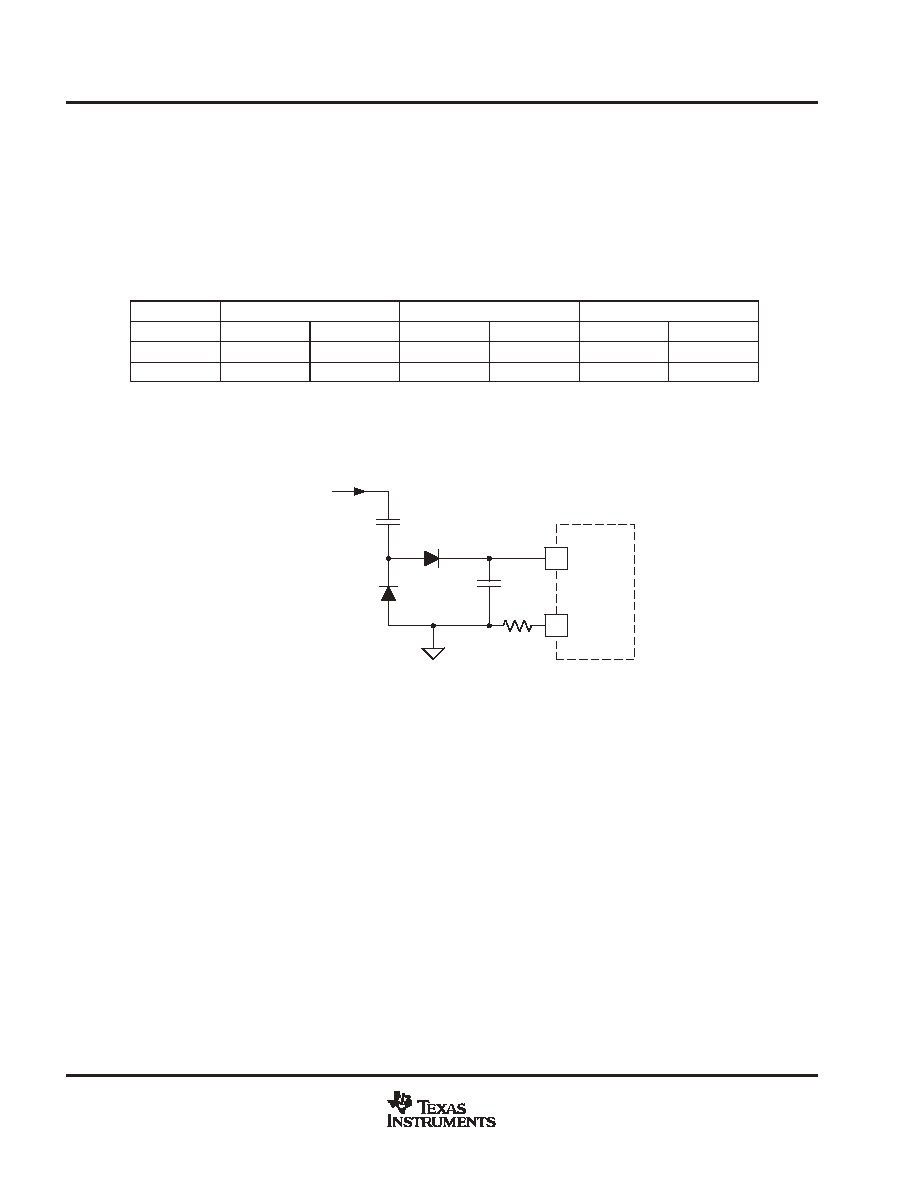
CT
RT
R T
C T
D2
D1
C1
Gate Drive
From Down
Stream PWM
UCC3817A
Figure 7. Synchronizing the UCC3817A to a Down-Stream Converter

UCC2817A, UCC2818A
UCC3817A, UCC3818A
SLUS577A - SEPTEMBER, 2003 - REVISED OCTOBER 2003
19
www.ti.com
APPLICATION INFORMATION
Figure 8
14
12
10
7.45
7.50
7.55
7.60
7.40
VCC - Supply Voltage - V
13
11
9
VREF - Reference V
oltage - V
REFERENCE VOLTAGE
vs
SUPPLY VOLTAGE
Figure 9
REFERENCE VOLTAGE
vs
REFERENCE CURRENT
0
5
10
15
20
25
7.495
7.500
7.505
7.510
7.490
VREF - Reference V
oltage - V
IVREF - Reference Current - mA
Figure 10
MULTIPLIER OUTPUT CURRENT
vs
VOLTAGE ERROR AMPLIFIER OUTPUT
0.0
1.0
2.0
3.0
4.0
5.0
50
200
250
350
0
100
300
150
IAC = 150
�
A
IAC = 300
�
A
IAC = 500
�
A
I MO
UT
-
Multiplier Output Current
-
�
A
VAOUT - Voltage
Error Amplifier
Output - V
Figure 11
MULTIPLIER GAIN
vs
VOLTAGE ERROR AMPLIFIER OUTPUT
1.0
2.0
3.0
4.0
5.0
0.7
1.1
1.3
1.5
0.5
0.9
IAC = 300
�
A
IAC = 500
�
A
IAC = 150
�
A
Multiplier
Gain - K
VAOUT - Voltage
Error Amplifier
Output - V
UCC2817A, UCC2818A
UCC3817A, UCC3818A
SLUS577A - SEPTEMBER, 2003 - REVISED OCTOBER 2003
20
www.ti.com
APPLICATION INFORMATION
Figure 12
VFF - Feedforward Voltage - V
1.0
2.0
3.0
4.0
5.0
100
300
400
500
0
200
VAOUT = 3 V
VAOUT = 2 V
VAOUT = 4 V
VAOUT = 5 V
(VFF
�
I
MO
UT
) -
�
W
MULTIPLIER CONSTANT POWER PERFORMANCE
0.0
References and Resources:
Application Note, Differences Between UCC3817A/18A/19A and UCC3817/18/19, Texas Instruments
Literature Number SLUA294
Evaluation Module, UCC3817EVM, 385V, 250W PFC Boost Converter
User's Guide, UCC3817 BiCMOS Power Factor Preregulator Evaluation Board, Texas Instruments Literature
Number SLUU077
Application Note, Synchronizing a PFC Controller from a Down Stream Controller Gate Drive, Texas
Instruments Literature Number SLUA245
Seminar topic, High Power Factor Switching Preregulator Design Optimization, L.H. Dixon, SEM-700,1990.
Seminar topic, High Power Factor Preregulator for Off-line Supplies, L.H. Dixon, SEM-600, 1988.
Related Products
DEVICE
DESCRIPTION
CONTROL METHOD
TYPICAL POWER LEVEL
UC3854
PFC controller
ACM(2)
200 W to 2 kW+
UC3854A/B
Improved PFC controller
ACM(2)
200 W to 2 kW+
UC3855A/B
High performance soft switching PFC controller
ACM(2)
400 W to 2 kW+
UCC38050/1
Transition mode PFC controller
CRM(1)
50 W to 400 W
UCC3819
Tracking boost PFC controller
ACM(2)
75 W to 2 kW+
UCC28510/11/12/13
Advanced PFC+PWM combo controller
ACM(2)
75 W to 1kW+
UCC28514/15/16/17
Advanced PFC+PWM combo controller
ACM(2)
75 W to 1kW+
NOTES: (1). Critical conduction mode
(2). Average current mode
UCC2817A, UCC2818A
UCC3817A, UCC3818A
SLUS577A - SEPTEMBER, 2003 - REVISED OCTOBER 2003
21
www.ti.com
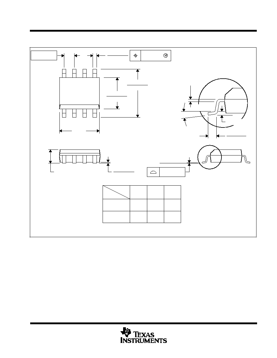
MECHANICAL DATA
D (R-PDSO-G**)
PLASTIC SMALL-OUTLINE PACKAGE
8 PINS SHOWN
8
0.197
(5,00)
A MAX
A MIN
(4,80)
0.189
0.337
(8,55)
(8,75)
0.344
14
0.386
(9,80)
(10,00)
0.394
16
DIM
PINS **
4040047/E 09/01
0.069 (1,75) MAX
Seating Plane
0.004 (0,10)
0.010 (0,25)
0.010 (0,25)
0.016 (0,40)
0.044 (1,12)
0.244 (6,20)
0.228 (5,80)
0.020 (0,51)
0.014 (0,35)
1
4
8
5
0.150 (3,81)
0.157 (4,00)
0.008 (0,20) NOM
0
�
- 8
�
Gage Plane
A
0.004 (0,10)
0.010 (0,25)
0.050 (1,27)
NOTES: A. All linear dimensions are in inches (millimeters).
B. This drawing is subject to change without notice.
C. Body dimensions do not include mold flash or protrusion, not to exceed 0.006 (0,15).

UCC2817A, UCC2818A
UCC3817A, UCC3818A
SLUS577A - SEPTEMBER, 2003 - REVISED OCTOBER 2003
22
www.ti.com
MECHANICAL DATA
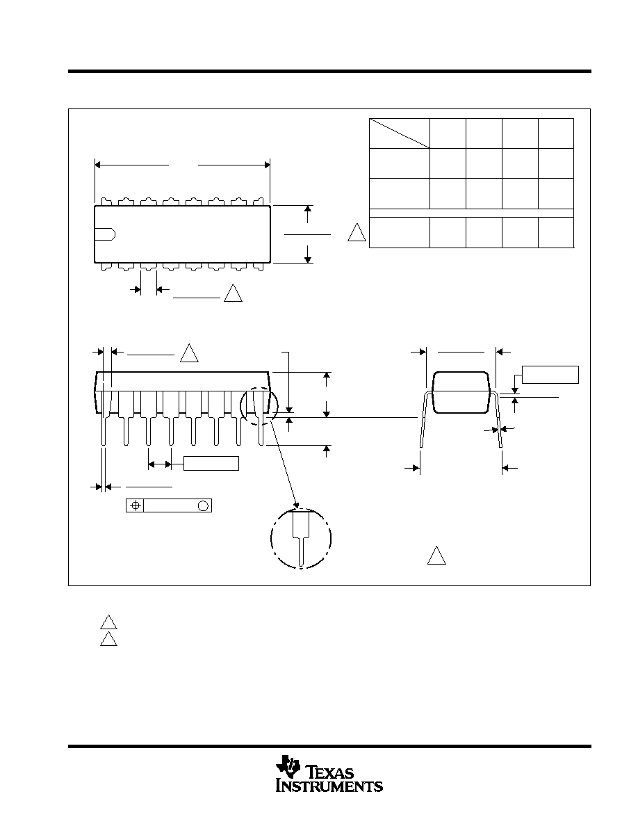
N (R-PDIP-T**)
PLASTIC DUAL-IN-LINE PACKAGE
BB
AC
AD
0.325 (8,26)
0.300 (7,62)
0.010 (0,25) NOM
Gauge Plane
0.015 (0,38)
0.430 (10,92) MAX
20
1.060
(26,92)
0.940
(23,88)
18
0.920
0.850
14
0.775
0.745
(19,69)
(18,92)
16
0.775
(19,69)
(18,92)
0.745
A MIN
DIM
A MAX
PINS **
(23,37)
(21,59)
Seating Plane
14/18 PIN ONLY
20 pin vendor option
4040049/E 12/2002
9
8
0.070 (1,78)
A
0.045 (1,14)
0.020 (0,51) MIN
16
1
0.015 (0,38)
0.021 (0,53)
0.200 (5,08) MAX
0.125 (3,18) MIN
0.240 (6,10)
0.260 (6,60)
M
0.010 (0,25)
0.100 (2,54)
16 PINS SHOWN
MS-100
VARIATION
AA
C
D
D
D
0.030 (0,76)
0.045 (1,14)
NOTES: D. All linear dimensions are in inches (millimeters).
E. This drawing is subject to change without notice.
F. Falls within JEDEC MS-001, except 18 and 20 pin
minimum body lrngth (Dim A).
G. The 20 pin end lead shoulder width is a vendor option,
either half or full width.
UCC2817A, UCC2818A
UCC3817A, UCC3818A
SLUS577A - SEPTEMBER, 2003 - REVISED OCTOBER 2003
23
www.ti.com
MECHANICAL DATA
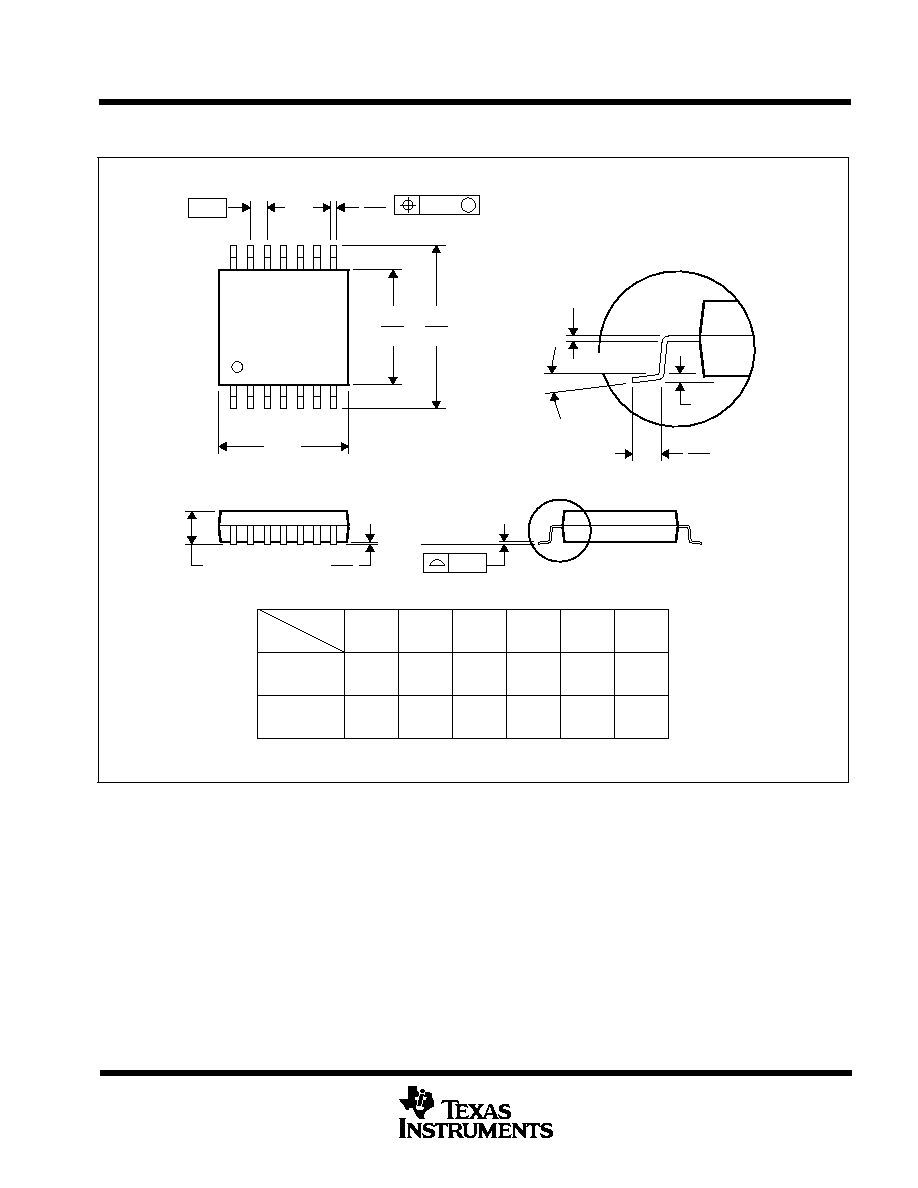
PW (R-PDSO-G**)
PLASTIC SMALL-OUTLINE PACKAGE
14 PINS SHOWN
0,65
M
0,10
0,10
0,25
0,50
0,75
0,15 NOM
Gage Plane
28
9,80
9,60
24
7,90
7,70
20
16
6,60
6,40
4040064/F 01/97
0,30
6,60
6,20
8
0,19
4,30
4,50
7
0,15
14
A
1
1,20 MAX
14
5,10
4,90
8
3,10
2,90
A MAX
A MIN
DIM
PINS **
0,05
4,90
5,10
Seating Plane
0
�
- 8
�
NOTES: H. All linear dimensions are in millimeters.
I. This drawing is subject to change without notice.
J. Body dimensions do not include mold flash or protrusion not to exceed 0,15.
MECHANICAL
MPDI002C � JANUARY 1995 � REVISED DECEMBER 20002
POST OFFICE BOX 655303
�
DALLAS, TEXAS 75265
N (R-PDIP-T**)
PLASTIC DUAL-IN-LINE PACKAGE
BB
AC
AD
0.325 (8,26)
0.300 (7,62)
0.010 (0,25) NOM
Gauge Plane
0.015 (0,38)
0.430 (10,92) MAX
20
1.060
(26,92)
0.940
(23,88)
18
0.920
0.850
14
0.775
0.745
(19,69)
(18,92)
16
0.775
(19,69)
(18,92)
0.745
A MIN
DIM
A MAX
PINS **
(23,37)
(21,59)
Seating Plane
14/18 PIN ONLY
20 pin vendor option
4040049/E 12/2002
9
8
0.070 (1,78)
A
0.045 (1,14)
0.020 (0,51) MIN
16
1
0.015 (0,38)
0.021 (0,53)
0.200 (5,08) MAX
0.125 (3,18) MIN
0.240 (6,10)
0.260 (6,60)
M
0.010 (0,25)
0.100 (2,54)
16 PINS SHOWN
MS-100
VARIATION
AA
C
D
D
D
0.030 (0,76)
0.045 (1,14)
NOTES: A. All linear dimensions are in inches (millimeters).
B. This drawing is subject to change without notice.
C. Falls within JEDEC MS-001, except 18 and 20 pin minimum body lrngth (Dim A).
D. The 20 pin end lead shoulder width is a vendor option, either half or full width.
MECHANICAL DATA
MSOI002B � JANUARY 1995 � REVISED SEPTEMBER 2001
POST OFFICE BOX 655303
�
DALLAS, TEXAS 75265
D (R-PDSO-G**)
PLASTIC SMALL-OUTLINE PACKAGE
8 PINS SHOWN
8
0.197
(5,00)
A MAX
A MIN
(4,80)
0.189
0.337
(8,55)
(8,75)
0.344
14
0.386
(9,80)
(10,00)
0.394
16
DIM
PINS **
4040047/E 09/01
0.069 (1,75) MAX
Seating Plane
0.004 (0,10)
0.010 (0,25)
0.010 (0,25)
0.016 (0,40)
0.044 (1,12)
0.244 (6,20)
0.228 (5,80)
0.020 (0,51)
0.014 (0,35)
1
4
8
5
0.150 (3,81)
0.157 (4,00)
0.008 (0,20) NOM
0
�
� 8
�
Gage Plane
A
0.004 (0,10)
0.010 (0,25)
0.050 (1,27)
NOTES: A. All linear dimensions are in inches (millimeters).
B. This drawing is subject to change without notice.
C. Body dimensions do not include mold flash or protrusion, not to exceed 0.006 (0,15).
D. Falls within JEDEC MS-012
MECHANICAL DATA
MTSS001C � JANUARY 1995 � REVISED FEBRUARY 1999
POST OFFICE BOX 655303
�
DALLAS, TEXAS 75265
PW (R-PDSO-G**)
PLASTIC SMALL-OUTLINE PACKAGE
14 PINS SHOWN
0,65
M
0,10
0,10
0,25
0,50
0,75
0,15 NOM
Gage Plane
28
9,80
9,60
24
7,90
7,70
20
16
6,60
6,40
4040064/F 01/97
0,30
6,60
6,20
8
0,19
4,30
4,50
7
0,15
14
A
1
1,20 MAX
14
5,10
4,90
8
3,10
2,90
A MAX
A MIN
DIM
PINS **
0,05
4,90
5,10
Seating Plane
0
�
� 8
�
NOTES: A. All linear dimensions are in millimeters.
B. This drawing is subject to change without notice.
C. Body dimensions do not include mold flash or protrusion not to exceed 0,15.
D. Falls within JEDEC MO-153

IMPORTANT NOTICE
Texas Instruments Incorporated and its subsidiaries (TI) reserve the right to make corrections, modifications,
enhancements, improvements, and other changes to its products and services at any time and to discontinue
any product or service without notice. Customers should obtain the latest relevant information before placing
orders and should verify that such information is current and complete. All products are sold subject to TI's terms
and conditions of sale supplied at the time of order acknowledgment.
TI warrants performance of its hardware products to the specifications applicable at the time of sale in
accordance with TI's standard warranty. Testing and other quality control techniques are used to the extent TI
deems necessary to support this warranty. Except where mandated by government requirements, testing of all
parameters of each product is not necessarily performed.
TI assumes no liability for applications assistance or customer product design. Customers are responsible for
their products and applications using TI components. To minimize the risks associated with customer products
and applications, customers should provide adequate design and operating safeguards.
TI does not warrant or represent that any license, either express or implied, is granted under any TI patent right,
copyright, mask work right, or other TI intellectual property right relating to any combination, machine, or process
in which TI products or services are used. Information published by TI regarding third-party products or services
does not constitute a license from TI to use such products or services or a warranty or endorsement thereof.
Use of such information may require a license from a third party under the patents or other intellectual property
of the third party, or a license from TI under the patents or other intellectual property of TI.
Reproduction of information in TI data books or data sheets is permissible only if reproduction is without
alteration and is accompanied by all associated warranties, conditions, limitations, and notices. Reproduction
of this information with alteration is an unfair and deceptive business practice. TI is not responsible or liable for
such altered documentation.
Resale of TI products or services with statements different from or beyond the parameters stated by TI for that
product or service voids all express and any implied warranties for the associated TI product or service and
is an unfair and deceptive business practice. TI is not responsible or liable for any such statements.
Following are URLs where you can obtain information on other Texas Instruments products and application
solutions:
Products
Applications
Amplifiers
amplifier.ti.com
Audio
www.ti.com/audio
Data Converters
dataconverter.ti.com
Automotive
www.ti.com/automotive
DSP
dsp.ti.com
Broadband
www.ti.com/broadband
Interface
interface.ti.com
Digital Control
www.ti.com/digitalcontrol
Logic
logic.ti.com
Military
www.ti.com/military
Power Mgmt
power.ti.com
Optical Networking
www.ti.com/opticalnetwork
Microcontrollers
microcontroller.ti.com
Security
www.ti.com/security
Telephony
www.ti.com/telephony
Video & Imaging
www.ti.com/video
Wireless
www.ti.com/wireless
Mailing Address:
Texas Instruments
Post Office Box 655303 Dallas, Texas 75265
Copyright
2003, Texas Instruments Incorporated