SLUS390 - MARCH 1998
FEATURES
∑
Compatible with Voltage or Current
Mode Control Methods
∑
Practical Operation at Switching
Frequencies to 4MHz
∑
50ns Propagation Delay to Output
∑
High Current Complementary
Outputs
∑
Programmable Dead Time and
Frequency Oscillator
∑
Pulse by Pulse Current Limiting
∑
Latched Overcurrent Comparator
with Full Cycle Restart
∑
Programmable Undervoltage
Lockout (UVLO)
∑
Adjustable Blanking for Leading
Edge Noise Tolerance
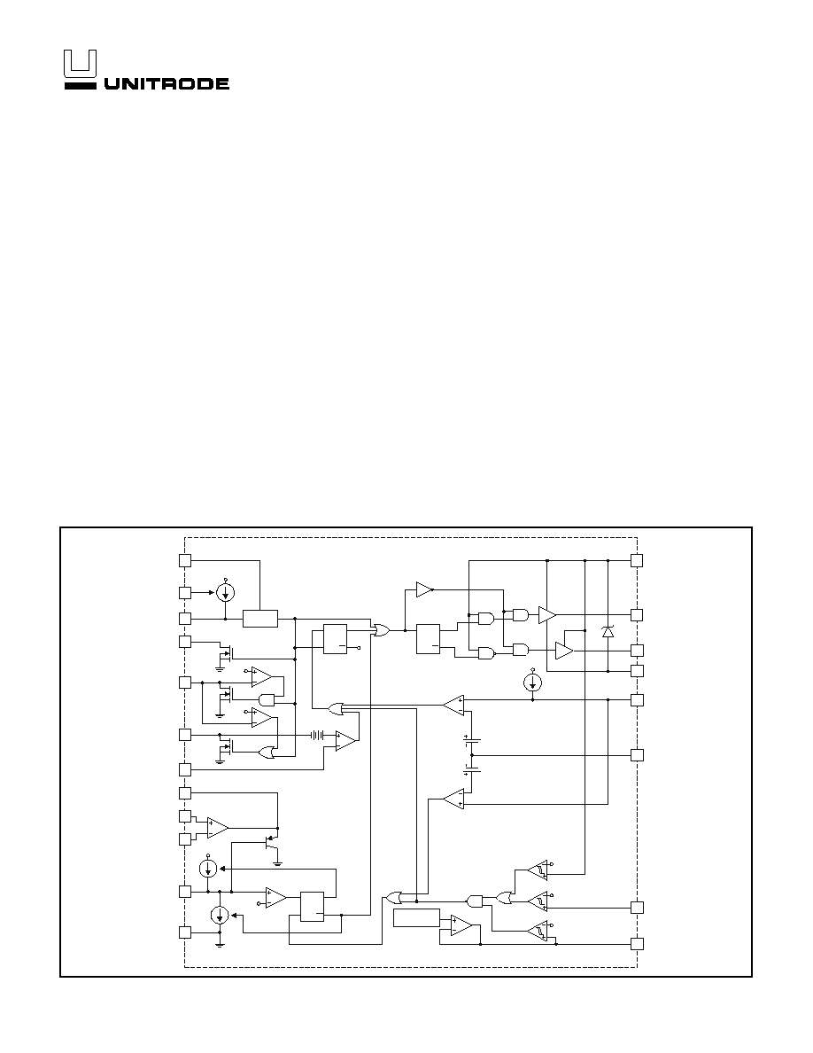
High Speed PWM Controller
UDG-98043
UCC1829-1/-2/-3
UCC2829-1/-2/-3
UCC3829-1/-2/-3
PRELIMINARY
DESCRIPTION
The UCC3829 is a BiCMOS High Speed PWM Controller IC. It is opti-
mized for high frequency switched mode power supply applications. The
IC can be used in both voltage mode and current mode control applica-
tions. Care was given to minimizing the propagation delays through the
comparators and logic circuitry while maximizing the bandwidth and slew
rate of the error amplifier. The oscillator frequency and deadtime can be
programmed via two external resistors and a capacitor. The undervolt-
age lockout threshold can be programmed using an external resistor di-
vider. The current limit and overcurrent threshold can be set externally.
The IC is available in push-pull (-1), single ended (-2), or complementary
(-3) output configuration.
Fault protection circuitry includes undervoltage detection for the internal
bias supply, and overcurrent detection. The fault detection logic sets a
latch that ensures full discharge of the soft start capacitor before allowing
a restart. While the fault latch is set, the outputs are in a low state. In the
event of continuous faults, the soft start capacitor is fully charged before
discharging to insure that the fault frequency does not exceed the de-
signed soft start period.
15
13
18
14
18
VDD
PGND
OUTA
OUTB
GND
10
SS
S
R
D
Q
Q
1V
2
INV
1
NINV
V
BIAS
3
EAOUT
5
RAMP
4
19
LEB
1.5V
1.2V
4V
6
RT2
7
CT
CLOCK
V
BIAS
8
RT1
9
BISYNC
S
R
Q
Q
T
>
Q
Q
V
BIAS
1.25V
0.9V
3V
REFERENCE
11
23
17
VREF
CL≠
UVLO
2.1V
3V/2.5V
14.2V/9V
12
CL+
PWCONT
BLOCK DIAGRAM
2
UCC1829-1/-2/-3
UCC2829-1/-2/-3
UCC3829-1/-2/-3
GND
LEB
VREF
UVLO
VDD
OUTB
OUTA
PGND
1
2
3
4
5
6
7
8
20
19
18
17
16
15
14
13
INV
NINV
RT1
RT2
CT
EAOUT
PWCONT
RAMP
9
10
SS
BISYNC
CL≠
CL+
12
11
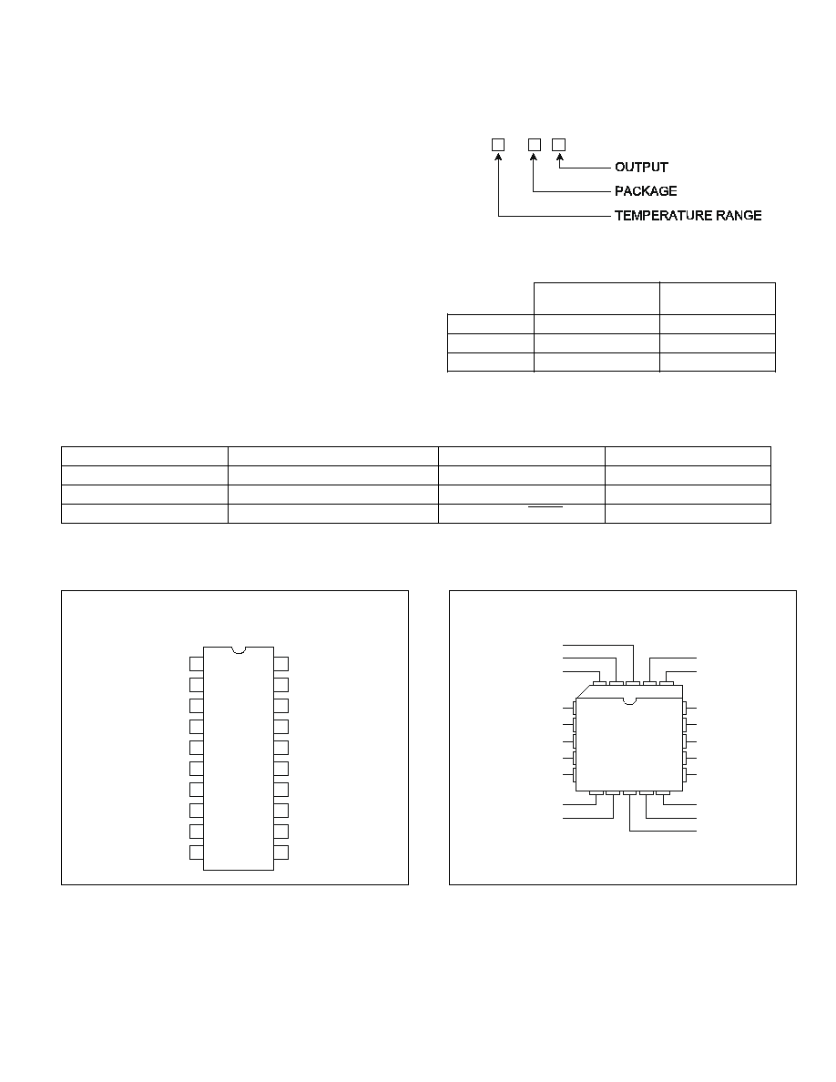
CONNECTION DIAGRAMS
DIL-20, SOIC-20 (Top View)
N, DW and J Packages
ABSOLUTE MAXIMUM RATINGS
Supply Voltage . . . . . . . . . . . . . . . . . . . . . . . . . . . . . . . . . . 15V
Supply Current . . . . . . . . . . . . . . . . . . . . . . . . . . . . . . . . . 25mA
Output Current (OUTA, OUTB, PGND, VCC)
DC . . . . . . . . . . . . . . . . . . . . . . . . . . . . . . . . . . . . . . . . . 0.5A
Pulsed (0.5
µ
sec) . . . . . . . . . . . . . . . . . . . . . . . . . . . . . . 2.2A
PGND. . . . . . . . . . . . . . . . . . . . . . . . . . . . . . . . . . . . . . . .
±
0.2V
Analog Inputs
INV, NINV, RAMP, SS . . . . . . . . . . . . . . . . . . . . . ≠0.3 to 7V
CL+, CL-. . . . . . . . . . . . . . . . . . . . . . . . . . . . . . . . 0.3V to 3V
Error Amplifier Output Current . . . . . . . . . . . . . . . . . . . . . . 5mA
Error Amplifier Output Capacitance . . . . . . . . . . . . . . . . . . 20pF
Storage Temperature . . . . . . . . . . . . . . . . . . . ≠65∞C to +150∞C
Junction Temperature . . . . . . . . . . . . . . . . . . . ≠55∞C to +150∞C
Lead Temperature (Soldering, 10sec.) . . . . . . . . . . . . . +300∞C
Unless otherwise indicated, voltages are referenced to GND.
Currents are positive into, negative out of the specified terminal.
Consult Packaging Section of Databook for thermal limitations
and considerations of packages.
UCC
829
≠
ORDERING INFORMATION
PLCC-20 (Top View)
Q Package
PART VERSION TABLE
PART NUMBER
OUTPUT
OUT A/B PHASE
OUTPUT FREQUENCY
UCCX829-1
Push-Pull
180∞ Out of Phase
F
CT
/2
UCCX829-2
Dual Single-Ended
In Phase
F
CT
UCCX829-3
Non-Overlapping Complimentary
OUTB = OUTA
F
CT
3
18
17
16
NINV
1
2
20 19
15
14
4
5
6
7
8
9
11
10
12 13
INV
EAOUT
VREF
LEB
GND
UVLO
VDD
OUTA
OUTB
PWCONT
RAMP
RT2
CT
RT1
PGND
CL≠
CL+
BISYNC
SS
TEMPERATURE & PACKAGE SELECTION
GUIDE TABLE
TEMPERATURE
RANGE
AVAILABLE
PACKAGES
UCC1829-X
≠55∞C to +125∞C
J
UCC2829-X
≠40∞C to +85∞C
N, DW, Q
UCC3829-X
0∞C to +70∞C
N, DW, Q
3
UCC1829-1/-2/-3
UCC2829-1/-2/-3
UCC3829-1/-2/-3
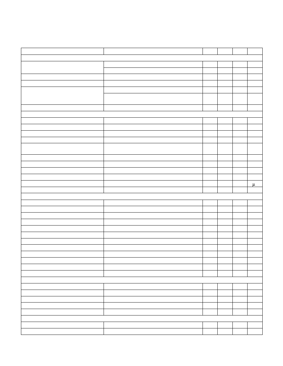
ELECTRICAL CHARACTERISTICS:
Unless otherwise specified, RT1 = 34.8k
, CT = 470pF, RT2 = 392
, VDD = 12V,
Over Full Temperature Range and T
A
= T
J
.
PARAMETER
TEST CONDITIONS
MIN
TYP
MAX
UNITS
Reference Section
Output Voltage
T
J
= 25∞C, No Load, Output Off
2.97
3
3.03
V
Over Temperature, No Load, Output Off
2.94
3.06
V
Line Regulation
VDD = 5V to 14.5V, Output Off, No Load, (Note 2)
35
50
mV
Load Regulation
0 < I
REF
< 5mA
2
10
mV
Total Output Variation
Line, Load, Temperature = 0∞C to 70∞C, (Note 1)
2.93
3.07
V
Line, Load, Temperature = ≠55∞C to +125∞C,
(Note 1)
2.90
3.10
V
Short Circuit Current
VREF = 0
≠25
mA
Oscillator Section
Initial Accuracy
T
J
= 25∞C
360
400
440
kHz
Total Variation
Line, Temperature (Note 1)
320
480
kHz
Temperature Stability
T
MIN
< T
A
< T
MAX
(Note 1)
5
10
%
Initial Accuracy, 1MHz
RT1 = 25.7k, CT = 150pF, T
J
= 25∞C, (Note 1)
0.9
1
1.1
MHz
Total Variation, 1MHz
RT1 = 25.7k, CT = 150pF, Line, Temperature
(Note 1)
0.8
1.2
MHz
Ramp Peak Voltage
1.8
2
2.2
V
Ramp Valley Voltage
1
1.5
V
Peak To Peak Voltage
0.85
1
1.15
V
BISYNC Output Source Current
V
BISYNC
= VDD ≠ 0.5V
≠2
≠1.5
mA
BISYNC Output Sink Current
V
BISYNC
= 0.5V
60
140
A
BISYNC Input Threshold
1
1.5
2
V
Error Amplifier Section
Input Offset Voltage
5
mV
Input Bias Current
≠1
1
µ
A
Input Offset Current
250
nA
Open Loop Gain
70
80
dB
CMRR
1.5V < VCM < 4.5V
75
dB
PSRR
5V < VDD < 14.5V
75
dB
Output Sink Current
V
EAOUT
= 1V
300
500
µ
A
Output Source Current
V
EAOUT
= 4V
≠500
≠300
µ
A
Output High Voltage
I
EAOUT
= ≠300
µ
A
3
5
V
Output Low Voltage
I
EAOUT
= 300
µ
A
0.6
1
V
Gain Bandwidth Product
VDD = 12V, T
J
= 25∞C
5
7
MHz
Slew Rate
1.5
2
V/
µ
s
PWM Comparator Section
Input Bias Current V(RAMP)
≠60
1
µ
A
Minimum Duty Cycle
400kHz
0
%
Maximum Duty Cycle (UCCX829-1)
400kHz, RT2 Resistor = 200
42.5
%
Maximum Duty Cycle (UCCX829-2, -3)
400kHz, RT2 Resistor = 200
85
%
Delay to Output
50
100
ns
Current Limit Fault Section
Soft Start Charge Current
≠40
≠10
µ
A
Soft Start Complete Threshold
SS Pin (Note 1)
3
V
4
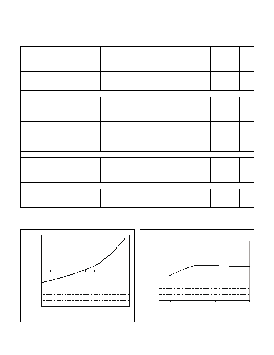
UCC1829-1/-2/-3
UCC2829-1/-2/-3
UCC3829-1/-2/-3
ELECTRICAL CHARACTERISTICS:
Unless otherwise specified, RT1 = 34.8k
, CT = 470pF, RT2 = 392
, VDD = 12V,
Over Full Temperature Range and T
A
= T
J
.
PARAMETER
TEST CONDITIONS
MIN
TYP
MAX
UNITS
Restart Discharge Current
10
40
µ
A
Restart Threshold
0.8
1
1.2
V
Current Limit Threshold
Relative to CL≠
0.8
0.875
1.1
V
Overcurrent Threshold
Relative to CL≠
1.1
1.25
1.4
V
Current Limit Delay to Output
50
100
ns
V
DD
= 5V
100
400
ns
Output Section (OUTA, OUTB)
Output Low Saturation
I
OUT
= 200mA
0.5
1.0
V
Output High Saturation
I
OUT
= ≠100mA
0.5
1.0
V
UVLO Output Low Saturation
At 10mA
0.1
0.5
V
Rise Time
C
LOAD
= 1nF, TJ = 25∞C
20
40
ns
Fall Time
C
LOAD
= 1nF, TJ = 25∞C
10
20
ns
Output Source Current
V
OUT
= 0, TJ = 25∞C (Note 1)
≠0.75
A
Output Sink Current
V
OUT
= 12V, TJ = 25∞C (Note 1)
1.5
A
Complementary Delay Time (Delay 2)
(UCCX829 -3 Only)
(Note 1)
50
150
ns
Undervoltage Lockout
UVLO Enable Threshold
2.9
3
3.1
V
UVLO Hysteresis
0.3
0.5
0.7
V
VDD UVLO Enable Threshold
13.5
14.5
V
VDD UVLO Hysteresis
3.5
7
V
Supply Section
VDD Range
No Load
4.25
14.5
V
Startup Current
V
UVLO
= 2V, V
DD
= 13.5V
3
5
mA
IDD
400kHz, No Load
8
12
mA
Note 1: Guaranteed by design. Not 100% tested in production.
Note 2: Refer to Figure 1.
2.970
2.975
2.980
2.985
2.990
2.995
3.000
3.005
3.010
3.015
3.020
3.025
3.030
5.0
6.0
7.0
8.0
9.0
10.0
11.0
12.0
13.0
14.0
15.0
V
DD
[V]
VREF
[V]
Figure 1. Reference vs. V
DD
TYPICAL CHARACTERISTIC CURVES
2.95
2.96
2.97
2.98
2.99
3
3.01
3.02
3.03
3.04
3.05
-75
-50
-25
0
25
50
75
100
125
TEMPERATURE [∞C]
V
REF
[V]
Figure 2. Reference vs. Temperature

5
UCC1829-1/-2/-3
UCC2829-1/-2/-3
UCC3829-1/-2/-3
PIN DESCRIPTIONS
BISYNC: Combination clock output/sync input pin. The
clock signal can be viewed on this pin. If BISYNC is con-
nected to BISYNC of other UCC3829 chips, all the oscil-
lators will run at the highest of all the chips frequencies.
The BISYNC pin has a weak pull down and a strong pull
up.
CL+: Current sense input for current limiting. The CL+
and CL- pins are used for current sensing. CL+ is the
current signal while CL- is the kelvin return for the sens-
ing function.
CL≠: Current sense input kelvin common.
CT: Oscillator timing capacitor. A capacitor connected
between CT and GND is charged by a current source
controlled by RT1. The capacitor is discharged through a
resistor connected between CT and RT2.
EAOUT: Error amplifier output. This output is normally
connected directly to the PWCONT pin. It can also be
connected to PWCONT through a resistor divider at-
tenuation network to allow more swing of the error ampli-
fier output. A maximum capacitive load of 20pF with
respect to ground must be observed to insure stability of
the error amplifier.
GND: Logic and analog ground. The GND pin should be
used for all signal level returns, except the current sense
inputs.
INV: Error amplifier inverting input.
LEB: Leading edge blanking programming pin. Connect-
ing a resistor between VREF and LEB and a capacitor
between LEB and GND will program a leading edge
blanking time according to the RC of the resistor/capaci-
tor combination. Connecting the LEB pin to VDD disables
the Leading Edge Blanking function.
NINV: Error amplifier non-inverting input.
OUTA: Output A. The OUTA pin will pull down with ap-
proximately 1.5A and pull up with approximately 0.75A.
The UCC3829-1 implements push-pull outputs with
OUTA and OUTB active on alternating clock cycles. The
UCC3829-2 implements OUTA and OUTB being in
phase. The UCC3829 -3 implements OUTA and OUTB to
be non-overlapping complementary outputs during the
same
clock
cycle.
The
output
frequency
of
the
UCC3829-1 is half that of the UCC3829-2
and
UCC3829 -3.
OUTB: Output B. The OUTB pin will pull down with ap-
proximately 1.5A and pull up with approximately 0.75A.
The UCC3829-1 implements push-pull outputs with
OUTA and OUTB active on alternating clock cycles. The
UCC3829-2 implements OUTA and OUTB being in
phase. The UCC3829 -3 implements OUTA and OUTB
to be non-overlapping complementary outputs during the
same
clock
cycle.
The
output
frequency
of
the
UCC3829-1 is half that of the UCC3829-2
and
UCC3829 -3.
PGND: Power ground return. The PGND pin should be
used as the return for the VDD bypass capacitor and the
current sense kelvin CL-.
PWCONT: Pulse width control input. This is connected to
the PWM comparator inverting input.
RAMP: Ramp input . This is connected to the PWM com-
parator non-inverting input through a level shifting volt-
age of approximately 1.25V.
RT1: Oscillator charging current programming resistor. A
1V reference at this pin generates a current through a re-
sistor connected between RT1 and GND. This current is
mirrored and ratioed to charge the timing capacitor con-
nected to pin CT.
RT2: Oscillator discharge time programming resistor. The
oscillator (and output) dead time can be programmed via
this pin. The discharge of the timing capacitor C
T
is de-
termined by an RC discharge using a resistor connected
between RT2 and C
T
.
SS: Soft start capacitor pin. A capacitor connected to SS
determines the time the IC takes to soft start. The nomi-
nal SS pin pull up and pull down current is 20
µ
A. The soft
start time delay is approximately calculated as:
CSS ∑ 3V
20 A
µ
when charging from 0V. After the SS pin reaches the SS
complete threshold of 3V, another SS cycle can be
started. The restart time is approximately:
2 ∑ CSS ∑ 3V
20 A
µ
UVLO: Undervoltage lockout programming pin. Connect-
ing a resistor divider between VDD, UVLO, and GND
sets a VDD value at which the UCC3829 chip will be en-
abled. When the voltage on the UVLO pin reaches 3V,
the chip is enabled. When the voltage on UVLO falls be-
low 2.5V, the chip is disabled.
VDD: Voltage supply to IC. VDD is clamped at 14V.
VREF: Voltage reference output and filtering. The voltage
reference output appears on the VREF pin. It is buffered
to drive approximately 5mA and short circuit protected at
approximately 25mA. A bypass capacitor of at least
0.1
µ
F must be connected from VREF to ground.
6
UCC1829-1/-2/-3
UCC2829-1/-2/-3
UCC3829-1/-2/-3
APPLICATION INFORMATION
Functional Programmability
Various features of the UCC3829 are user programma-
ble. RT1 and RT2 allow independent programming for
oscillator rise and fall times within the normal operational
range of the chip. A new feature allows the user to pro-
gram the voltage that flags an undervoltage fault. The
default value of 14V for chip turn-on is selected by tying
the UVLO pin to ground.
If the user wants to select
startup voltage then a resistive divider should be tied
from Vdd to ground, with the centerpoint tied to the
UVLO pin. The chip will be enabled when the UVLO pin
reaches 3V, and disabled below 2.5V.
Leading edge
blanking can also be optimized to eliminate turn-on noise
when current mode control is used or disabled when de-
sired.
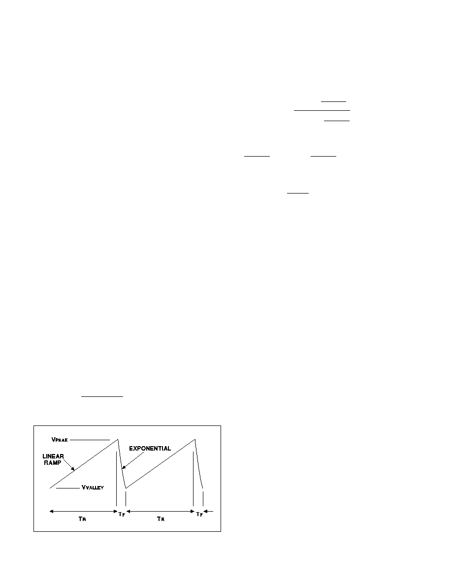
Oscillator
The oscillator uses an external capacitor C
T
and two ex-
ternal resistors R
T1
and R
T2
to generate the clock fre-
quency and dead time. A precise reference voltage is
placed across resistor R
T1
to generate a current refer-
ence. The current is then mirrored and used to charge
the capacitor C
T
from V
VALLEY.
When a "peak" threshold
is reached, an on chip MOSFET connects the RT2 pin to
GND, discharging CT to a "valley" threshold through an
external resistor R
T2
. The CT waveform has a linear
ramp shape while charging and an exponential (RC)
slope while discharging. The slope of the charging ramp
is set by the C
T
, R
T1
combination and the slope of the
discharging ramp is set by the values of C
T
and R
T2
.
The approximate equation for the rising edge (T
R
) of the
C
T
waveform (maximum on-time period) is:
T
C R
V
V
R
T
T
PEAK
VALLEY
=
1
9 3
≠
.
The approximate equation for the falling edge (T
F
) of the
C
T
waveform (deadtime period) is:
T
R C
V
R
R
V
R
R
F
T
T
PEAK
T
T
VALLEY
T
T
=
=
2
2
1
2
1
9 3
9 3
ln
≠
.
≠
.
Assuming that:
9 3
9 3
2
1
2
1
.
.
R
R
V
R
R
V
T
T
PEAK
T
T
VALLEY
<<
<<
and
We get a simplified equation:
T
R C
V
V
F
T
T
PEAK
VALLEY
=
2
ln
Given a maximum on-time and frequency and assuming
an initial value for either R
T2
or C
T
, you can use the T
F
equation to calculate the other. Once you have a value
for C
T
, you can calculate R
T1
using the T
R
equation.
Error Amplifier Section
The Error Amplifier has both inputs and the output
brought out to pins NINV, INV, and EAOUT. The output of
the error amplifier can be connected to the inverting input
of the PWM comparator via the pin PWCONT. This al-
lows inserting attenuation which enables using the full
output swing of the error amplifier. The output of the error
amplifier is forced to follow the soft start waveform during
soft start.
PWM and Output Section
The non-inverted input of the PWM comparator is con-
nected to RAMP. The RAMP can be connected to either
the C
T
capacitor for voltage mode control, to the current
sense resistor for current mode control, or to a feed for-
ward capacitor for input voltage feed forward control. The
C
T
waveform can be coupled to RAMP to provide slope
compensation in the current mode case. The MOSFET
switch connected to RAMP provides for the discharge of
the feedforward capacitor. There is a short time constant
(3ns) filter across the inputs of the PWM comparator to
reduce noise.
The output of the PWM comparator feeds an OR gate
which, together with several other fault signals, sets the
PWM latch. The latch is in turn reset on every dead time
period of the clock waveform. The output of the PWM
latch is OR'ed with the clock and the output of the Fault
Latch (described below) to feed into the pulse steering
Toggle Flip-Flop (TFF). The resulting signal is then
steered
according
to
the
output
configuration
of
UCC3829. The clock output becomes the deadtime be-
tween the outputs.
Figure 3.
UDG-97016
7
UCC1829-1/-2/-3
UCC2829-1/-2/-3
UCC3829-1/-2/-3
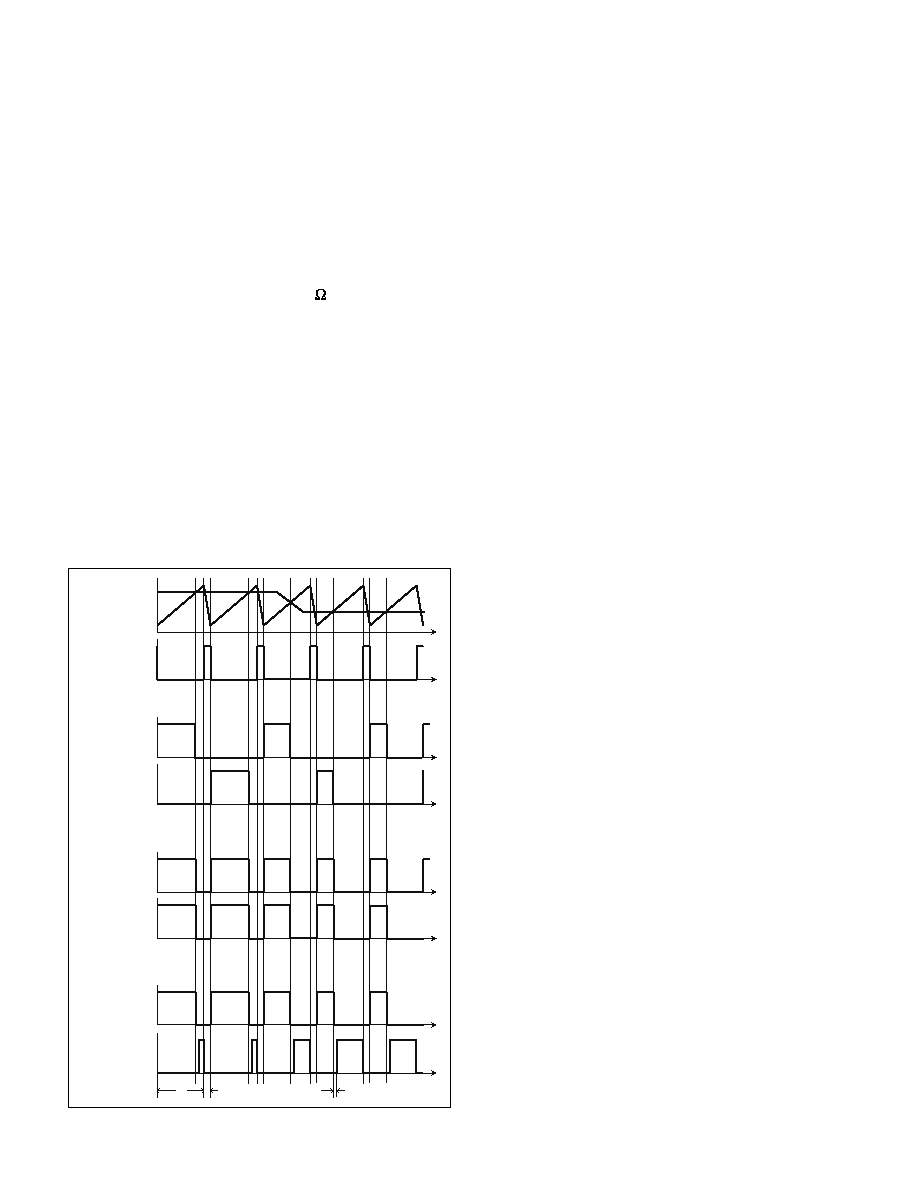
Output Timing Configurations
The timing diagram shows the major differences between
the UCC3829-1, -2 and -3 parts.
The output of the
UCC3829-1 is a push-pull configuration with outputs A
and B 180∞ out of phase and with an output frequency
that is half of the C
T
's waveform.
The UCC3829-2 produces dual outputs that are in phase
and can be used in situations that require high current
drive for single ended designs. A 0.5
resistor should be
added in series with each output before they are con-
nected together. The output pulse frequency is equal to
the CT waveform frequency in this case.
The output drive in the UCC3829-3 has a non-
overlapping complementary configuration. During each
clock cycle Output A produces an output pulse, followed
by a short delay, and then Output B produces an output
pulse. The short delay between Output A and Output B
pulses is tcd, the complementary delay time. This en-
sures that the outputs are never high simultaneously.
Leading Edge Blanking Section
The Leading Edge Blanking circuit provides a means to
insert a blanking period at the beginning of the cycle,
providing noise pulse elimination for current mode control
applications. This feature is similar to that of the UC3825
and UC3823A/B controllers. When enabled, an external
resistor is connected from LEB to VREF. An external ca-
pacitor is connected from LEB to either VREF or GND.
During the deadtime, LEB is pulled to GND. At the begin-
ning of the cycle, the pin is released and the capacitor
charges through the resistor toward VREF. At the thresh-
old VREF/2, a comparator senses the voltage and LEB is
removed. The leading edge blanking function can be dis-
abled by connecting LEB to VDD (> VREF). Leading
edge blanking is performed by the same MOSFET switch
connected to RAMP that is used for voltage feed forward
operation.
Current Timing and Protection
The current limit and overcurrent functions are accom-
plished using the pins CL+ and CL≠. These two pins pro-
vide for differential current level sensing, with the trip
points referenced to CL≠, rather than GND. The current
limit function provides a pulse by pulse current limiting,
whereas the overcurrent function is considered a fault
condition and initiates a fault logic soft start cycle.
The UCC3829 utilizes differential current sensing and
separate logic and power ground pins to eliminate some
of the noise issues of using current mode control. De-
vices with only one common ground pin for all stated
functions required the combination of power gate drive
current and low-level sensing currents in a common
trace. Since the current signal needed for control is em-
bedded in the power gate drive current, it is not enough
just to separate logic and power ground pins. Differential
sensing in UCC3829 referenced to the negative rail al-
lows the cleanest method of sensing current for use in a
peak current mode controlled power supply utilizing re-
sistive sensing. Current limiting is done on a cycle by cy-
cle basis when the typical threshold of 0.875V is
reached. If the fault level of 1.25V is reached a soft start
cycle is initiated. Internal circuitry insures that soft start
cycles are completed so that fault currents can be con-
trolled.
Fault Logic Section
The fault logic detects and handles various fault condi-
tions in the system. The output of the overcurrent com-
parator is logically ORed with the output combination of
the undervoltage detection circuit ORed with the output
of the VREF good circuit. The output of the precision ref-
erence voltage VREF is compared to a level (approxi-
tr
tf
tcd
UCC1829-3
OUT A
UCC 1829-3
OUT B
UCC1829-2
OUT B
UCC1829-2
OUT A
UCC1829-1
OUT B
UCC1829-1
OUT A
PWM CNTL
CT
BISYNC
TIMING DIAGRAMS
8
UCC1829-1/-2/-3
UCC2829-1/-2/-3
UCC3829-1/-2/-3
mately 3 V
BE
voltages) to determine if the reference is
alive. The undervoltage circuit either uses a user pro-
grammed level with a 16% hysteresis or an on threshold
equal to the V
DD
clamp voltage and an off threshold of
9V.
Once a fault occurs, a soft start cycle takes place. A fault
sets the fault latch. The Q output of the fault latch sets
the RS delay latch and turns on the 20
µ
A soft start dis-
charge current sink. The Q output of the fault latch is
gated, however, by the output of the S
S
complete com-
parator. This insures that a SS cycle cannot start before
the previous one has finished. The soft start capacitor
then is discharged to 1V which is sensed by the R
S
delay
comparator. The fault latch is then reset. This in turn re-
sets the R
S
delay latch and turns off the 20
µ
A current
sink and turns on a 20
µ
A current source to charge the S
S
capacitor.
The under voltage detection is set to a default value of
14V turn on (V
DD
clamp active value) and 9V turn off
when the UVLO pin is tied to GND. This default configu-
ration can be overridden by connecting a resistor divider
between V
DD
and GND to the UVLO pin. The hysteresis
for the user set threshold is 16%.
During undervoltage lockout, the self biasing outputs are
held "OFF" to prevent accidental turn-on of the power
switches.
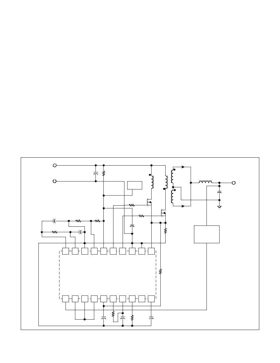
Supply Section
The incoming voltage supply V
DD
is clamped by a shunt
V
DD
Clamp circuit at 14V.
V
IN
V
OUT
NINV
INV
EAO
U
T
PWCONT
RAM
P
RT
2
CT
RT
1
BI
SYNC
SS
1
2
3
20
19
4
5
6
7
8
9
10
11
12
14
15
16
17
18
13
CL
+
CL
-
PG
ND
OUT
B
OUT
A
VD
D
UVL
O
GND
LE
B
VR
EF
UCC3829-1
ISOLATED
FEEDBACK
DC SOURCE
OR RECTIFIED AC
BIAS
SUPPLY
TYPICAL APPLICATIONS
Figure 4. Push-Pull Converter Using UCC3829-1
UDG-98013
9
UCC1829-1/-2/-3
UCC2829-1/-2/-3
UCC3829-1/-2/-3
V
IN
V
OUT
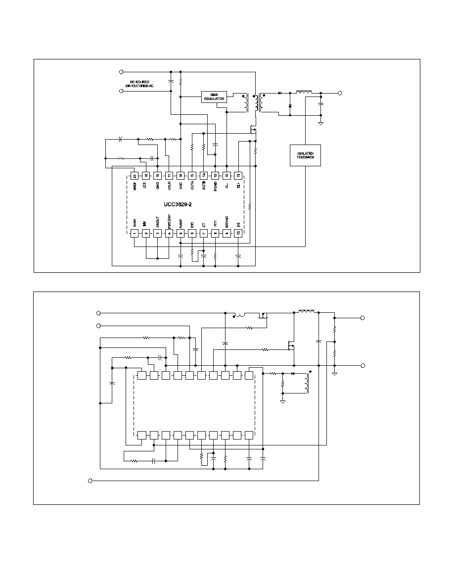
TYPICAL APPLICATIONS (cont.)
Figure 5. Single Ended Converter with High Power Gate Drive Using UCC3829-2
UDG-98014
NINV
INV
EAO
UT
PWCONT
RAM
P
RT
2
CT
RT
1
BI
SYNC
SS
1
2
3
20
19
4
5
6
7
8
9
10
11
12
14
15
16
17
18
13
CL
+
CL
-
PG
ND
OUT
B
OUT
A
VDD
UVL
O
GND
LE
B
VREF
UCC3829-3
V
IN
V
DD
SUPPLY
P/O CT1
P/O CT1
V
OUT
COMMON
Figure 6. Synchronous Rectifier Controller Using UCC3829-3
UDG-98015
For additional information, please see U-128 that details
operation and application of some of the features of
UC3823A,B and UC3825A,B PWM Controllers.
UNITRODE CORPORATION
7 CONTINENTAL BLVD. ∑ MERRIMACK, NH 03054
TEL. (603) 424-2410 ∑ FAX (603) 424-3460

IMPORTANT NOTICE
Texas Instruments and its subsidiaries (TI) reserve the right to make changes to their products or to discontinue
any product or service without notice, and advise customers to obtain the latest version of relevant information
to verify, before placing orders, that information being relied on is current and complete. All products are sold
subject to the terms and conditions of sale supplied at the time of order acknowledgment, including those
pertaining to warranty, patent infringement, and limitation of liability.
TI warrants performance of its semiconductor products to the specifications applicable at the time of sale in
accordance with TI's standard warranty. Testing and other quality control techniques are utilized to the extent
TI deems necessary to support this warranty. Specific testing of all parameters of each device is not necessarily
performed, except those mandated by government requirements.
Customers are responsible for their applications using TI components.
In order to minimize risks associated with the customer's applications, adequate design and operating
safeguards must be provided by the customer to minimize inherent or procedural hazards.
TI assumes no liability for applications assistance or customer product design. TI does not warrant or represent
that any license, either express or implied, is granted under any patent right, copyright, mask work right, or other
intellectual property right of TI covering or relating to any combination, machine, or process in which such
semiconductor products or services might be or are used. TI's publication of information regarding any third
party's products or services does not constitute TI's approval, warranty or endorsement thereof.
Copyright
©
2000, Texas Instruments Incorporated