 | –≠–ª–µ–∫—Ç—Ä–æ–Ω–Ω—ã–π –∫–æ–º–ø–æ–Ω–µ–Ω—Ç: UCC3831DW | –°–∫–∞—á–∞—Ç—å:  PDF PDF  ZIP ZIP |
11/97
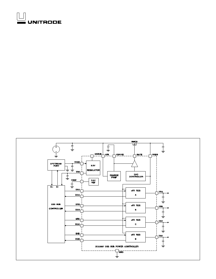
APPLICATION AND BLOCK DIAGRAM
∑
Fully USB Compliant
∑
Support Four 5V Peripherals and
One USB 3.3V Controller
∑
Separate Power Enables
∑
500mA Current Limiting per
Channel
∑
Separate Open Drain Fault
Indicator for Each Channel
∑
3.3V Output for USB Controller
∑
Available in 28 Pin Wide Surface
Mount and DIP
Universal Serial Bus Power Controller
FEATURES
DESCRIPTION
UCC3831
PRELIMINARY
UDG-97101
The UCC3831 Power Controller is designed to provide a self powered
USB hub with a local 3.3V regulated voltage and four 5V regulated volt-
ages for USB ports. Each of the 5V output ports is individually enabled
for optimal port control. Each port also provides an overcurrent fault sig-
nal indicating that the port has exceeded a 500mA current limit. The
3.3V linear regulator is used to power the local USB microcontroller.
This regulator is protected with a 100mA current limit and has a logic
level enable input.
The UCC3831 can be configured to provide USB port power from a
loosely regulated voltage such as a Filament voltage internal to a moni-
tor. Pre-regulation is provided by an internal linear regulator controller
and one external logic level N-channel MOSFET. The UCC3831 can
also be configured without using the pre-regulator stage by connecting
the VREG pins to a regulated 5.5V 2A source.
The UCC3831 comes in a 28-pin wide SOIC power package optimized
for power dissipation, and is protected by internal over-temperature
shutdown mechanism, which disables the outputs should the internal
junction temperature exceed 150∞C.
2
UCC3831
PARAMETER
TEST CONDITIONS
MIN
TYP
MAX
UNITS
Input Supply Currents
VHUB Supply Current
No External Load on V33
1
3
mA
VFIL Supply Current
1
3
mA
Reference
VREF Voltage
Over Temperature
2.35
2.5
2.65
V
Line Regulation
VHUB = 4.5V to 9V
3
10
mV
3.3V Regulator
V33 Voltage
T
J
= 25∞C, I
LOAD
= 10mA
3.2
3.3
3.4
V
0mA to 100mA, 0∞C to 125∞C, VHUB = 4.5V to 9V
3.165
3.3
3.435
V
Short Circuit Current Limit
VHUB = 6V, Output shorted to Ground
100
120
150
mA
Pre-Regulator
VREG Voltage
0A to 2A, 0∞C to 125∞C, VFIL = 6V to 9V
5.25
5.5
5.7
V
5V Regulator
V5A-D Voltage
T
J
= 25∞C, I
LOAD
= 250mA, V
REG
= 5.5V
4.85
5
5.15
V
0mA to 500mA, 0∞C to 125∞C
4.8
5
5.2
V
Short Circuit Current Limit
VREG = 5.5V, Output Shorted to Ground
500
600
750
mA
Charge Pump
Quiescent Output Voltage
T
J
= 25∞C, VFIL = 6V, ENA-D = 5V, ENHUB = 5V
11
11.45
12
V
0∞C to 125∞C, VFIL = 6V
10.5
11.45
12
V
Output Impedance
9
15
k
Enable Inputs
ENA-D Inputs - Guaranteed Low
0.7
V
ENA-D Inputs - Guaranteed High
3
V
Enable Inputs (cont.)
ENHUB Input - Guaranteed Low
0.7
V
ELECTRICAL CHARACTERISTICS
Unless otherwise specified, T
J
= 0∞C to 125∞C for the UCC3831. VFIL = 6.5V, VHUB
= 5V. T
A
= T
J
.
ABSOLUTE MAXIMUM RATINGS
VFIL . . . . . . . . . . . . . . . . . . . . . . . . . . . . . . . . . . . . . . . . . . . . 9V
VCON Supply Votage . . . . . . . . . . . . . . . . . . . . . . . . . . . . . . 9V
Logic Inputs (ENA-D, ENHUB)
Maximum Forced Voltage . . . . . . . . . . . . . . . . . ≠0.3V to 7V
Maximum Forced Current . . . . . . . . . . . . . . . . . . . . . .
±
1mA
V33
Maximum Forced Voltage. . . . . . . . . . . . . . . . . . . . . . . . . 5V
Maximum Current . . . . . . . . . . . . . . . . . . . . . . . . . . . 200mA
V5A-D
Maximum Voltage . . . . . . . . . . . . . . . . . . . . . . . . . . . . . . . 9V
Maximum Current . . . . . . . . . . . . . . . . . . . . . . . . . . . 750mA
Storage Temperature . . . . . . . . . . . . . . . . . . .
-
65∞C to +150∞C
Junction Temperature . . . . . . . . . . . . . . . . . . . ≠55∞C to +150∞C
Lead Temperature (Soldering, 10 sec.) . . . . . . . . . . . . . +300∞C
Unless otherwise indicated, voltages are reference to ground.
Pulsed is defined as a less than 10% duty cycle with a maximum
duration of 500
µ
S. Currents are positive into, negative out of the
specified terminal. All voltages are with respect to ground. Con-
sult Packaging Section of Databook for thermal limitations and
considerations of packages.
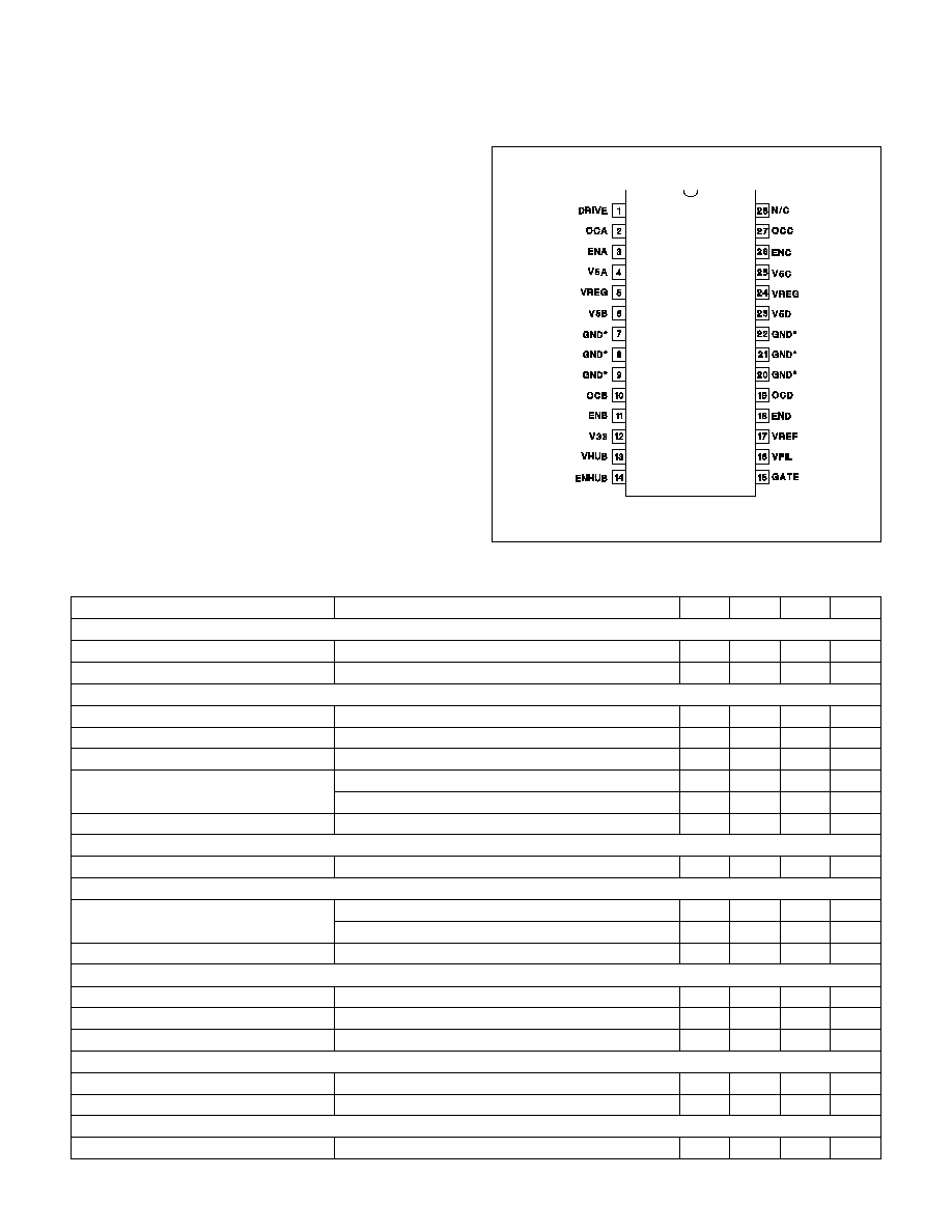
CONNECTION DIAGRAM
SOIC-28 (Top View)
DWP Package
* DWP package pin 28 serves as signal ground; pins 7, 8, 9,
20, 21, 22 serve as heatsink/ground.
3
UCC3831
ENA-D: Separate enables pins for each of the four 5V
supplies.
ENHUB: Enables the 3.3V output V33. Pulling this pin
low disables V33.
GATE: Gate drive for an external NMOS used to regu-
late the 5.5V VREG supply. Minimum available drive is
11V.
GND: All 6 GND pins must be tied to the system
ground. In addition to serving as electrical conductors,
these 6 pins are heat sinks. Refer to the Packaging De-
vice Temperature Management guide in the Packaging
section of the Unitrode Databook.
OCA-D: Open drain overcurrent indicator. OCA-D can
be wire OR'ed by the user to create a single overcurrent
indicator.
V5A-D: 5V regulated output with enable, 500mA (mini-
mum) current limit, and overcurrent indicator.
V33: 3.3V regulator output. Enable when ENHUB is
high. Current limit is 100mA minimum.
VDRIVE: Internal charge pump voltage is brought out
for external decoupling. Nominal voltage is between 11V
and 13V. No external loading permitting. Decouple with
at least 0.001
µ
F capacitor.
VFIL: Bias supply for all four of the 5V regulators. VFIL
voltage must be between 6V and 9V.
VHUB: Supply for the 3.3V USB controller power supply
and bandgap reference.
VREF: Internal 2.5V reference is brought out for exter-
nal decoupling only. Decouple with 0.01
µ
F capacitor.
VREG: Regulated to 5.5V by means of an external
NMOS. 2 pins supply up to a total of 2.5A to the four 5V
bus voltages (V5A, V5B, V5C, V5D).
PIN DESCRIPTIONS
UNITRODE CORPORATION
7 CONTINENTAL BLVD. ∑ MERRIMACK, NH 03054
TEL. (603) 424-2410 ∑ FAX (603) 424-3460
ELECTRICAL CHARACTERISTICS
Unless otherwise specified, T
J
= 0∞C to 125∞C for the UCC3831. VFIL = 6.5V, VHUB
= 5V. T
A
= T
J
.
PARAMETER
TEST CONDITIONS
MIN
TYP
MAX
UNITS
ENHUB Input - Guaranteed High
3
V
Overcurrent Signals
Active Sink Current
I
OCX
=100
m
A
140
500
mV

IMPORTANT NOTICE
Texas Instruments and its subsidiaries (TI) reserve the right to make changes to their products or to discontinue
any product or service without notice, and advise customers to obtain the latest version of relevant information
to verify, before placing orders, that information being relied on is current and complete. All products are sold
subject to the terms and conditions of sale supplied at the time of order acknowledgement, including those
pertaining to warranty, patent infringement, and limitation of liability.
TI warrants performance of its semiconductor products to the specifications applicable at the time of sale in
accordance with TI's standard warranty. Testing and other quality control techniques are utilized to the extent
TI deems necessary to support this warranty. Specific testing of all parameters of each device is not necessarily
performed, except those mandated by government requirements.
CERTAIN APPLICATIONS USING SEMICONDUCTOR PRODUCTS MAY INVOLVE POTENTIAL RISKS OF
DEATH, PERSONAL INJURY, OR SEVERE PROPERTY OR ENVIRONMENTAL DAMAGE ("CRITICAL
APPLICATIONS"). TI SEMICONDUCTOR PRODUCTS ARE NOT DESIGNED, AUTHORIZED, OR
WARRANTED TO BE SUITABLE FOR USE IN LIFE-SUPPORT DEVICES OR SYSTEMS OR OTHER
CRITICAL APPLICATIONS. INCLUSION OF TI PRODUCTS IN SUCH APPLICATIONS IS UNDERSTOOD TO
BE FULLY AT THE CUSTOMER'S RISK.
In order to minimize risks associated with the customer's applications, adequate design and operating
safeguards must be provided by the customer to minimize inherent or procedural hazards.
TI assumes no liability for applications assistance or customer product design. TI does not warrant or represent
that any license, either express or implied, is granted under any patent right, copyright, mask work right, or other
intellectual property right of TI covering or relating to any combination, machine, or process in which such
semiconductor products or services might be or are used. TI's publication of information regarding any third
party's products or services does not constitute TI's approval, warranty or endorsement thereof.
Copyright
©
1999, Texas Instruments Incorporated