 | –≠–ª–µ–∫—Ç—Ä–æ–Ω–Ω—ã–π –∫–æ–º–ø–æ–Ω–µ–Ω—Ç: UCC383-5 | –°–∫–∞—á–∞—Ç—å:  PDF PDF  ZIP ZIP |

SLUS215 - OCTOBER 1998
FEATURES
∑
Precision Positive Series Pass
Voltage Regulation
∑
0.45V Dropout at 3A
∑
50mV Dropout at 10mA
∑
Quiescent Current Under
650µ
A Irrespective of Load
∑
Adjustable (5 Lead) Output
Voltage Version
∑
Fixed (3 Lead) Versions for
3.3V and 5V Outputs
∑
Logic Shutdown Capability
∑
Short Circuit Power Limit of
3%
∑
V
IN
∑
I
SHORT
∑
Low V
OUT
to V
IN
Reverse
Leakage
∑
Thermal Shutdown
DESCRIPTION
The UCC283-3/-5/-ADJ family of positive linear series pass regulators are tailored
for low drop out applications where low quiescent power is important. Fabricated
with a BiCMOS technology ideally suited for low input to output differential applica-
tions, the UCC283-5 will pass 3A while requiring only 0.45V of typical input voltage
headroom (guaranteed 0.6V dropout). These regulators include reverse voltage
sensing that prevents current in the reverse direction. Quiescent current is always
less than 650
µ
A. These devices have been internally compensated in such a man-
ner that the need for a minimum output capacitor has been eliminated.
UCC283-3 and UCC283-5 versions are in 3 lead packages and have preset outputs
at 3.3V and 5.0V respectively. The output voltage is regulated to 1.5% at room tem-
perature. The UCC283-ADJ version, in a 5 lead package, regulates the output volt-
age programmed by an external resistor ratio.
Short circuit current is internally limited. The device responds to a sustained over-
current condition by turning off after a T
ON
delay. The device then stays off for a pe-
riod, T
OFF
, that is 32 times the T
ON
delay. The device then begins pulsing on and off
at the T
ON
/(T
ON
+T
OFF
) duty cycle of 3%. This drastically reduces the power dissipa-
tion during short circuit and means heat sinks need only accommodate normal op-
eration. On the 3 leaded versions of the device T
ON
is fixed at 750
µ
s, on the
adjustable 5 leaded versions an external capacitor sets the on time -- the off time
is always 32 times T
ON
. The external timing control pin, CT, on the five leaded ver-
sions also serves as a shutdown input when pulled low.
Internal power dissipation is further controlled with thermal overload protection cir-
cuitry. Thermal shutdown occurs if the junction temperature exceeds 165∞C. The
chip will remain off until the temperature has dropped 20∞C.
The UCC283 series is specified for operation over the industrial range of
-
40
∞
C to
+85∞C, and the UCC383 series is specified from 0∞C to +70∞C. These devices are
available in 3 and 5 pin TO-220 and TO-263 power packages.
UCC283-3/-5/-ADJ
UCC383-3/-5/-ADJ
Low Dropout 3 Ampere Linear Regulator Family
BLOCK DIAGRAM
UDG-98133
2
UCC283-3/-5/-ADJ
UCC383-3/-5/-ADJ
ABSOLUTE MAXIMUM RATINGS
VIN
. . . . . . . . . . . . . . . . . . . . . . . . . . . . . . . . . . . . . . . . . . . . . . . . . . . . . . . . .
9V
CT . . . . . . . . . . . . . . . . . . . . . . . . . . . . . . . . . . . . . . .
-
0.3 to 3V
ADJ . . . . . . . . . . . . . . . . . . . . . . . . . . . . . . . . . . . . . .
-
0.3 to 9V
Storage Temperature . . . . . . . . . . . . . . . . . . .
-
65∞C to +150
∞
C
Junction Temperature . . . . . . . . . . . . . . . . . . .
-
55
∞
C to +150
∞
C
Lead Temperature (Soldering, 10 sec.) . . . . . . . . . . . . . +300
∞
C
Currents are positive into, negative out of the specified termi-
nal. Consult Packaging Section of Databook for thermal limita-
tions and considerations of packages. All voltages are
referenced to GND.
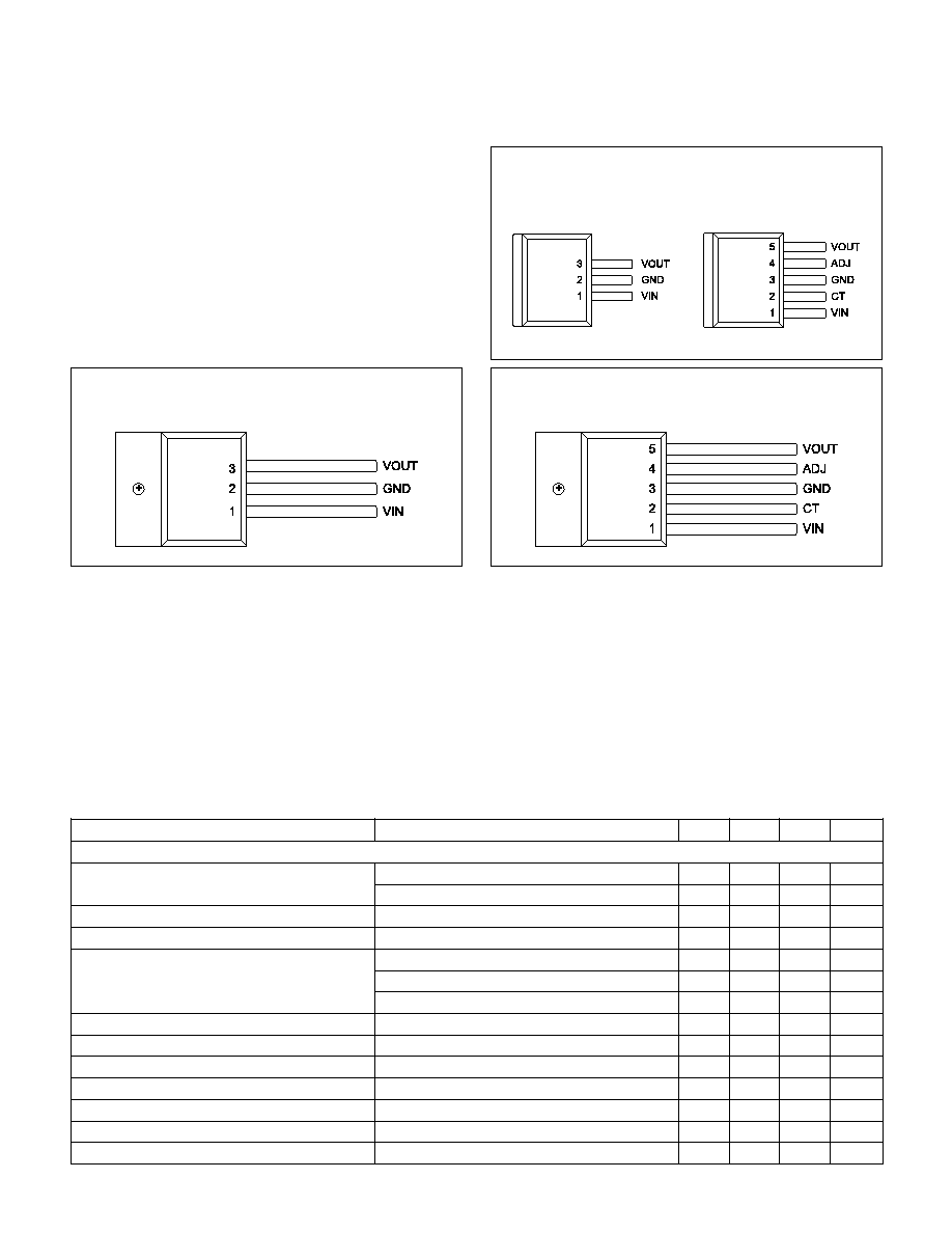
CONNECTION DIAGRAMS
TO-263-3 (Front View)
TD Package
TO-263-5 (Front View)
TD Package
TO-220-3 (Front View)
T Package
TO-220-5 (Front View)
T Package
ELECTRICAL CHARACTERISTICS:
Unless otherwise stated, these specifications hold for T
A
= 0
∞
C to 70
∞
C for the
UCC383-X series,
-
40∞C to +85∞C for the UCC283-X, V
VIN
= V
VOUT
+ 1.5V, I
OUT
= 10mA, C
IN
= 10
µ
F, C
OUT
= 22
µ
F. For the
283-ADJ, V
VIN
= 6.5V, CT = 750pF, T
J
= T
A
.
PARAMETER
TEST CONDITIONS
MIN
TYP
MAX
UNITS
UCC283-5 Fixed 5V, 3A Family
Output Voltage
T
J
= 25
∞
C
4.925
5
5.075
V
Over Temperature
4.875
5.125
V
Line Regulation
V
VIN
= 5.15V to 9V
2
10
mV
Load Regulation
I
OUT
= 10mA to 3A
10
20
mV
Dropout Voltage, V
DROPOUT
= V
VIN
-
V
VOUT
I
OUT
= 3A, VOUT = 4.85V
0.4
0.6
V
I
OUT
= 1.5A, VOUT = 4.85V
0.2
0.45
V
I
OUT
= 10mA, VOUT = 4.85V
50
150
mV
Peak Current Limit
V
VOUT
= 0V
4
5
6.5
A
Overcurrent Threshold
3
4
5.5
A
Current Limit Duty Cycle
V
VOUT
= 0V
3
5
%
Overcurrent Time Out, T
ON
V
VOUT
= 0V
400
750
1400
µ
s
Quiescent Current
No load
400
650
µ
A
Reverse Leakage Current
0V < V
VIN
< V
VOUT,
V
VOUT
5.1V, at V
VOUT
0
75
m
A
UVLO
VIN where VOUT passes current
2.6
2.8
3
V
See Note 1
See Note 1
See Note 1
Note 1: Tab = GND

3
UCC283-3/-5/-ADJ
UCC383-3/-5/-ADJ
ELECTRICAL CHARACTERISTICS:
Unless otherwise stated, these specifications hold for T
A
= 0
∞
C to 70
∞
C for the
UCC383-X series,
-
40∞C to +85∞C for the UCC283-X, V
VIN
= V
VOUT
+ 1.5V, I
OUT
= 10mA, C
IN
= 10
µ
F, C
OUT
= 22
µ
F. For the
283-ADJ, V
VIN
= 6.5V, CT = 750pF, T
J
= T
A
.
PARAMETER
TEST CONDITIONS
MIN
TYP
MAX
UNITS
UCC283-3 Fixed 3.3V, 3A Family
Output Voltage
T
J
= 25
∞
C
3.25
3.3
3.35
V
Over Temperature
3.22
3.38
V
Line Regulation
V
VIN
= 3.45V to 9V
2
7
mV
Load Regulation
I
OUT
= 10mA to 3A
7
15
mV
Dropout Voltage, V
DROPOUT
= V
VIN
-
V
VOUT
I
OUT
= 3A, VOUT = 3.15V
0.5
1
V
I
OUT
= 1.5A, VOUT = 3.15V
0.25
0.6
V
I
OUT
= 10mA, VOUT = 3.15V
50
150
mV
Peak Current Limit
V
VOUT
= 0V
4
5
6.5
A
Overcurrent Threshold
3
4
5.5
A
Current Limit Duty Cycle
V
VOUT
= 0V
3
5
%
Overcurrent Time Out, T
ON
V
VOUT
= 0V
400
750
1400
µ
s
Quiescent Current
No load
400
650
µ
A
Reverse Leakage Current
0V < V
VIN
< V
VOUT,
V
VOUT
3.35V, at V
VOUT
0
75
m
A
UVLO
VIN where VOUT passes current
2.6
2.8
3
V
UCC283-ADJ Adjustable Output, 3A Family
Regulating Voltage at ADJ Pin
T
J
= 25∞C
1.23
1.25
1.27
V
Over Temperature
1.22
1.28
V
Line Regulation, at ADJ Input
V
VIN
= V
VOUT
+ 150mV to 9V
1
3
mV
Load Regulation, at ADJ Input
I
OUT
= 10mA to 3A
2
5
mV
Dropout Voltage, V
DROPOUT
= VIN
-
VOUT
V
VIN
> 4V, I
OUT
= 3A
0.4
0.6
V
V
VIN
> 3V, I
OUT
= 1.5A
0.2
0.45
V
V
VIN
> 3V, I
OUT
= 10mA
50
150
mV
Peak Current Limit
V
VOUT
= 0V, VIN = 6.5V
4
5
6.5
A
Overcurrent Threshold
V
VIN
= 6.5V
3
4
5.5
A
Current Limit Duty Cycle
V
VOUT
= 0V
3
5
%
Overcurrent Time Out, T
ON
V
VOUT
= 0V, CT = 1500pF
750
µ
s
Reverse Leakage Current
0V < V
VIN
< V
VOUT,
V
VOUT
9V, at V
VOUT
0
100
m
A
Bias current at ADJ Input
100
250
nA
Quiescent Current
No load
400
650
µ
A
Shutdown Threshold
At CT Input
0.25
0.45
V
Quiescent Current in Shutdown
V
VIN
= 10V
40
75
µ
A
UVLO
VIN where VOUT passes current
2.6
2.8
3
V

4
UCC283-3/-5/-ADJ
UCC383-3/-5/-ADJ
PIN DESCRIPTIONS
ADJ: Adjust pin for the UCC283-ADJ version only. Feed-
back pin for the linear regulator. Program the output volt-
age with R1 connected from ADJ to GND and R2
connected from VOUT to ADJ. Output voltage is given by:
(
)
VOUT
V R
R
R
=
∑
+
1 25
1
2
1
.
CT: Short circuit timing capacitor and shutdown input for
the UCC283-ADJ version. Pulling CT below 0.25V turns
off the regulator and places it in a low quiescent current
mode. A timing capacitor, C, from CT to GND programs
the duration of the pulsed short circuit on-time. On-time,
T
ON
, is approximately given by:
T
ON
= 500k
∑
C.
GND: Reference ground.
VIN: Input voltage, This pin must be bypassed with a low
ESL/ESR 1
µ
F or larger capacitor to GND. VIN can range
from (VOUT + V
DROPOUT
) to 9V. If VIN is reduced to zero
while VOUT is held high, the reverse leakage from VOUT
to VIN is less than 75
µ
A.
VOUT: Regulated output voltage. A bypass capacitor is
not required at VOUT, but may be desired for good tran-
sient response. The bypass capacitor must not exceed a
maximum value in order to insure the regulator can start.
ORDERING INFORMATION
Temperature
Range
Package
Output Voltage
2: ≠40
∞
C to +85
∞
C
T: TO-220
3: 3.3V
3: 0
∞
C to +70
∞
C
TD: TO-263
5: 5V
ADJ: Adjustable
Table I. Package Information
Overview
The UCC383 family of low dropout linear (LDO) regula-
tors provide a regulated output voltage for applications
with up to 3A of load current. The regulators feature a
low dropout voltage and short circuit protection, making
their use ideal for demanding high current applications
requiring fault protection.
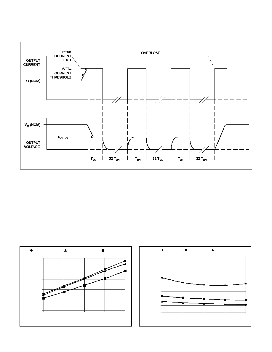
Short Circuit Protection
The UCC383 provides unique short circuit protection
circuitry that reduces power dissipation during a fault.
When an overload situation is detected, the device
enters a pulsed mode of operation at 3% duty cycle
reducing the heat sink requirements during a fault. The
UCC383 has two current thresholds that determine its
behavior during a fault as shown in Figure 1.When the
regulator current exceeds the overcurrent threshold for
a period longer than T
ON
, the UCC383 shuts off for a
period (T
OFF
) which is 32 times T
ON
. During an overload,
the regulator actively limits the maximum current to the
peak current limit value. The peak current limit is
nominally 1 Amp greater than the overcurrent threshold.
The regulator will continue in pulsed mode until the fault
is cleared as illustrated in Figure 1.
Short Circuit Protection
A capacitive load on the regulator's output will appear as
a short circuit during start-up. If the capacitance is too
large, the output voltage will not come into regulation
during the initial T
ON
period and the UCC383 will enter
pulsed mode operation. The peak current limit, T
ON
period, and load characteristics determine the maximum
value of output capacitor that can be charged. For a
constant current load the maximum output capacitance is
given as follows:
(
)
C
I
I
T
V
Farads
OUT
CL
LOAD
ON
OUT
(max)
=
-
∑
(1)
For worst case calculations the minimum values of on
time (T
ON
) and peak current limit (I
CL
) should be used.
The adjustable version allows the T
ON
time to be
adjusted with a capacitor on the CT pin:
T
C Farad
ON ADJ
(
)
,
(
)
=
∑
500 000
m
microseconds
(2)
(
)
T
C
Farads
ON( sec)
,
m
m
=
∑
500 000
For a resistive load (R
LOAD
) the maximum output
capacitor can be estimated from:
C
T
R
n
V
I
R
OUT
ON
LOAD
OUT
CL
LOAD
(max)
(sec)
=
∑
-
∑
Ê
Ë
Á
Á
Á
Á
ˆ
¯
l
1
1
˜
˜
˜
˜
Farads
(3)
APPLICATION INFORMATION
5
UCC283-3/-5/-ADJ
UCC383-3/-5/-ADJ
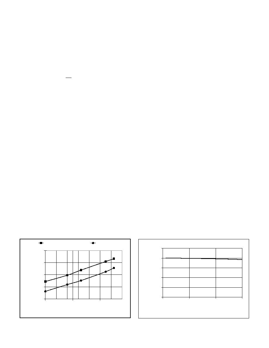
Dropout Performance
Referring to the Block Diagram, the dropout voltage of
the UCC383 is equal to the minimum voltage drop (V
IN
to
V
OUT
) across the N-Channel MOSFET. The dropout
voltage is dependent on operating conditions such as
load current, input and load voltages, as well as
temperature. The UCC383 achieves a low RDS
(ON)
through the use of an internal charge-pump (V
PUMP
) that
drives the MOSFET gate. Figure 2 depicts typical
dropout voltages versus load current for the 3.3V and 5V
versions of the part, as well as the adjustable version
programmed to 3.0V.
Figure 3. depicts the typical dropout performance of the
adjustable version with various output voltages and load
currents.
Operating temperatures also effect the RDS
(ON)
and
dropout voltage of the UCC383. Figure 4. graphs the
typical dropout for the 3.3V and 5V versions with a 3A
load over temperature.
Figure 1. UCC383 Short Circuit Timing
APPLICATION INFORMATION (cont.)
0
0.1
0.2
0.3
0.4
0.5
1
1.5
2
2.5
3
Iout (A)
V
IN
≠V
OU
T
(V)
Vout = 3V
Vout = 3.3V
Vout = 5V
Figure 2. UCC383 Typical Dropout vs. Load Current
0
0.1
0.2
0.3
0.4
0.5
0.6
0.7
0.8
3
3.5
4
4.5
5
V
OUT
(V)
V
IN
≠V
OUT
(V)
Iout = 1A
Iout = 1.5A
Iout = 3A
Figure 3. Typical Dropout Voltage vs. I
OUT
and V
VOUT
6
UCC283-3/-5/-ADJ
UCC383-3/-5/-ADJ
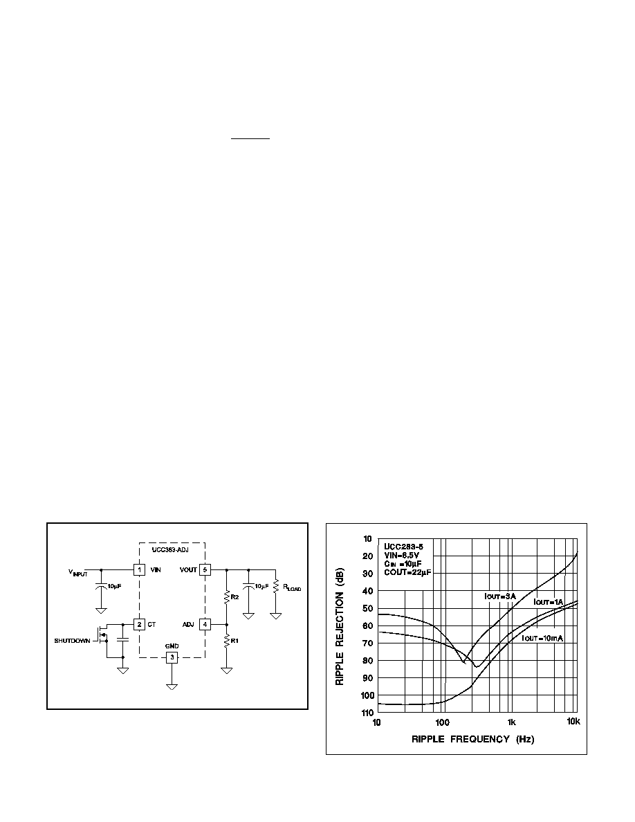
Voltage Programming and Shutdown Feature for
Adjustable Version
A typical application circuit based on the UCC383 adjust-
able version is shown in Figure 5. The output voltage is
externally programmed through a resistive divider at the
ADJ pin.
V
R
R
volts
OUT
=
∑ +
Ê
Ë
Á
ˆ
¯
˜
1 25
1
2
1
.
(4)
The maximum programmed output voltage is constrained
by the 9V absolute rating of the IC (this includes the
charge pump voltage) and its ability to enhance the N-
Channel MOSFET. Unless the load current is below the
3A rating of the device, output voltages above 7V are not
recommended. The minimum output voltage can be pro-
grammed down to 1.25V, however, the input voltage must
always be greater than the UVLO of the part.
The adjustable version includes a shutdown feature, lim-
iting quiescent current to 40uA typical. The UCC383 is
shutdown by pulling the CT pin to below 0.25V. As shown
in Figure 4, a small logic level MOSFET or BJT transistor
in parallel with the timing capacitor can be driven with a
digital signal, putting the device in shutdown. If the CT
pin is not pulled low, the IC will internally pull up on the
pin enabling the regulator. The CT pin should not be
forced high, as this will interfere with the short circuit pro-
tection feature. Selection of the timing capacitor is ex-
plained in
Short Circuit Protection.
The adjustable version can be used in applications re-
quiring remote voltage sensing (i.e. monitoring a voltage
other than or not directly tied to the VOUT pin). This is
possible since the inverting input of the voltage amplifier
(see Block Diagram) is brought out to the ADJ pin.
Thermal Design
The Packing Information section of the data book con-
tains reference material for the thermal ratings of various
packages. The section also includes an excellent article
Thermal Characteristics of Surface Mount Packages, that
is the basis of the following discussion.
Thermal design for the UCC383 includes two modes of
operation, normal and pulsed mode. In normal opera-
tion, the linear regulator and heat sink must dissipate
power equal to the maximum forward voltage drop multi-
plied by the maximum load current. Assuming a constant
current load, the expected heat rise at the regulator's
junction can be calculated as follows:
(
)
T
P
RISE
DISS
jc
ca
( )
q
q
q
=
∑
+
∞C
(5)
Where theta, (
) is thermal resistance and P
DISS
is the
power dissipated. The thermal resistance of both the
TO-220 and TO-263 packages (junction to case) is 3 de-
grees Celsius per Watt. In order to prevent the regulator
from going into thermal shutdown, the case to ambient
theta must keep the junction temperature below 150∞C.
If the LDO is mounted on a 5 square inch pad of 1 ounce
copper, for example, the thermal resistance from junction
to ambient becomes 60 degrees Celsius per Watt. If a
lower thermal resistance is required by the application,
the device heat sinking would need to be improved.
0.2
0.3
0.4
0.5
0.6
-40
10
60
TEMPERATURE (∞C)
V
IN
≠V
OUT
(mv)
Vout = 3.3v
Vout = 5v
Figure 4. Typical dropout voltage vs. case
temperature with a 3A load
0
0.1
0.2
0.3
0.4
0.5
0
1
2
3
LOAD CURRENT (AMPS)
IDD
CURRENT(mAMPS)
Figure 5. Typical application for the 5 pin adjustable
version.
7
UCC283-3/-5/-ADJ
UCC383-3/-5/-ADJ
UNITRODE CORPORATION
7 CONTINENTAL BLVD. ∑ MERRIMACK, NH 03054
TEL. (603) 424-2410
_
FAX (603) 424-3460
When the UCC383 regulator is in pulsed mode due to an
overload or short circuit in the application, the maximum
average power dissipation is calculated as follows:
(
)
P
V
V
I
T
T
Watts
PULSE AVE
IN
OUT
CL
ON
ON
_
≠
=
∑
∑
∑
33
(6)
As seen in equation 6, the average power during a fault
is reduced dramatically by the duty cycle, allowing the
heat sink to be sized for normal operation. Although the
peak power in the regulator during the T
ON
period can be
significant, the thermal mass of the package will gener-
ally keep the junction temperature from rising unless the
T
ON
period is increased to tens of milliseconds.
Ripple Rejection
Even though the UCC383 family of linear regulators are
not optimized for fast transient applications (Refer to
UC182 Fast LDO Linear Regulator), they do offer
significant power supply rejection at lower frequencies.
Figure 6 depicts ripple rejection performance in a typical
application. The performance can be improved with
additional filtering.
Figure 7. Ripple rejection vs. frequency.
UDG-94093
Figure 6. Typical supply current vs. load current.

IMPORTANT NOTICE
Texas Instruments and its subsidiaries (TI) reserve the right to make changes to their products or to discontinue
any product or service without notice, and advise customers to obtain the latest version of relevant information
to verify, before placing orders, that information being relied on is current and complete. All products are sold
subject to the terms and conditions of sale supplied at the time of order acknowledgement, including those
pertaining to warranty, patent infringement, and limitation of liability.
TI warrants performance of its semiconductor products to the specifications applicable at the time of sale in
accordance with TI's standard warranty. Testing and other quality control techniques are utilized to the extent
TI deems necessary to support this warranty. Specific testing of all parameters of each device is not necessarily
performed, except those mandated by government requirements.
CERTAIN APPLICATIONS USING SEMICONDUCTOR PRODUCTS MAY INVOLVE POTENTIAL RISKS OF
DEATH, PERSONAL INJURY, OR SEVERE PROPERTY OR ENVIRONMENTAL DAMAGE ("CRITICAL
APPLICATIONS"). TI SEMICONDUCTOR PRODUCTS ARE NOT DESIGNED, AUTHORIZED, OR
WARRANTED TO BE SUITABLE FOR USE IN LIFE-SUPPORT DEVICES OR SYSTEMS OR OTHER
CRITICAL APPLICATIONS. INCLUSION OF TI PRODUCTS IN SUCH APPLICATIONS IS UNDERSTOOD TO
BE FULLY AT THE CUSTOMER'S RISK.
In order to minimize risks associated with the customer's applications, adequate design and operating
safeguards must be provided by the customer to minimize inherent or procedural hazards.
TI assumes no liability for applications assistance or customer product design. TI does not warrant or represent
that any license, either express or implied, is granted under any patent right, copyright, mask work right, or other
intellectual property right of TI covering or relating to any combination, machine, or process in which such
semiconductor products or services might be or are used. TI's publication of information regarding any third
party's products or services does not constitute TI's approval, warranty or endorsement thereof.
Copyright
©
1999, Texas Instruments Incorporated