10/96
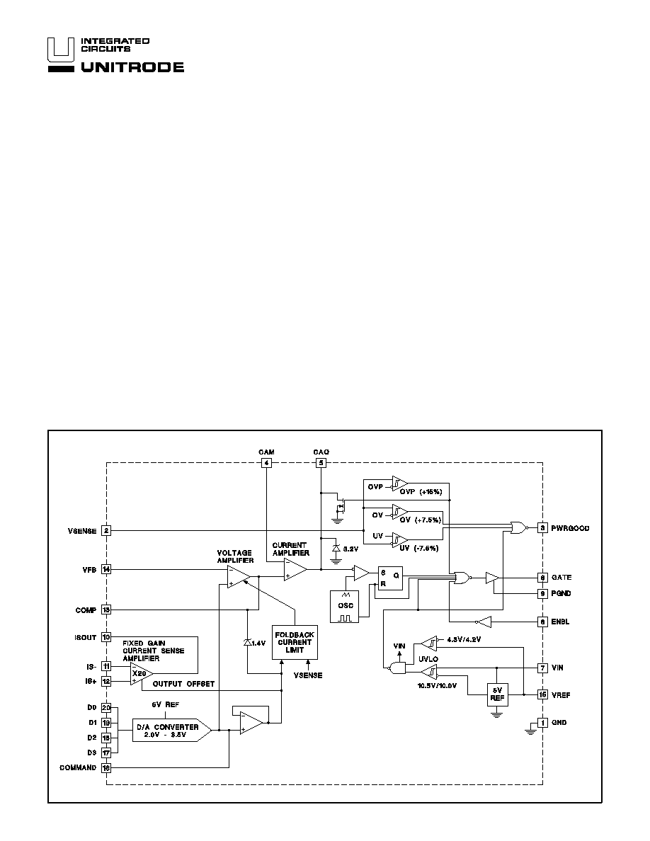
BLOCK DIAGRAM
∑
Combined DAC/Voltage
Monitor and PWM Functions
∑
4-Bit Digital-to-Analog
Converter (DAC)
∑
1.0% DAC/Reference
∑
Low Offset X20 Current Sense
Amplifier
∑
100kHz, 200kHz, 400kHz
Oscillator Frequency Options
∑
Foldback Current Limiting
∑
Overvoltage and Undervoltage
Fault Windows
∑
Undervoltage Lockout
∑
2
Totem Pole Output
∑
Chip Disable Function
PentiumÆ Pro Controller
FEATURES
DESCRIPTION
UDG-96106-1
UCC2880-4/-5/-6
UCC3880-4/-5/-6
PRELIMINARY
The UCC3880-4/-5/-6 combines high precision reference and voltage monitor-
ing circuitry with average current mode PWM controller circuitry to power Intel
Pentium Pro and other high-end microprocessors with a minimum of external
components. The UCC3880-x converts 5VDC to an adjustable output, ranging
from 2.0VDC to 3.5VDC in 100mV steps with 1% DC system accuracy.
The chip includes a precision 5V reference which is capable of sourcing cur-
rent to an external load. The output voltage of the DAC is derived from this
reference, and is programmed directly by Intel's VID pins (Table 1).
The accuracy of the DAC/reference combination is 1.0%. The overvoltage and
undervoltage comparators monitor the system output voltage and indicate
when it rises above or falls below its programmed value by more than 7.5%. A
second overvoltage protection comparator pulls the current amplifier output
voltage low to force zero duty cycle when the system output voltage exceeds
its designed value by more than 15%. This comparator also terminates the cy-
cle. Undervoltage lockout circuitry assures the correct logic states at the out-
puts during powerup and powerdown. Grounding the ENABLE pin forces the
GATE output low.
(continued)
UCC2880-4/-5/-6
UCC3880-4/-5/-6
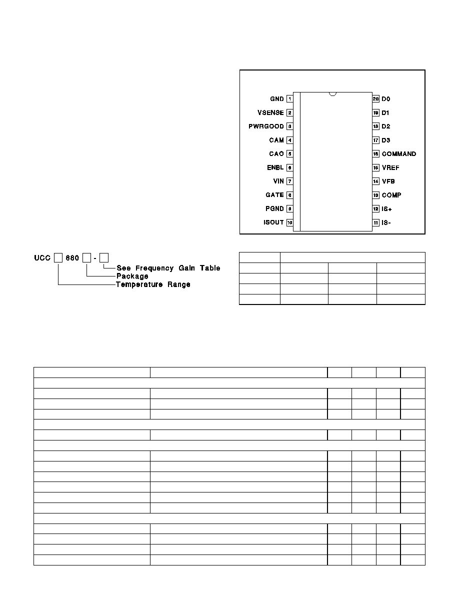
CONNECTION DIAGRAM
SOIC-20 (Top View)
DW Package
ELECTRICAL CHARACTERISTICS:
Unless otherwise specified, VIN = 12V, VSENSE = 3.5V, V
ENBL
= 5V, VD0 = VD1 = VD2
= VD3 = 0V, 0∞C < T
A
< 70∞C, T
A
= T
J
.
PARAMETER
TEST CONDITIONS
MIN
TYP
MAX
UNITS
Undervoltage Lockout
VIN UVLO Turn-on Threshold
10.5
10.8
V
VIN UVLO Turn-off Threshold
9.5
10
V
UVLO Threshold Hysteresis
500
mV
Supply Current
l
IN
3.5
mA
DAC/Reference
COMMAND Voltage Accuracy
10.8V < VIN < 13.2V, I
VREF
= 0mA
≠1
1
%
D0-D3 Voltage High
DX Pin Floating
5
V
D0-D3 Input Bias Current
DX Pin Tied to GND
≠70
≠20
µ
A
VREF Output Voltage
4.975
5
5.025
V
VREF Load Regulation
I
VREF
= 0mA to 5mA
≠10
0
mV
VREF Sourcing Current
VREF = 0V
10
mA
OVP Comparator
Trip Point
% Over COMMAND Voltage
10
15
20
%
Hysteresis
20
30
mV
VSENSE Input Bias Current
OV, OVP, UV Combined
≠0.1
µ
A
Propagation Delay
1
µ
s
The voltage and current amplifiers have a 4MHz gain
bandwidth product to satisfy high performance system re-
quirements. The internal current sense amplifier permits
the use of a low value current sense resistor, minimizing
power loss. The oscillator frequency is fixed internally at
100kHz, 200kHz, or 400kHz, depending upon the option
selected. The foldback circuit reduces the converter short
circuit current limit to 50% of its nominal value when the
converter is short circuited. The gate driver is a 2
totem
pole output stage capable of driving an external MOSFET.
This device is available in 20-pin dual in-line and surface
mount packages. The UCC2880-x is specified for opera-
tion from ≠25∞C to 85∞C, and the UCC3880-x is specified
for operation from 0∞C to 70∞C.
PentiumÆ Pro is a registered trademark of Intel Corpora-
tion.
DESCRIPTION (cont.)
Frequency
100kHz
200kHz
400kHz
UCC3880-4
X
UCC3880-5
X
UCC3880-6
X
Frequency Gain Table
ORDERING INFORMATION
Consult factory for temperature range or package options
not shown.
2

ELECTRICAL CHARACTERISTICS (cont.):
Unless otherwise specified, VIN = 12V, VSENSE = 3.5V, V
ENBL
= 5V, VD0 =
VD1 = VD2 = VD3 = 0V, 0∞C < T
A
< 70∞C, T
A
= T
J
.
PARAMETER
TEST CONDITIONS
MIN
TYP
MAX
UNITS
OV Comparator
Trip Point
% Over COMMAND Voltage (Note 1)
7.6
10
%
Return Point
% Over COMMAND Voltage (Note 1)
5
7.4
%
Hysteresis
20
30
mV
PWRGOOD Equivalent Resistance VSENSE = 2.0V
470
Propagation Delay
1
µ
s
UV Comparator
Trip Point
% Over COMMAND Voltage (Note 1)
≠10
≠7.6
%
Return Point
% Over COMMAND Voltage (Note 1)
≠7.4
≠5
%
Hysteresis
20
30
mV
Propagation Delay
1
µ
s
Enable Pin
Pull-up Current
V
ENBL
= 2.5V
≠50
≠20
µ
A
Voltage Error Amplifier
Input Offset Voltage
V
COMP
= 3.5V
0.0
mV
Input Bias Current
V
CM
= 3.0V
≠0.02
0
µ
A
Open Loop Gain
1V < V
COMP
< 4V
90
dB
Common Mode Rejection Ratio
2V < V
COMP
< 3.5V
90
dB
Power Supply Rejection Ratio
10.8V < VIN < 15V
85
dB
Output Sourcing Current
V
VFB
= 2V, V
COMMAND
= V
COMP
= 2.5V
≠0.5
mA
Output Sinking Current
V
VFB
= 3V, V
COMMAND
= V
COMP
= 2.5V
2.0
mA
Gain Bandwidth Product
F = 100kHz
3
MHz
Current Sense Amplifier
Gain
20
V/V
Input Resistance
5
k
Common Mode Rejection Ratio
0V < V
CM
< 4.5V
60
dB
Power Supply Rejection Ratio
10.8V < VIN < 15V
80
dB
Output Sourcing Current
V
IS
≠ = 2V, V
ISOUT
= V
IS
+ = 2.5V
≠0.5
mA
Output Sinking Current
V
IS≠
= 3V, V
ISOUT
= V
IS+
= 2.5V
6.0
mA
≠3dB Frequency
At GAIN = 20
1.75
MHz
Current Amplifier
Input Offset Voltage
V
CM
= 3.0V
10
mV
Input Bias Current
V
CM
= 3.0V
0.15
µ
A
Open Loop Gain
1V < V
CAO
< 3V
90
dB
Output Voltage High
V
COMP
= 3V, V
CAM
= 2.5V
3.2
V
Common Mode Rejection Ratio
1.5V < V
CM
< 4.9V
80
dB
Power Supply Rejection Ratio
10.8V < VIN < 15V
80
dB
Output Sourcing Current
V
CAM
= 2V, V
CAO
= V
COMP
= 2.5V
≠0.5
mA
Output Sinking Current
V
CAM
= 3V, V
CAO
= V
COMP
= 2.5V
2.0
mA
Gain Bandwidth Product
F = 100kHz
3.5
MHz
UCC2880-4/-5/-6
UCC3880-4/-5/-6
3
UCC2880-4/-5/-6
UCC3880-4/-5/-6
PIN DESCRIPTIONS (cont.)
CAM (Current Amplifier Inverting Input): The average
load current feedback from ISOUT is applied through a
resistor to this pin. The current loop compensation net-
work is also connected to this pin (see CAO below).
CAO (Current Amplifier Output): The current loop com-
pensation network is connected between this pin and
CAM. The voltage on this pin is the input to the PWM
comparator and regulates the output voltage of the sys-
tem. The GATE output is disabled (held low) unless the
voltage on this pin exceeds 1V, allowing the PWM to
force zero duty cycle when necessary. The PWM forces
maximum duty cycle when the voltage on CAO exceeds
the oscillator peak voltage (3V). A 3.2V clamp circuit pre-
vents the CAO voltage from rising excessively past the
oscillator peak voltage for excellent transient response.
COMMAND (Digital-to-Analog Converter Output Volt-
age): This pin is the output of the 4-bit digital-to-analog
converter (DAC) and the noninverting input of the voltage
amplifier. The voltage on this pin sets the switching regu-
lator output voltage. Setting all input control codes low
produces 3.5V at COMMAND; setting all codes high pro-
duces 2.0V at COMMAND. The DAC LSB step size (i.e.
resolution) is 100mV (See Table 1). The COMMAND
source impedance is typically 1.2k
and must therefore
drive only high impedance inputs if accuracy is to be
maintained. Bypass COMMAND with a 0.01
µ
F, low ESR,
low ESL capacitor for best circuit noise immunity.
COMP (Voltage Amplifier Output): The system voltage
compensation network is applied between COMP and
VFB.
D0 - D3 (DAC Digital Input Control Codes): These are
the DAC digital input control codes, with D0 representing
the least significant bit (LSB) and D3, the most significant
bit (MSB). A bit is set low by being connected to GND. A
ELECTRICAL CHARACTERISTICS (cont.):
Unless otherwise specified, VIN = 12V, VSENSE = 3.5V, V
ENBL
= 5V, VD0 =
VD1 = VD2 = VD3 = 0V, 0∞C < T
A
< 70∞C, T
A
= T
J
.
PARAMETER
TEST CONDITIONS
MIN
TYP
MAX
UNITS
Oscillator
Frequency (-4)
85
100
115
kHz
Frequency (-5)
200
kHz
Frequency (-6)
400
kHz
Frequency Change With Voltage
10.8V < VIN < 15V
1
%
Output Section
Maximum Duty Cycle
90
95
99
%
Output Low Voltage
I
GATE
= ≠100mA
0.20
V
Output High Voltage
I
GATE
= 100mA
11.8
V
Rise Time
C
GATE
= 3.3nF
20
80
ns
Fall Time
C
GATE
= 3.3nF
15
80
ns
Output Impedance
I
GATE
= 100mA
2
I
GATE
= ≠100mA
2
Foldback Current Limit
Clamp Level
Measured at Voltage EA Output;
V
SENSE
= V
COMMAND
= 3V
4.4
V
V
COMMAND
= 3V, V
SENSE
= 0
3.7
V
Note 1: This percentage is measured with respect to the ideal COMMAND voltage programmed by the D0 - D3 pins.
Decimal
Code
D3
D2
D1
D0
COMMAND
Voltage
15
1
1
1
1
2.0
14
1
1
1
0
2.1
13
1
1
0
1
2.2
12
1
1
0
0
2.3
11
1
0
1
1
2.4
10
1
0
1
0
2.5
9
1
0
0
1
2.6
8
1
0
0
0
2.7
7
0
1
1
1
2.8
6
0
1
1
0
2.9
5
0
1
0
1
3.0
4
0
1
0
0
3.1
3
0
0
1
1
3.2
2
0
0
1
0
3.3
1
0
0
0
1
3.4
0
0
0
0
0
3.5
Table 1. Programming the COMMAND Voltage
4

UCC2880-4/-5/-6
UCC3880-4/-5/-6
PIN DESCRIPTIONS (cont.)
bit is set high by floating it, or connecting it to a 5V
source. Each control pin is pulled up to approximately 5V
by an internal 70
µ
A current source.
ENBL (Chip Enable Pin): This input is used to disable
the GATE and PWRGOOD outputs. Grounding this pin
causes the GATE output to be held low; floating the pin or
pulling it up to 5V ensures normal operation. ENBL is
pulled up to 5V internally.
GATE (PWM Output, MOSFET Driver): This output pro-
vides a 2
totem pole driver. Use a series resistor of at
least 5
between this pin and the gate of the external
MOSFET to prevent excessive overshoot.
GND (Signal Ground): All voltages are measured with
respect to GND. Bypass capacitors on the VCC and
VREF pins should be connected directly to the ground
plane near the GND pin.
IS≠ (Current Sense Amplifier Inverting Input): This pin
is the inverting input to the current sense amplifier and is
connected to the low side of the average current sense
resistor.
IS+ (Current Sense Amplifier Noninverting Input):
This pin is the noninverting input to the current sense am-
plifier and is connected to the high side of the average
current sense resistor.
ISOUT (Current Sense Amplifier Output): This pin is
the output of the current sense amplifier. The voltage on
this pin is (COMMAND + G
CSA
∑
I
∑
R
SENSE
), where
COMMAND is the voltage on the COMMAND pin, G
CSA
is the fixed gain of the current sense amplifier, equal to
20, I
is the current through the sense resistor, and
R
SENSE
is the value of the average current sensing resis-
tor.
PGND (Power Ground): This pin provides a dedicated
ground for the output gate driver. The GND and PGND
pins should be connected externally using a short printed
circuit board trace close to the IC. Decouple VIN to
PGND with a low ESR capacitor
0.10
µ
F.
PWRGOOD (Undervoltage/Lower Overvoltage Out-
put): This pin is an open drain output which is driven low
to reset the microprocessor when VSENSE rises above
or falls below its nominal value by 7.5%. The on resis-
tance of the open drain switch will be no higher than
470
. The OV and UV comparators' hysteresis is fixed at
20mV independent of the COMMAND voltage.
VIN (Positive Supply Voltage): This pin supplies power
to the chip. Connect VIN to a stable voltage source of at
least 10.8V. The GATE and PWRGOOD outputs will be
held low until VCC exceeds the upper undervoltage lock-
out threshold. This pin should be bypassed directly to the
GND pin.
VFB (Voltage Amplifier Inverting Input): This input is
connected to COMP through a feedback network and to
the power supply output through a resistor or a divider
network.
VREF (Voltage Reference Output): This pin provides an
accurate 5V reference and is internally short circuit cur-
rent limited. VREF powers the D/A converter and also
provides a threshold voltage for the UVLO comparator.
For best reference stability, bypass VREF directly to GND
with a low ESR, low ESL capacitor of at least 0.01
µ
F.
VSENSE (Output Voltage Sensing Input): This pin is
connected to the system output voltage through a low
pass filter. When the voltage on VSENSE rises above or
falls below the COMMAND voltage by 7.5%, the
PWRGOOD output is driven low to reset the microproc-
essor. When the voltage on VSENSE rises above the
COMMAND voltage by 15%, the OVP comparator pulls
the current amplifier output voltage below the oscillator
valley voltage to force zero duty cycle at the GATE out-
put. This pin is also used by the foldback current limiting
circuitry.
Current Limit
The short circuit current limit, I
SC
, is set according to:
I
SC
=
1.4V
R
SENSE
∑
G
CSA
where R
SENSE
is the average current sense resistor and
G
CSA
is the current sense amplifier gain, where G
CSA
equals 20. Example: Choose R
SENSE
to set the short cir-
cuit current limit at 16A using the UCC3880-5
R
SENSE
=
1.4V
16A
∑
20
=
4.4m
A lower resistance value may be needed if the AC ripple
current in the inductor is more than 20% of the full load
current.
Related Publications
U-156 and U-157 are Unitrode Application Notes describ-
ing the operation of the UC3886 and the UC3886/
UC3910 together in a PentiumÆ Pro application.
APPLICATION INFORMATION
5
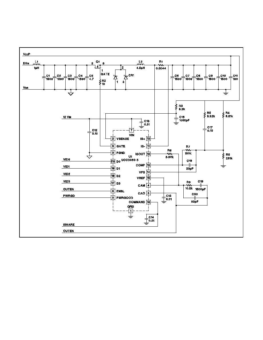
UCC3880 Configured for Powering the PentiumÆ Pro
TYPICAL APPLICATION
The UCC3880-x is ideal for converting the 5.0V system
bus into the required PentiumÆ Pro bus voltage.
UDG-96224
UCC2880-4/-5/-6
UCC3880-4/-5/-6
6

UNITRODE INTEGRATED CIRCUITS
7 CONTINENTAL BLVD.
∑
MERRIMACK, NH 03054
TEL. (603) 424-2410
∑
FAX (603) 424-3460
PentiumÆ Pro is a registered trademark of Intel Corporation.
UCC2880-4/-5/-6
UCC3880-4/-5/-6
REF.
DESCRIPTION
PACKAGE
U1
Unitrode UCC3830DWP-5 DAC/PWM
SOIC-20 Wide
C1
Sanyo 6MV1500GX, 1500
µ
F, 6.3V, Aluminum Electrolytic
10x20mm Radial Can
C2
Sanyo 6MV1500GX, 1500
µ
F, 6.3V, Aluminum Electrolytic
10x20mm Radial Can
C3
Sanyo 6MV1500GX, 1500
µ
F, 6.3V, Aluminum Electrolytic
10x20mm Radial Can
C4
Sanyo 6MV1500GX, 1500
µ
F, 6.3V, Aluminum Electrolytic
10x20mm Radial Can
C5
Sprague/Vishay 595D475X0016A2B, 4.7
µ
F 16V Tantalum
SPRAGUE Size A
C6
Sanyo 6MV1500GX, 1500
µ
F, 6.3V, Aluminum Electrolytic
10x20mm Radial Can
C7
Sanyo 6MV1500GX, 1500
µ
F, 6.3V, Aluminum Electrolytic
10x20mm Radial Can
C8
Sanyo 6MV1500GX, 1500
µ
F, 6.3V, Aluminum Electrolytic
10x20mm Radial Can
C9
Sanyo 6MV1500GX, 1500
µ
F, 6.3V, Aluminum Electrolytic
10x20mm Radial Can
C10
Sanyo 6MV1500GX, 1500
µ
F, 6.3V, Aluminum Electrolytic
10x20mm Radial Can
C11
Sprague 593D107X9010D2, 100
µ
F, 6.3V Tantalum
EIA Size D SMD
C12
0.10
µ
F Ceramic
1206 SMD
C13
0.01
µ
F Ceramic
0603 SMD
C14
0.01
µ
F Ceramic
0603 SMD
C15
0.01
µ
F Ceramic
0603 SMD
C16
1000pF Ceramic
0603 SMD
C17
0.10
µ
F Ceramic
1206 SMD
C18
33pF NPO Ceramic
0603 SMD
C19
1500pF Ceramic
0603 SMD
C20
82pF NPO Ceramic
0603 SMD
C21
0.10
µ
F Ceramic
1206 SMD
C22
0.10
µ
F Ceramic
1206 SMD
CR1
International Rectifier 32CTQ030 30V, 30A Schottky Diode
TO-220AB
L1
Micrometals T50-52B, 10 Turns #16AWG, 4.5
µ
H
Toroid
Q1
International Rectifier IRL3103, 30V, 56A
TO-220AB
R1
Dale/Vishay WSR-2 0.005
1%
SMD Power Package
R2
10
, 5%, 1/16 Watt
0603 SMD
R3
8.2k
, 5%, 1/16 Watt
0603 SMD
R4
6.81k
, 1%, 1/16 Watt
0603 SMD
R5
3.92k
, 1%, 1/16 Watt
0603 SMD
R6
261k
, 1%, 1/16 Watt
0603 SMD
R7
100k
, 1%, 1/16 Watt
0603 SMD
R8
3.92k
, 1%, 1/16 Watt
0603 SMD
R9
10.5k
, 1%, 1/16 Watt
0603 SMD
Q1-HS
AAVID 576802 TO-220 Heat Sink
TO-220AB
CR1-HS
AAVID 577002 TO-220 Heat Sink
TO-220AB
PARTS LIST
7

IMPORTANT NOTICE
Texas Instruments and its subsidiaries (TI) reserve the right to make changes to their products or to discontinue
any product or service without notice, and advise customers to obtain the latest version of relevant information
to verify, before placing orders, that information being relied on is current and complete. All products are sold
subject to the terms and conditions of sale supplied at the time of order acknowledgement, including those
pertaining to warranty, patent infringement, and limitation of liability.
TI warrants performance of its semiconductor products to the specifications applicable at the time of sale in
accordance with TI's standard warranty. Testing and other quality control techniques are utilized to the extent
TI deems necessary to support this warranty. Specific testing of all parameters of each device is not necessarily
performed, except those mandated by government requirements.
CERTAIN APPLICATIONS USING SEMICONDUCTOR PRODUCTS MAY INVOLVE POTENTIAL RISKS OF
DEATH, PERSONAL INJURY, OR SEVERE PROPERTY OR ENVIRONMENTAL DAMAGE ("CRITICAL
APPLICATIONS"). TI SEMICONDUCTOR PRODUCTS ARE NOT DESIGNED, AUTHORIZED, OR
WARRANTED TO BE SUITABLE FOR USE IN LIFE-SUPPORT DEVICES OR SYSTEMS OR OTHER
CRITICAL APPLICATIONS. INCLUSION OF TI PRODUCTS IN SUCH APPLICATIONS IS UNDERSTOOD TO
BE FULLY AT THE CUSTOMER'S RISK.
In order to minimize risks associated with the customer's applications, adequate design and operating
safeguards must be provided by the customer to minimize inherent or procedural hazards.
TI assumes no liability for applications assistance or customer product design. TI does not warrant or represent
that any license, either express or implied, is granted under any patent right, copyright, mask work right, or other
intellectual property right of TI covering or relating to any combination, machine, or process in which such
semiconductor products or services might be or are used. TI's publication of information regarding any third
party's products or services does not constitute TI's approval, warranty or endorsement thereof.
Copyright
©
1999, Texas Instruments Incorporated