UCC391
ADVANCE INFORMATION
DESCRIPTION
The UCC391 provides an accurate reference, programmable by a 5-bit
DAC, in a tiny 8 pin package. Using few external components, the UCC391
converts 5V to an adjustable output ranging from 3.5VDC to 2.1VDC in
100mV steps and 2.05VDC to 1.3VDC in 50mV steps with 1% DC system
accuracy.
This device is available in and 8 pin surface mount (150mm SOIC) and
TSSOP packages and is specified for operation from 0∞C to 70∞C.
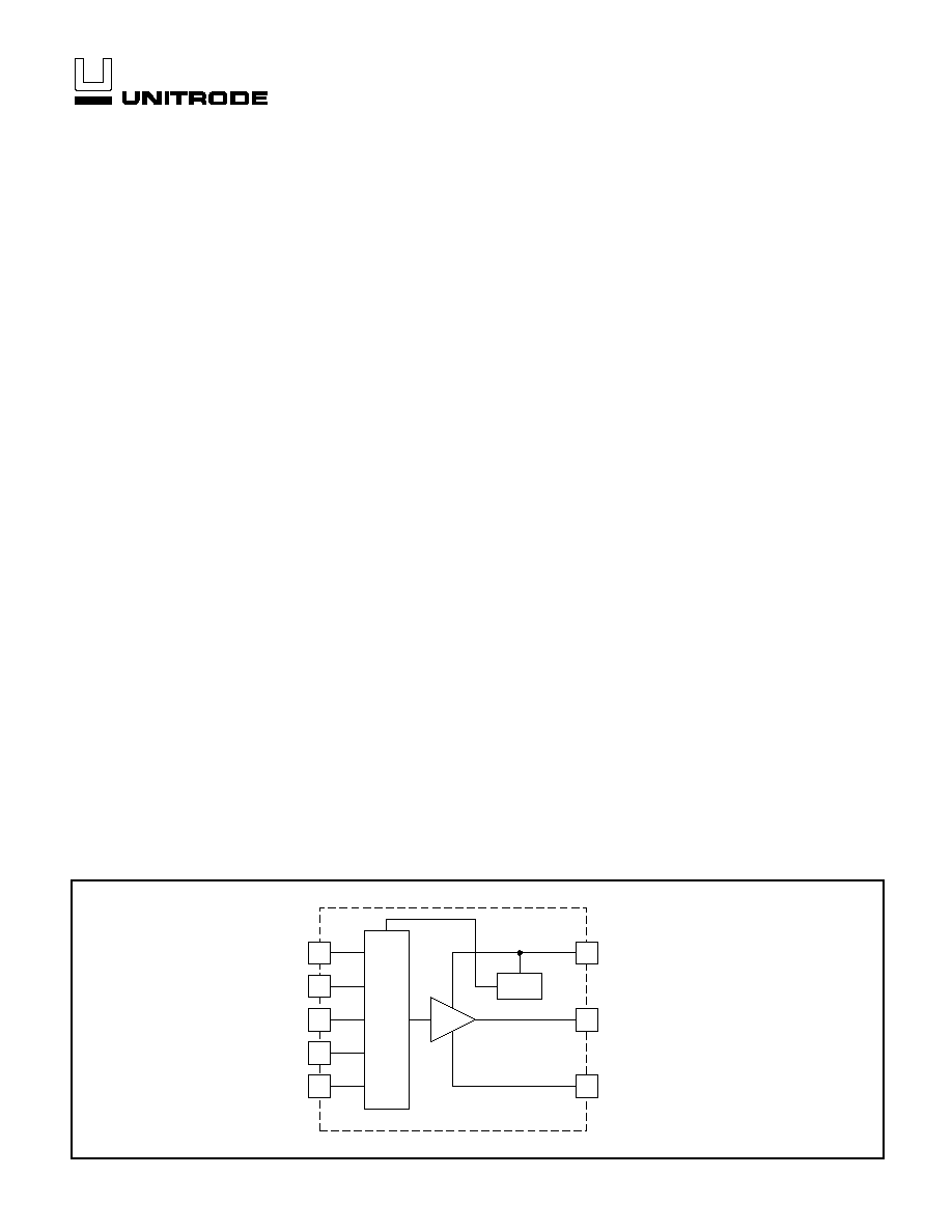
5-Bit Programmable Output BiCMOS Precision Voltage Reference
FEATURES
∑ 5 - Bit Digital-to-Analog Converter
(DAC) supports Intel Pentium II
Microprocessor VID Codes
∑ Compatible with 5V Systems
∑ 1% Output Voltage Accuracy
Guaranteed
SLUS437 - NOVEMBER 1998
7
8
4
1
2
5
3
D4
D3
D2
D1
D0
6
VCC
COMMAND
GND
DAC
VREF
BLOCK DIAGRAM
UDG-98200
2
UCC391
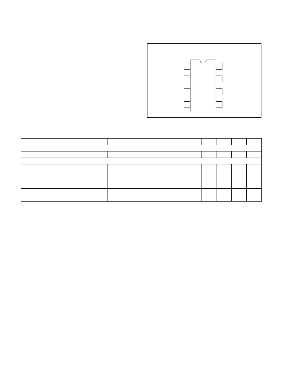
MSOP-8, TSSOP-8 (TOP VIEW)
P, PW Packages
ABSOLUTE MAXIMUM RATINGS
Supply Voltage V
CC
. . . . . . . . . . . . . . . . . . . . . . . . . . . . . . . . 8V
Input Voltage, D0, D1, D2, D3, D4 . . . . . . . . . . . . . . . . . . . . 8V
Currents are positive into, negative out of the specified termi-
nal. Consult Packaging Section of Databook for thermal limita-
tions and considerations of packages. All voltages are
referenced to GND.
GND
D4
D3
COMMAND
D1
D2
D0
VCC
1
2
3
4
8
7
6
5
CONNECTION DIAGRAMS
ELECTRICAL CHARACTERISTICS:
Unless otherwise specified these specifications hold for T
A
= 0∞C to 70∞C for the
UCC391, T
A
= T
J
. V
CC
= 5V.
PARAMETER
TEST CONDITIONS
MIN
TYP
MAX
UNITS
Supply Current Section
Supply Current, On
V
CC
= 5V
1.8
mA
DAC Reference Section
COMMAND Voltage Accuracy
4.5V < V
IN
< 5.5V, measured on COMMAND, 0∞C
< T
A
< 70∞C (Note 1)
≠1.00
1.00
%
D0 ≠ D4 Voltage High
4.5
5
5.5
V
D0 ≠ D4 Voltage Threshold
2.5
V
D0 ≠ D4 Input Bias Current
V(D4, D3, D2, D1, D0) < 0.5V
≠90
≠20
µ
A
Output Current (Maximum Load)
I
OUT
(V
COMMAND
)
0
150
µ
A
Note 1: Reference and output amplifier offsets are trimmed out before packaging.
GND: (Ground) All voltages measured with respect to
ground. VCC should be bypassed directly to GND with a
0.1
µF or larger ceramic capacitor.
VCC: (Positive supply voltage) This pin is normally con-
nected to a 5V
± 10% system voltage. Bypass VCC di-
rectly to GND with a 0.1
µF (minimum) ceramic capacitor.
COMMAND: This pin is the output of the IC. It is con-
trolled by the 5-bit input word (D0:D4). This output will
have a
±1% system accuracy over temperature, process,
and input voltage.
D0, D1, D2, D3, D4: These are the digital input control
codes for the DAC. The DAC is comprised of two ranges
set by D4, with D0 representing the least significant bit
(LSB) and D3, the most significant bit (MSB). A bit is set
low by being connected to GND; a bit is set high by float-
ing the pin. Each control pin is pulled up to approximately
5V by an internal pull-up. If all ones are commanded on
the DAC inputs (no CPU command), the output will be
disabled.
PIN DESCRIPTIONS