 | –≠–ª–µ–∫—Ç—Ä–æ–Ω–Ω—ã–π –∫–æ–º–ø–æ–Ω–µ–Ω—Ç: UCC3911-3 | –°–∫–∞—á–∞—Ç—å:  PDF PDF  ZIP ZIP |

UCC3911-1, UCC3911-2
UCC3911-3, UCC3911-4
SLUS429B≠ FEBRUARY 2000 ≠ REVISED NOVEMBER 2002
LITHIUM ION AND LITHIUM POLYMER
BATTERY PROTECTOR
1
www.ti.com
FEATURES
D
Protects Sensitive Lithium-Ion and
Lithium-Polymer Cells from Overcharging
and Overdischarging
D
Used for Two-Cell Battery Packs
D
No External FETs Required
D
Provides Protection Against Battery Pack
Output Short Circuit
D
Extremely Low Power Drain on Batteries of
About 20
µ
A
D
Low Internal FET Switch Voltage Drop
D
User Controllable Delay for Tripping Short
Circuit Current Protector
D
3-A Current Capacity
APPLICATIONS
D
PDA, Camcorder, Digital Camera, Private
Mobile Radio
SIMPLIFIED APPLICATION DIAGRAM
DESCRIPTION
The UCC3911 is a two-cell lithium-ion (Li-Ion) and
lithium-polymer (Li-Pol) battery pack protector
device that incorporates an on-chip series FET
switch thus reducing manufacturing costs and
increasing reliability. The device's primary
function is to protect both Li-Ion and Li-Pol cells in
a two-cell battery pack from being either
overcharged (overvoltage) or overdischarged
(undervoltage). It employs a precision bandgap
voltage reference that is used to detect when
either cell is approaching an overvoltage or
undervoltage state. When on-board logic detects
either condition, the series FET switch opens to
protect the cells.
A negative feedback loop controls the FET switch
when the battery pack is in either the overvoltage
or undervoltage state. In the overvoltage state the
action of the feedback loop is to allow only
discharge current to pass through the FET switch.
In the undervoltage state, only charging current is
allowed to flow. The operational amplifier that
drives the loop is powered only when in one of
these two states. In the undervoltage state the
chip enters sleep mode until it senses that the
pack is being charged.
The FET switch is driven by a charge pump when
the battery pack is in a normally charged state to
achieve the lowest possible R
DS(on)
. In this state
the negative feedback loop's operational amplifier
is powered down to conserve battery power. Short
circuit protection for the battery pack is provided
and has a nominal delay of 100
µ
s before tripping.
An external capacitor may be connected between
CDLY and B0 to increase this delay time to allow
longer overcurrent transients.
A chip enable (CE) pin is provided that when held
low, inhibits normal operation of the device to
facilitate assembly of the battery pack.
PRODUCTION DATA information is current as of publication date.
Products conform to specifications per the terms of Texas Instruments
standard warranty. Production processing does not necessarily include
testing of all parameters.
Copyright
2000≠2003, Texas Instruments Incorporated
1
3
2
4
5
7
6
8
16
14
15
13
12
10
11
9
NC
SUBS
SUBS
GND
LPWARN
GND
B2
CDLY
B1
SUBS
SUBS
B0
CE
B0
UCC3911
+
+
ISOLATED
COPPER
PAD
ISOLATED
COPPER
PAD
OV
UV
UDG≠01075

UCC3911-1, UCC3911-2
UCC3911-3, UCC3911-4
SLUS429B≠ FEBRUARY 2000 ≠ REVISED NOVEMBER 2002
2
www.ti.com
description (continued)
The UCC3911 is specified for operation over the temperature range of ≠20
∞
C to 70
∞
C, the typical operating and
storage temperature range of Li-Ion and Li-Pol batteries.
absolute maximum ratings over operating free-air temperature (unless otherwise noted)
}w
Maximum input voltage (B2, GND)
14 V
. . . . . . . . . . . . . . . . . . . . . . . . . . . . . . . . . . . . . . . . . . . . . . . . . . . . . . . . . . . .
Minimum input voltage (B0, GND)
≠9 V
. . . . . . . . . . . . . . . . . . . . . . . . . . . . . . . . . . . . . . . . . . . . . . . . . . . . . . . . . . . .
Maximum charge current (B0, GND)
3.3 A
. . . . . . . . . . . . . . . . . . . . . . . . . . . . . . . . . . . . . . . . . . . . . . . . . . . . . . . . .
Minimum discharge current (B0, GND)
3.3 A
. . . . . . . . . . . . . . . . . . . . . . . . . . . . . . . . . . . . . . . . . . . . . . . . . . . . . .
Operating junction temperature range, T
J
≠55
∞
C to 150
∞
C
. . . . . . . . . . . . . . . . . . . . . . . . . . . . . . . . . . . . . . . . . . . .
Storage temperature range T
stg
≠65
∞
C to 150
∞
C
. . . . . . . . . . . . . . . . . . . . . . . . . . . . . . . . . . . . . . . . . . . . . . . . . . . .
Lead Temperature (Soldering, 10 seconds)
300
∞
C
. . . . . . . . . . . . . . . . . . . . . . . . . . . . . . . . . . . . . . . . . . . . . . . . . .
Stresses beyond those listed under "absolute maximum ratings" may cause permanent damage to the device. These are stress ratings only, and
functional operation of the device at these or any other conditions beyond those indicated under "recommended operating conditions" is not
implied. Exposure to absolute-maximum-rated conditions for extended periods may affect device reliability.
ß All voltages are with respect to ground. Currents are positive into and negative out of the specified terminals.
AVAILABLE OPTIONS
T
PACKAGES
OVERVOLTAGE THRESHOLD
TA
SOIC≠16 (D)
MIN
TYP
MAX
UCC3911DP≠1
4.15
4.20
4.25
20
∞
C t 70
∞
C
UCC3911DP≠2
4.20
4.25
4.30
≠20
∞
C to 70
∞
C
UCC3911DP≠3
4.25
4.30
4.35
UCC3911DP≠4
4.30
4.35
4.40
The DP package is available taped and reeled. Add TR suffix to device type (e.g. UCC3911DPTR≠1)
to order quantities of 3000 devices per reel.
1
2
3
4
5
6
7
8
16
15
14
13
12
11
10
9
NC
OV
UV
SUBS
SUBS
GND
GND
LPWARN
B2
CDLY
B1
SUBS
SUBS
B0
B0
CE
DP PACKAGE
(TOP VIEW)
UCC3911-1, UCC3911-2
UCC3911-3, UCC3911-4
SLUS429B≠ FEBRUARY 2000 ≠ REVISED NOVEMBER 2002
3
www.ti.com
electrical characteristics ≠20
∞
C < T
A
= 70
∞
C, all voltages are referenced to B0, V
B2
= 7.2 V, T
A
= T
J
(unless otherwise noted)
state transition threshold
PARAMETER
TEST CONDITIONS
MIN
TYP
MAX
UNITS
VOV
Overvoltage threshold
UCC3911 1
4.15
4.20
4.25
VOVR
Overvoltage threshold recovery
UCC3911≠1
3.60
3.70
3.80
VOV
Overvoltage threshold
UCC3911 2
4.20
4.25
4.30
VOVR
Overvoltage threshold recovery
UCC3911≠2
3.65
3.75
3.85
VOV
Overvoltage threshold
UCC3911 3
4.25
4.30
4.35
V
VOVR
Overvoltage threshold recovery
UCC3911≠3
3.70
3.80
3.90
V
VOV
Overvoltage threshold
UCC3911 4
4.30
4.35
4.40
VOVR
Overvoltage threshold recovery
UCC3911≠4
3.75
3.85
3.95
VUV
Undervoltage threshold
2.42
2.50
2.58
VUVR
Undervoltage threshold recovery
2.90
3.00
3.10
B0-to-GND switch
PARAMETER
TEST CONDITIONS
MIN
TYP
MAX
UNITS
(Normal) IGND = 2 A
≠320
≠160
(Normal) IGND = ≠2 A
160
320
V
to V
(Overcharge) IGND = 1 mA
≠300
≠150
mV
VB0 to VGND
(Overcharge) IGND = 2 A
≠500
≠250
mV
(Undercharge) IGND = ≠1 mA
150
300
(Undercharge) IGND = ≠2 A
250
500
I
(Overcharge) VGND = ≠5 V
≠5
A
IGND
(Undercharge) VGND = 5 V
0
30
µ
A
input bias current
PARAMETER
TEST CONDITIONS
MIN
TYP
MAX
UNITS
I
Nominal
18
25
IB2
In sleep mode
3.5
µ
A
IB1
≠1
0
1
µ
A
short circuit protection
PARAMETER
TEST CONDITIONS
MIN
TYP
MAX
UNITS
ISC
Current threshold
3.5
5.25
7
A
tDLY
Delay time
CDLY = OPEN,
See Note 1
100
µ
s
timing delays
PARAMETER
TEST CONDITIONS
MIN
TYP
MAX
UNITS
FINTERNAL Internal clock frequency
See Note 2
7.5
kHz
tDLY ≠ OV
Delay time to register overcharge
0.6
2.0
5.0
ms
tDLY ≠ UV
Delay time to register undercharge
0.3
1.0
3.5
ms
UCC3911-1, UCC3911-2
UCC3911-3, UCC3911-4
SLUS429B≠ FEBRUARY 2000 ≠ REVISED NOVEMBER 2002
4
www.ti.com
electrical characteristics ≠20
∞
C < T
A
= 70
∞
C, all voltages are referenced to B0, V
B2
= 7.2 V, T
A
= T
J
(unless otherwise noted) (continued)
drives
PARAMETER
TEST CONDITIONS
MIN
TYP
MAX
UNITS
VB2≠VHIGH
OV and UV output
IPIN = ≠100
µ
A
0.15
0.89
V
VLOW
OV and UV output
IPIN = 100
µ
A
0.05
0.75
V
VB2≠VHIGH
LPWARN output
ILPWARN = ≠0.1 mA
0.05
0.75
V
VLOW
LPWARN output
ILPWARN = 0.1 mA
0.04
0.75
V
other thresholds
PARAMETER
TEST CONDITIONS
MIN
TYP
MAX
UNITS
V
Chip enable threshold voltage
VB2 = 8.5 V
5
6
7
V
VCE
Chip enable threshold voltage
VB2 = 5 V,
See Note 3
2.05
2.45
4.05
V
TSD
Thermal shutdown
See Note 1
165
∞
C
NOTE: 1. Ensured by design. Not production tested.
NOTE: 2. Tested at functional probe only.
NOTE: 3. VB2 is the voltage at the B2 pin relative to the B0 pin.
Terminal Functions
TERMINAL
NAME
PACKAGE
I/O
DESCRIPTION
DP
I/O
DESCRIPTION
B0
10, 11
I
Connects to the negative teminal of the lower cell in the battery pack.
B1
14
I
Connects to the junction of the positive terminal of the lower cell and the negative terminal of the upper
cell in the battery pack.
B2
16
I
Connects to the positive terminal of the upper cell in the battery pack. This pin also connects to the
positive of the two terminals that are presented to the user of the battery pack.
CDLY
15
I
Delay control pin for the short circuit protection feature.
CE
9
O
Chip enable. The internal FET is disabled when CE is connected to B0. With the CE pin connected to
B0, the supply current drain is only about 4
µ
A.
GND
6,7
≠
The second of two terminals that are presented to the user of the battery pack. The internal FET switch
connects this terminal to the B0 terminal to give the battery pack user appropriate access to the batter-
ies. In an overcharged state, current is allowed to flow only into this terminal. Similarly, in an over-dis-
charged state, current is allowed to flow only out of this terminal.
LPWARN
8
O
This active≠high signal is the low Power Warning. The voltage on this pin goes high (to B2 potential) as
soon as either of the battery's cells voltage falls below 3.0 V. Once the UV state is entered, this output
goes back to low.
OV
2
O
This active≠low signal indicates the state of the state machine's OV bit. When low, it indicates that one
or both cells are overvoltage. Further charging is inhibited by the opening of the FET switch. The out-
put buffer for this pin is sized to drive a very light load.
SUBS
4,5,12,13
I
The substrate connections connect these points to a heat sink which is electrically isolated from all
other device pins.
UV
3
O
This active≠low signal indicates the state of the state machine's undervoltage bit. When low, it indi-
cates that one or both cells are under voltage. Further discharging is inhibited by the opening of the
FET switch.

UCC3911-1, UCC3911-2
UCC3911-3, UCC3911-4
SLUS429B≠ FEBRUARY 2000 ≠ REVISED NOVEMBER 2002
5
www.ti.com
detailed pin descriptions
CDLY: Delay control pin for the short circuit protection feature. A capacitor connected between this pin and the
B0 pin lengthens the time delay from when an overcurrent situation is detected to when the protection circuitry
is activated. This control will be useful for those applications where high-peak load currents may momentarily
exceed the protection circuit's threshold current and interruption of the battery current is undesirable. The
nominal delay time is internally set at 100
µ
s. The equation for determining this delay is:
t
DLY
(
m
s)
+
25
)
(25
)
CDLY (pF) )
0.4
V
B2
To recover from an overcurrent shutdown the load must be removed momentarily from the pack.
CE: While the chip enable signal is held low, the internal FET is held off. CE is pulled high by a 2-
µ
A current
source. This function was included to facilitate construction of the battery pack. The last step in the electrical
assembly of the pack is to cut a link grounding B0. With the CE pin connected to B0, the supply current drain
is only about 4
µ
A.
GND: The second of the two terminals that are presented to the user of the battery pack. The internal FET switch
connects this terminal to the B0 terminal to give the battery pack user appropriate access to the cells. In an
overvoltage state, current is allowed to flow only into this terminal. Similarly, in an undervoltage state, current
is allowed to flow only out of this terminal.
OV: This active-low signal indicates the state of the state machine's overvoltage bit. When low, it indicates that
one or both cells are overvoltage. Further charging is inhibited by the opening of the FET switch. The output
buffer for this pin is sized to drive a very light load.
UV: This active-low signal indicates the state of the state machine's undervoltage bit. When low, it indicates that
one or both cells are undervoltage. Further discharging is inhibited by the opening of the FET switch. The chip
enters the sleep mode when UV goes low and waits in this state until the device detects that the battery pack
has been placed in a charging circuit. The output buffer for this pin is sized to drive a very light load.
(1)

UCC3911-1, UCC3911-2
UCC3911-3, UCC3911-4
SLUS429B≠ FEBRUARY 2000 ≠ REVISED NOVEMBER 2002
6
www.ti.com
functional block diagram
UDG≠99173
16
14
B2
B1
CELL
VOLTAGE
INPUT
SELECT
10
11
REFERENCE
VOLTAGE
SELECT
AND
COMPARE
B0
B0
REFERENCE
AND
THERMAL
SHUTDOWN
RSENSE
15
CDLY
STATE
MACHINE
CLOCK
8
3
LPWARN
UV
2
OV
TS
4
S
Q
R
9
CE
CE
CLOCK
SHORT CIRCUIT
PROTECTION
CHARGE
PUMP
EN
SCP
ENABLE
LOGIC
CE
SCP
OV
UV
+
UV
OV
6
GND
7
GND
4
SUBS
5
SUBS
12
SUBS
13
SUBS
UV
OV
UV
OV
SLEEP
MODE
CONTROLLER
TS
CLOCK
UV
50 mV
SLP
1
NC
100 mV
UCC3911-1, UCC3911-2
UCC3911-3, UCC3911-4
SLUS429B≠ FEBRUARY 2000 ≠ REVISED NOVEMBER 2002
7
www.ti.com
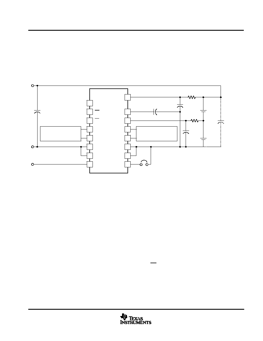
APPLICATION INFORMATION
Figure 1 shows a typical application for the UCC3911 Li-Ion and Li-Pol battery protector. All of the functions
required to protect two series cells from overvoltage and undervoltage conditions, as well as provide short circuit
protection for the complete battery pack, are included in a single chip. An internal state machine controls an
internal power FET which allows either bi-directional or uni-directional battery current. An optional time delay
capacitor can be included to slow the reaction time of the short circuit protection circuitry if desired.
While the device is capable of providing overload and over/undervoltage protection of both cells with virtually
no external parts, the demands of true short circuit protection require some passive external components.
UDG≠99173
1
3
2
4
5
7
6
8
16
14
15
13
12
10
11
9
NC
SUBS
SUBS
GND
LPWARN
GND
B2
CDLY
B1
SUBS
SUBS
B0
CE
B0
UCC3911
J1
ISOLATED COPPER PAD
FOR HEAT SINKING AT
HIGH LOAD CURRENTS
C2
0.22
µ
F
+
CELL 1
ENABLE (OPEN)
CDLY 330 pF
C1 10
µ
F
10 V
R1 220
+
CELL 2
C4
(OPTIONAL)
ISOLATED COPPER PAD
FOR HEAT SINKING AT
HIGH LOAD CURRENTS
C3 0.1
µ
F
25 V
R2 10 k
OV
UV
Figure 1. Application Circuit Including Components for Short-Circuit Protection
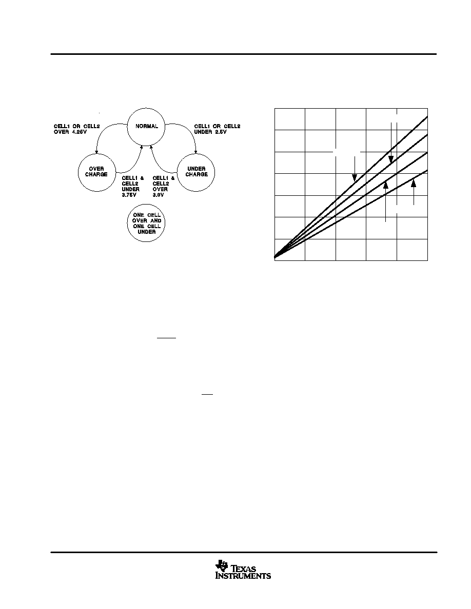
state machine operation
The internal state machine constantly monitors the two cells for both overvoltage and undervoltage conditions.
Figure 2 shows a state diagram which describes the operation of the protection circuitry for the UCC3911≠2
version. In the normal mode, both the external overvoltage and undervoltage status bits are held high and full
battery current is allowed through the internal power FET in either the charge or discharge direction.
If the voltage across one or both cells exceeds the overvoltage (V
OV
) threshold, the external overvoltage signal
goes low, and further charge current is not allowed. An internal feedback loop controls the power FET to allow
only discharge current, allowing for battery recovery. The state machine will not reenter normal mode until the
voltage across both cells decays to less than the overvoltage recovery (V
OVR
) threshold. This feature is
important to prevent circuit oscillation due to battery ESR when the circuitry transitions between states.
If the voltage across one or both battery cells falls below 3 V, the LPWARN signal goes high indicating a low
power condition. This signal can be used to signal the user that the battery pack is in need of charge.
If the voltage across one or both cells falls below 2.5 V, the UV signal goes low, and the feedback loop allows
only charge current. The LPWARN signal goes low and the UCC3911 enters sleep mode which consumes only
3
µ
A, limiting self discharge to a minimum. The circuit remains in this state until the voltage across both cells
exceeds 3 V. The battery pack can still be charged, unless the sum of the two cells voltages falls below 3.7 V,
which is the minimum guaranteed operating voltage for the device.

UCC3911-1, UCC3911-2
UCC3911-3, UCC3911-4
SLUS429B≠ FEBRUARY 2000 ≠ REVISED NOVEMBER 2002
8
www.ti.com
APPLICATION INFORMATION
If the battery cells become so poorly matched that the voltage across one cell exceeds 4.25 V and the voltage
across the other cell falls below 2.5 V, the power FET does not pass either charge or discharge current, and
both the OV and UV signals will be set low.
The normal high current path for battery current is through the B0 (10, 11) and GND (6, 7) pins of the UCC3911.
The GND pins are intended to be connected to system ground for either the charger or the load. The SUBS pins
(4, 5, 12, 13) are internally connected to the substrate of the UCC3911, which is internally referenced to B0 or
GND depending on the direction of pack current. If high battery currents are anticipated, the SUBS pins can be
thermally connected to a heat sink to control the device temperature. However, this heat sink must be electrically
isolated from all other device pins including ground. This is a critically important point, as heat sinking to the
system ground is not possible.
The CE pin is used to initialize the state of the battery pack during assembly. Holding this pin low forces the state
machine to hold the FET off. The last step in the assembly process would be to cut the trace between this pin
and B0 which allows the internal pull up to start the state machine. While CE is low, the device's current
consumption is approximately 4
µ
A. This is a useful feature for battery packs that may experience a long period
of storage while waiting to be sold.
The one cell over and one cell under state (see Figure 2) is entered whenever one cell is overcharged and the
other cell is simultaneously overdischarged. When in this state, the series FET switch is turned off inhibiting both
charging and discharging of the battery pack. If the battery pack ever gets into this condition, it should be
discarded.
short-circuit protection
The demands of true short-circuit protection require that careful attention be paid to the selection of a few
external components.
In the application circuit shown in Figure 1, C3 protects the battery pack output terminals from inductive kick
when the pack current is shut off due to an overcurrent or overvoltage/undervoltage condition. (It also increases
the ESD protection level.)
To prevent a momentary cell voltage drop, caused by large capacitive loads, from causing an erroneous
undervoltage shutdown, an RC filter is required in series with the two battery sense inputs, B1 and B2. The
resistors (R1 and R2) are sized to have a negligible impact on voltage sensing accuracy. The capacitors (C1
and C2) should be sized to provide a time constant longer than the overcurrent delay time. In the example of
Figure 1, they are sized for a nominal 2.2 ms time constant. They do not need to be low ESR style capacitors,
as they see no ripple current. A larger resistor value and smaller capacitor value can be used on the B1 input
due to the extremely low input current on this pin.
The overcurrent delay capacitor, CDLY, sets the time delay, after the overcurrent threshold is exceeded, before
turning off the UCC3911's internal FET. If no capacitor is used, the nominal delay is 100
µ
s. To charge large
capacitive loads without tripping the overcurrent circuit, a small capacitor (typically less than 1000 pF) is used
to extend the delay time. The approximate delay time is given below and shown graphically in Figure 3.
t
DLY
(
m
s)
+
25
)
(25
)
CDLY(pF) )
0.4
V
B2
(2)
UCC3911-1, UCC3911-2
UCC3911-3, UCC3911-4
SLUS429B≠ FEBRUARY 2000 ≠ REVISED NOVEMBER 2002
9
www.ti.com
APPLICATION INFORMATION
Figure 2
UCC3911≠2 STATE DIAGRAM
Figure 3
0
200
400
600
800
1000
500
0
1500
1000
2500
2000
3500
3000
VB2 = 7
VB2 = 8
VB2 = 5
VB2 = 6
Delay Capacitance (pF)
Delay T
ime (
µ
s)
NOMINAL OVERCURRENT DELAY TIME
vs
DELAY CAPACITANCE AND B2 VOLTAGE
The amount of time required will be a function of the load capacitance, battery voltage, and the total circuit
impedance, including the internal resistance of the cells, the UCC3911's on resistance, and the load capacitor
ESR. The required delay time can be calculated from:
t
+ *
R
C
ln I
R
V
In this equation, R is the total circuit resistance, C is the capacitor being charged, I is the overcurrent trip current
(5.25 A nominal), and V is the battery voltage. Using the minimum trip current of 3.5 A and the maximum battery
voltage of 8.4 V, the worst case maximum delay time required is defined as:
t
MAX
(
m
s)
+ *
R
C (
m
F)
ln
R
2.4
In the example of Figure 1, CDLY, C1 and C2 are sized to drive a 1500-
µ
F load capacitor.
If large capacitive loads (or other loads with surge currents above the overcurrent trip threshold) are not being
applied to the pack terminals, the overcurrent delay time can be short. In this case, it may be possible to eliminate
CDLY, as well as R2 and C2 altogether (replacing R2 with a short). In addition, the time constant of R1 and C1
can be made much shorter. R1 and C2 are still necessary, however, to assure proper operation under short
circuit conditions. It is important to maintain a minimum R1/C1 time constant of 100
µ
s. (For example, R1 and
C1 could be reduced to 100
and 1
µ
F.)
Capacitor C4 is recommended, in case the wires connecting to the top and bottom of the cell stack are more
than an inch long (not likely in a small battery pack). In this case, a 10-
µ
F, low ESR capacitor is recommended
to prevent excessive overshoot at turn-off due to wiring inductance.
(3)
(4)
PACKAGING INFORMATION
Orderable Device
Status
(1)
Package
Type
Package
Drawing
Pins Package
Qty
Eco Plan
(2)
Lead/Ball Finish
MSL Peak Temp
(3)
UCC3911DP-1
ACTIVE
SOIC
D
16
40
Green (RoHS &
no Sb/Br)
CU NIPDAU
Level-2-260C-1 YEAR
UCC3911DP-2
ACTIVE
SOIC
D
16
40
Green (RoHS &
no Sb/Br)
CU NIPDAU
Level-2-260C-1 YEAR
UCC3911DP-3
ACTIVE
SOIC
D
16
40
Green (RoHS &
no Sb/Br)
CU NIPDAU
Level-2-260C-1 YEAR
UCC3911DP-3G4
ACTIVE
SOIC
D
16
40
Green (RoHS &
no Sb/Br)
CU NIPDAU
Level-2-260C-1 YEAR
UCC3911DP-4
ACTIVE
SOIC
D
16
40
Green (RoHS &
no Sb/Br)
CU NIPDAU
Level-2-260C-1 YEAR
UCC3911DPTR-2G4
ACTIVE
SOIC
D
16
TBD
Call TI
Call TI
(1)
The marketing status values are defined as follows:
ACTIVE: Product device recommended for new designs.
LIFEBUY: TI has announced that the device will be discontinued, and a lifetime-buy period is in effect.
NRND: Not recommended for new designs. Device is in production to support existing customers, but TI does not recommend using this part in
a new design.
PREVIEW: Device has been announced but is not in production. Samples may or may not be available.
OBSOLETE: TI has discontinued the production of the device.
(2)
Eco
Plan
-
The
planned
eco-friendly
classification:
Pb-Free
(RoHS)
or
Green
(RoHS
&
no
Sb/Br)
-
please
check
http://www.ti.com/productcontent
for the latest availability information and additional product content details.
TBD: The Pb-Free/Green conversion plan has not been defined.
Pb-Free (RoHS): TI's terms "Lead-Free" or "Pb-Free" mean semiconductor products that are compatible with the current RoHS requirements
for all 6 substances, including the requirement that lead not exceed 0.1% by weight in homogeneous materials. Where designed to be soldered
at high temperatures, TI Pb-Free products are suitable for use in specified lead-free processes.
Green (RoHS & no Sb/Br): TI defines "Green" to mean Pb-Free (RoHS compatible), and free of Bromine (Br) and Antimony (Sb) based flame
retardants (Br or Sb do not exceed 0.1% by weight in homogeneous material)
(3)
MSL, Peak Temp. -- The Moisture Sensitivity Level rating according to the JEDEC industry standard classifications, and peak solder
temperature.
Important Information and Disclaimer:The information provided on this page represents TI's knowledge and belief as of the date that it is
provided. TI bases its knowledge and belief on information provided by third parties, and makes no representation or warranty as to the
accuracy of such information. Efforts are underway to better integrate information from third parties. TI has taken and continues to take
reasonable steps to provide representative and accurate information but may not have conducted destructive testing or chemical analysis on
incoming materials and chemicals. TI and TI suppliers consider certain information to be proprietary, and thus CAS numbers and other limited
information may not be available for release.
In no event shall TI's liability arising out of such information exceed the total purchase price of the TI part(s) at issue in this document sold by TI
to Customer on an annual basis.
PACKAGE OPTION ADDENDUM
www.ti.com
19-Oct-2005
Addendum-Page 1

IMPORTANT NOTICE
Texas Instruments Incorporated and its subsidiaries (TI) reserve the right to make corrections, modifications,
enhancements, improvements, and other changes to its products and services at any time and to discontinue
any product or service without notice. Customers should obtain the latest relevant information before placing
orders and should verify that such information is current and complete. All products are sold subject to TI's terms
and conditions of sale supplied at the time of order acknowledgment.
TI warrants performance of its hardware products to the specifications applicable at the time of sale in
accordance with TI's standard warranty. Testing and other quality control techniques are used to the extent TI
deems necessary to support this warranty. Except where mandated by government requirements, testing of all
parameters of each product is not necessarily performed.
TI assumes no liability for applications assistance or customer product design. Customers are responsible for
their products and applications using TI components. To minimize the risks associated with customer products
and applications, customers should provide adequate design and operating safeguards.
TI does not warrant or represent that any license, either express or implied, is granted under any TI patent right,
copyright, mask work right, or other TI intellectual property right relating to any combination, machine, or process
in which TI products or services are used. Information published by TI regarding third-party products or services
does not constitute a license from TI to use such products or services or a warranty or endorsement thereof.
Use of such information may require a license from a third party under the patents or other intellectual property
of the third party, or a license from TI under the patents or other intellectual property of TI.
Reproduction of information in TI data books or data sheets is permissible only if reproduction is without
alteration and is accompanied by all associated warranties, conditions, limitations, and notices. Reproduction
of this information with alteration is an unfair and deceptive business practice. TI is not responsible or liable for
such altered documentation.
Resale of TI products or services with statements different from or beyond the parameters stated by TI for that
product or service voids all express and any implied warranties for the associated TI product or service and
is an unfair and deceptive business practice. TI is not responsible or liable for any such statements.
Following are URLs where you can obtain information on other Texas Instruments products and application
solutions:
Products
Applications
Amplifiers
amplifier.ti.com
Audio
www.ti.com/audio
Data Converters
dataconverter.ti.com
Automotive
www.ti.com/automotive
DSP
dsp.ti.com
Broadband
www.ti.com/broadband
Interface
interface.ti.com
Digital Control
www.ti.com/digitalcontrol
Logic
logic.ti.com
Military
www.ti.com/military
Power Mgmt
power.ti.com
Optical Networking
www.ti.com/opticalnetwork
Microcontrollers
microcontroller.ti.com
Security
www.ti.com/security
Telephony
www.ti.com/telephony
Video & Imaging
www.ti.com/video
Wireless
www.ti.com/wireless
Mailing Address:
Texas Instruments
Post Office Box 655303 Dallas, Texas 75265
Copyright
2005, Texas Instruments Incorporated