
UCC2913
UCC3913
SLUS274A ≠ JANUARY 1999 ≠ REVISED APRIL 2003
NEGATIVE VOLTAGE HOT SWAP POWER MANAGER
1
www.ti.com
FEATURES
D
Precision Fault Threshold
D
Programmable Average Power Limiting
D
Programmable Linear Current Control
D
Programmable Overcurrent Limit
D
Programmable Fault Time
D
Fault Output Indicator
D
Shutdown Control
D
Undervoltage Lockout
D
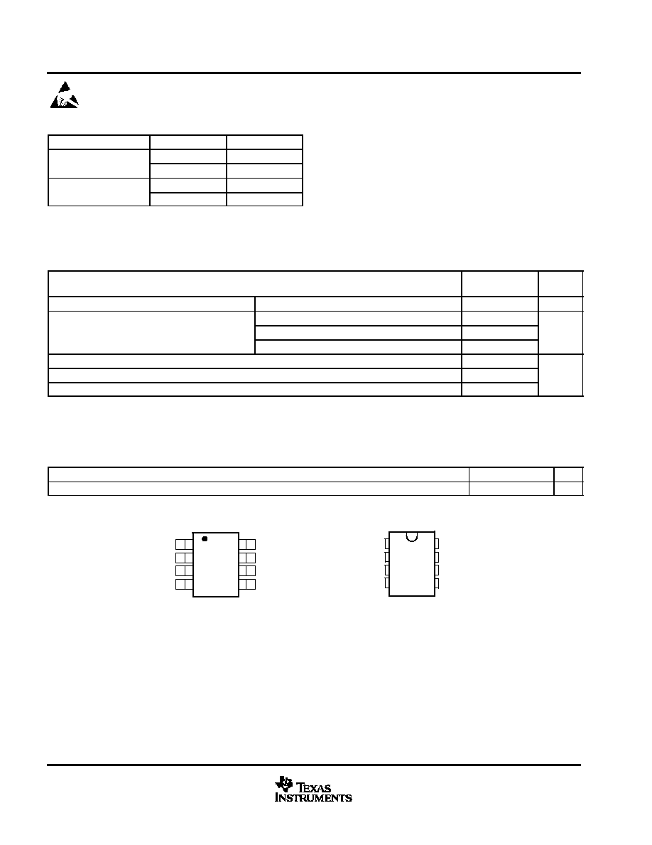
8-Pin SOIC
APPLICATIONS
D
≠48-V Distributed Power Systems
D
Central Office Switching
D
Wireless Base Stations
DESCRIPTION
The UCCx913 family of negative voltage circuit
breakers provides complete power management,
hot-swap, and fault handling capability. The
device is referenced to the negative input voltage
and is driven through an external resistor
connected to ground, which is essentially a
current drive as opposed to the traditional voltage
drive. The on-board 10-V shunt regulator protects
the device from excess voltage and serves as a
reference for programming the maximum
allowable output sourcing current during a fault. In
the event of a constant fault, the internal timer
limits the on-time from less than 0.1% to a
maximum of 3%. The duty cycle modulates
depending on the current into the PL pin, which is
a function of the voltage across the FET, and limits
average power dissipation in the FET. The fault
level is fixed at 50 mV across the current-sense
resistor to minimize total dropout. The fault current
level is set with an external current sense resistor.
The maximum allowable sourcing current is
programmed with a voltage divider from VDD to
generate a fixed voltage on the IMAX pin. The
current level, when the output appears as a
current source, is equal to V
IMAX
/R
SENSE
. If
desired, a controlled current startup can be
programmed with a capacitor on the IMAX pin.
When the output current is below the fault level,
the output device is switched on. When the output
current exceeds the fault level, but is less than the
maximum sourcing level programmed by the
IMAX pin, the output remains switched on, and the
fault timer starts charging CT. Once CT charges to
2.5 V, the output device is turned off and performs
a retry some time later. When the output current
reaches the maximum sourcing current level, the
output appears as a current source, limiting the
output current to the set value defined by IMAX.
Other features of the UCCx913 family include
undervoltage lockout, and 8-pin small outline
(SOIC) and dual-in-line (DIP) packages.
PRODUCTION DATA information is current as of publication date.
Products conform to specifications per the terms of Texas Instruments
standard warranty. Production processing does not necessarily include
testing of all parameters.
Copyright
1999 ≠ 2003, Texas Instruments Incorporated
1
8
7
6
5
≠VIN
3
UCC3913
2
4
Power
Limiting
Current
Control
Fault
Protection
and
Timer
DC/DC
Converter
or Load
RVDD
SIMPLIFIED APPLICATION DIAGRAM
RS
R1
R2
RPL
CT
CVDD
M1
UDG≠03059
UCC2913
UCC3913
SLUS274A ≠ JANUARY 1999 ≠ REVISED APRIL 2003
2
www.ti.com
These devices have limited built-in ESD protection. The leads should be shorted together or the device placed in conductive foam
during storage or handling to prevent electrostatic damage to the MOS gates.
ORDERING INFORMATION
TA
PACKAGE(1)
PART NUMBER
40
∞
C to 85
∞
C
PDIP (N)
UCC2913N
≠40
∞
C to 85
∞
C
SOIC (D)
UCC2913D
0
∞
C to 70
∞
C
PDIP (N)
UCC3913N
≠0
∞
C to 70
∞
C
SOIC (D)
UCC3913D
(1) The N and D packaged are also available taped and reeled.
Add an R suffix to the device type (i.e., UCC2913NR).
ABSOLUTE MAXIMUM RATINGS
over operating free-air temperature range unless otherwise noted(1)
UCC2923
UCC3913
UNIT
Input voltage
IMAX
limited to VDD
V
VDD
50
Input current
SHUTDOWN
10
mA
In ut current
PL
10
mA
Operating junction temperature range, TJ
≠55 to 150
Storage temperature, Tstg
≠65 to 150
∞
C
Lead temperature 1,6 mm (1/16 inch) from case for 10 seconds
300
C
(1) Stresses beyond those listed under "absolute maximum ratings" may cause permanent damage to the device. These are stress ratings only,
and functional operation of the device at these or any other conditions beyond those indicated under "recommended operating conditions" is
not implied. Exposure to absolute-maximum-rated conditions for extended periods may affect device reliability. All voltages are with respect to
VSS (the most negative voltage). All currents are positive into and negative out of the specified terminal.
RECOMMENDED OPERATING CONDITIONS
MIN
NOM
MAX
UNIT
Input current, IVDD
2
5
20
mA
1
2
3
4
8
7
6
5
SD/FLT
IMAX
VDD
CT
PL
OUT
SENSE
VSS
1
2
3
4
8
7
6
5
SD/FLT
IMAX
VDD
CT
PL
OUT
SENSE
VSS
N PACKAGE
(TOP VIEW)
D PACKAGE
(TOP VIEW)
UCC2913
UCC3913
SLUS274A ≠ JANUARY 1999 ≠ REVISED APRIL 2003
3
www.ti.com
ELECTRICAL CHARACTERISTICS
TA = ≠40
∞
C to 85
∞
C for UCC2913, TA = 0
∞
C to 70
∞
C for UCC3913, TJ = TA, IVDD = 2 mA, CT = 4.7 pF, TA = TJ (unless otherwise noted)
PARAMETER
TEST CONDITIONS
MIN
TYP
MAX
UNIT
INPUT SUPPLY
Minimum input current, VDD
1
2
mA
Regulator voltage
2 mA
ISOURCE
10 mA
8.5
9.5
10.5
V
Undervoltage lockout off-voltage
6
7
8
V
FAULT TIMING
Overcurrent threshold voltage
TJ = 25
∞
C
47.5
50.0
53.0
mV
Overcurrent threshold voltage
Over temperature
46.0
50.0
53.5
mV
Overcurrent input bias
50
500
nA
VCT = 1.0 V,
IPL = 0 A
≠22
≠36
≠50
µ
A
Timing capacitance charge current
Overload condition,
VSENSE ≠ VIMAX = 300 mV
≠0.7
≠1.2
≠1.7
mA
Timing capacitance discharge current
VCT = 1.0 V,
IPL = 0 A
0.6
1.0
1.5
µ
A
Timing capacitance fault threshold voltage
2.2
2.4
2.6
V
Timing capacitance reset threshold voltage
0.32
0.50
0.62
V
Output duty cycle
Fault condition,
IPL = 0 A
1.7%
2.7%
3.7%
OUTPUT
High le el o tp t oltage
IOUT = 0 A
8.5
10
High-level output voltage
IOUT = ≠1 A
6
8
Low level output voltage
IOUT = 0 A,
VSENSE ≠ VIMAX = 100mV
0.01
V
Low-level output voltage
IOUT = 2 A,
VSENSE ≠ VIMAX = 100mV
0.2
0.6
LINEAR AMPLIFIER
Sense control voltage
VIMAX = 100 mV
85
100
115
mV
Sense control voltage
VIMAX = 400 mV
370
400
430
mV
Input bias
50
500
nA
SHUTDOWN/FAULT
Shutdown threshold voltage
1.4
1.7
2.0
V
Input current
VSD/FLT = 5 V
15
25
45
µ
A
High-level output voltage
6.0
7.5
9.0
V
Low-level output voltage
0.01
V
Delay-to-output time
150
300
ns
POWER LIMITING
PL regulator voltage
IPL = 64
µ
A
4.35
4.85
5.35
V
Duty cycle control
IPL = 64
µ
A
0.6%
1.2%
1.7%
Duty cycle control
IPL = 1 mA
0.045%
0.1%
0.17%
OVERLOAD
Delay-to-output time
300
500
ns
Output sink current
VSENSE ≠ VIMAX = 300mV
40
100
mA
Overload threshold voltage
Relataive to IIMAX
140
200
260
mV
UCC2913
UCC3913
SLUS274A ≠ JANUARY 1999 ≠ REVISED APRIL 2003
4
www.ti.com
TERMINAL FUNCTIONS
TERMINAL
I/O
DESCRIPTION
NAME
NO.
I/O
DESCRIPTION
CT
4
I
A capacitor is connected to this pin in order to set the maximum fault time.
IMAX
2
I
This pin programs the maximum allowable sourcing current.
OUT
7
O
Output drive to the MOSFET pass element.
PL
8
I
This feature ensures that the average MOSFET power dissipation is controlled.
SENSE
6
I
Input voltage from the current sense resistor.
SD/FLT
1
O
This pin provides fault output indication and shutdown control.
VDD
3
O
Current driven with a resistor to a voltage at least 10V more positive than VSS.
VSS
5
O
Ground reference for the device and the most negative voltage available.
DETAILED PIN DESCRIPTIONS
CT
A capacitor connected to this pin allows setting of the maximum fault time. The maximum fault time must be
more than the time to charge external load capacitance. The maximum fault time is defined as:
t
FAULT
+
2
C
T
I
CH
where
I
CH
+
36
m
A
)
I
PL
and I
PL
is the current into the power limit pin. Once the fault time is reached the output shuts down for a time
given by:
t
SD
+
2
10
6
C
T
IMAX
This pin programs the maximum allowable sourcing current. Since V
DD
is a regulated voltage, a voltage divider
can be derived from V
DD
to generate the program level for the IMAX pin. The current level at which the output
appears as a current source is equal to the voltage on the IMAX pin over the current sense resistor. If desired,
a controlled current startup can be programmed with a capacitor on the IMAX pin, and a programmed start delay
can be achieved by driving the shutdown with an open collector/drain device into an R-C network.
PL
This pin's feature ensures that the average MOSFET power dissipation is controlled. A resistor is connected
from this pin to the drain of the N-channel MOSFET pass element. When the voltage across the N-channel
MOSFET exceeds 5 V, current flows into the PL pin which adds to the fault timer charge current, reducing the
duty cycle from the 3% level. When I
PL
is much greater 36
µ
A, then the average MOSFET power dissipation
is given by:
P
FET(avg)
+
IMAX
1
10
*
6
R
PL
SENSE
Input voltage from the current sense resistor. When there is greater than 50 mV across this pin with respect to
VSS, a fault is sensed, and C
T
starts to charge.
(1)
(2)
(3)
(4)
UCC2913
UCC3913
SLUS274A ≠ JANUARY 1999 ≠ REVISED APRIL 2003
5
www.ti.com
DETAILED PIN DESCRIPTIONS (continued)
SD/FLT
This pin provides fault output indication and shutdown control. Interface into and out of this pin is usually
performed through level shift transistors. When 20
µ
A is sourced into this pin, shutdown drives high causing the
output to disable the N-channel MOSFET pass device. When opened, and under a non-fault condition, the
SD/FLT pin pulls to a low state. When a fault is detected by the fault timer, or undervoltage lockout, this pin drives
to a high state, indicating the output MOSFET is off.
VDD
Current driven with a resistor to a voltage at least 10-V more positive than VSS. Typically a resistor is connected
to ground. The 10-V shunt regulator clamps VDD at 10 V above the VSS pin, and is also used as an output
reference to program the maximum allowable sourcing current.
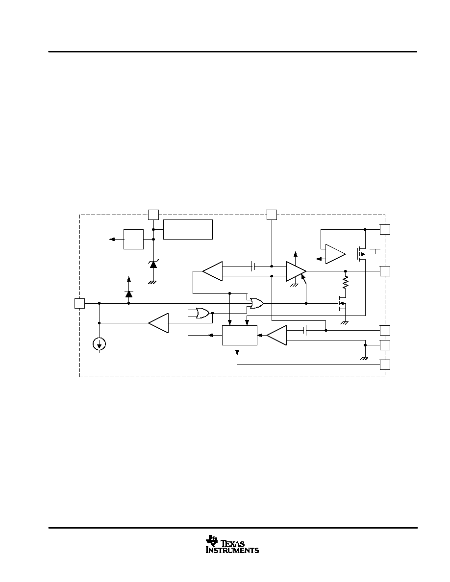
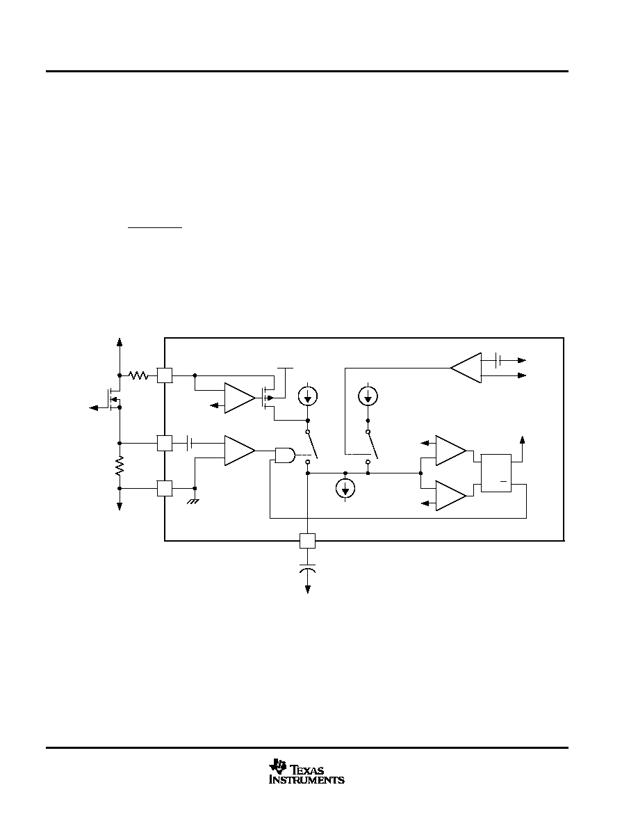
BLOCK DIAGRAM
1
2
LINEAR
CURRENT
AMPLIFIER
PL
7
OUT
+
≠
+
≠
IMAX
+
8
+
≠
6
SENSE
5
VSS
4
CT
ON≠TIME
CONTROL
3
VDD
UVLO
5.0V
REF
LOGIC
SUPPLY
+
1= UNDERVOLTAGE
+
≠
SOURCE
ONLY
SD/FLT
VDD
0.2 V
OVERCURRENT
COMPARATOR
DISABLE
5.0 V
OVERLOAD COMPARATOR
50 mV
UDG≠99001
50
VDD
VDD
20
µ
A
9.5-V SHUNT
REGULATOR
UCC2913
UCC3913
SLUS274A ≠ JANUARY 1999 ≠ REVISED APRIL 2003
6
www.ti.com
APPLICATION INFORMATION
Typical Fault Mode
Figure 1 shows the detailed circuitry for the fault timing function of the UCCx913. This initial discussion of the
typical fault mode ignores the overload comparator, and current source I3. Once the voltage across the current
sense resistor, R
S
, exceeds 50 mV, a fault has occurred. This causes the timing capacitor to charge with a
combination of 36
µ
A plus the current from the power limiting amplifier. The PL amplifier is designed to source
current into the CT pin only and to begin sourcing current once the voltage across the output FET exceeds 5 V.
The current I
PL
is related to the voltage across the FET with the following expression:
I
PL
+
V
FET
*
5 V
R
PL
where V
FET
is the voltage across the N-channel MOSFET pass device.
(How this feature limits average power dissipation in the pass device is described in further detail in the following
sections). Note that under a condition where the output current is more than the fault level, but less than the
maximum level, V
OUT
V
SS
(input voltage), I
PL
= 0, the C
T
charging current is 36
µ
A.
UDG≠99004
8
5
6
4
OVERCURRENT
COMPARATOR
PL
+
≠
SENSE
VSS
VSS
INPUT VOLTAGE
OUTPUT
LOAD
I1
+
≠
+
S
Q
Q
R
H=CLOSE
I2
I3
1mA
+
≠
+
SENSE
IMAX
+
≠
+
≠
H=CLOSE
0.5 V
2.5 V
CT
VSS
TO OUTPUT
DRIVE
H=OFF
OVERLOAD COMPARATOR
CT
FAULT TIMING CIRCUITRY
0.2 V
50 mV
VDD
RPL
RS
5.0 V
1
µ
A
36
µ
A
Figure 1. Fault Timing Circuitry Including Power Limit and Overload Comparator
(5)
UCC2913
UCC3913
SLUS274A ≠ JANUARY 1999 ≠ REVISED APRIL 2003
7
www.ti.com
APPLICATION INFORMATION
During a fault, C
T
charges at a rate determined by the internal charging current and the external timing capacitor.
Once C
T
charges to 2.5 V, the fault comparator switches and sets the fault latch. Setting of the fault latch causes
both the output to switch off and the charging switch to open. C
T
must now discharge with the 1-
µ
A current
source, I2, until 0.5 V is reached. Once the voltage at CT reaches 0.5 V, the fault latch resets, which re-enables
the output and allows the fault circuitry to regain control of the charging switch. If a fault is still present, the fault
comparator closes the charging switch causing the cycle to begin. Under a constant fault, the duty cycle is given
by:
Duty Cycle
+
1
m
A
I
PL
)
36
m
A
Average power dissipation in the pass element is given by:
P
FET(avg)
+
V
FET
IMAX
1
m
A
I
PL
)
36
m
A
Where VFET >> 5 V I
PL
can be approximated as :
I
PL
^
V
FET
R
PL
and where I
PL
>> 36
µ
A, the duty cycle can be approximated as :
Duty Cycle
+
1
m
A
R
PL
V
FET
Therefore, the maximum average power dissipation in the MOSFET can be approximated by:
P
FET(avg)
+
V
FET
IMAX
1
m
A
R
PL
V
FET
+
IMAX
1
m
A
R
PL
Notice that in the approximation, V
FET
cancels. therefore, average power dissipation is limited in the N-channel
MOSFET pass element.
Overload Comparator
The linear amplifier in the UCCx913 ensures that the output N-channel MOSFET does not pass more than I
MAX
(which is V
IMAX
/R
S
). In the event the output current exceeds the programmed IMAX by 0.2 V/R
S (
which can only
occur if the output MOSFET is not responding to a command from the device) the CT pin begins charging with
I3, 1 mA, and continue to charge to approximately 8 V. This allows a constant fault to show up on the SD/FLT
pin, and also since the voltage on CT charges past 2.5 V only in an overload fault mode, it can be used for
detection of output FET failure or to build in redundancy in the system.
(6)
(7)
(8)
(9)
(10)
UCC2913
UCC3913
SLUS274A ≠ JANUARY 1999 ≠ REVISED APRIL 2003
8
www.ti.com
APPLICATION INFORMATION
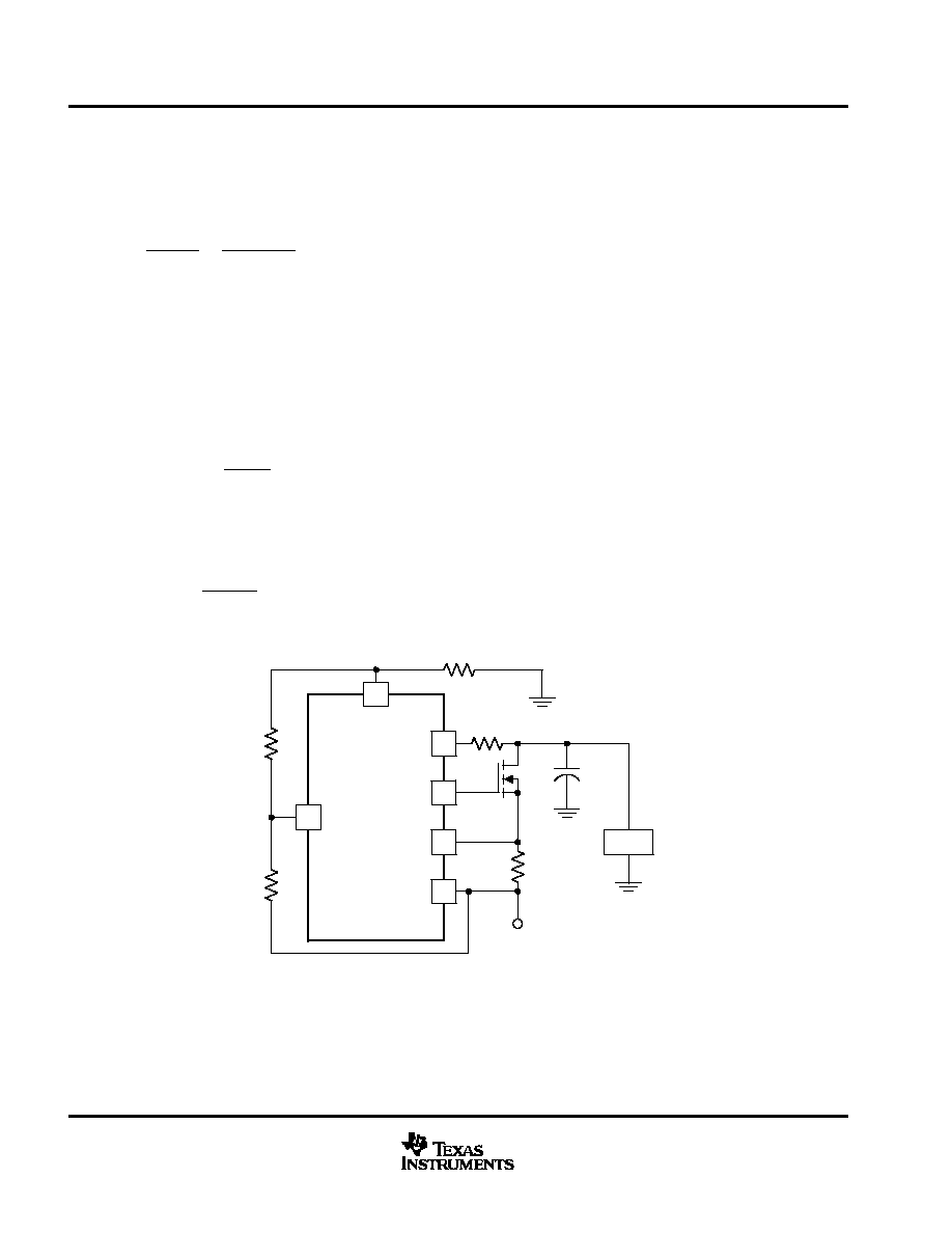
Determining External Component Values (See FIgure 2)
To set R
VDD
the following must be achieved:
V
IN(min)
R
VDD
u
10 V
(R1
)
R2)
)
2 mA
In order to estimate the minimum timing capacitor, C
T
, several things must be taken into account. For example,
given the schematic below as a possible (and at this point, a standard) application, certain external component
values must be known in order to estimate C
T(min)
.
Then use the given the values of C
OUT
, Load, R
SENSE
, VSS, and the resistors determining the voltage on the
IMAX pin, to calculate the approximate startup time of the node V
OUT
. This startup time must be faster than the
time it takes for CT to charge to 2.5 V (relative to VSS), and is the basis for estimating the minimum value of
CT. In order to determine the value of the sense resistor, R
SENSE
, assuming the user has determined the fault
current, R
SENSE
can be calculated by:
R
SENSE
+
50 mV
I
FAULT
Next, calculate the variable I
MAX
. I
MAX
is the maximum current that the device allows through the transistor, M1,
and during startup with an output capacitor the power MOSFET, M1, can be modeled as a constant current
source of value I
MAX
where:
I
MAX
+
V
IMAX
R
SENSE
where V
IMAX
= voltage on IMAX pin.
UDG≠03045
RVDD
COUT
Note: LOAD = ILOAD For Current Source Load
LOAD = ROUT For Resistive Load
RPL
RSENSE
2
8
7
6
5
PL
OUT
SENSE
VSS
IMAX
UCC3913
3
VDD
VSS
LOAD
R1
R2
M1
VOUT
Figure 2. External Component Connections
(11)
(12)
(13)
UCC2913
UCC3913
SLUS274A ≠ JANUARY 1999 ≠ REVISED APRIL 2003
9
www.ti.com
APPLICATION INFORMATION
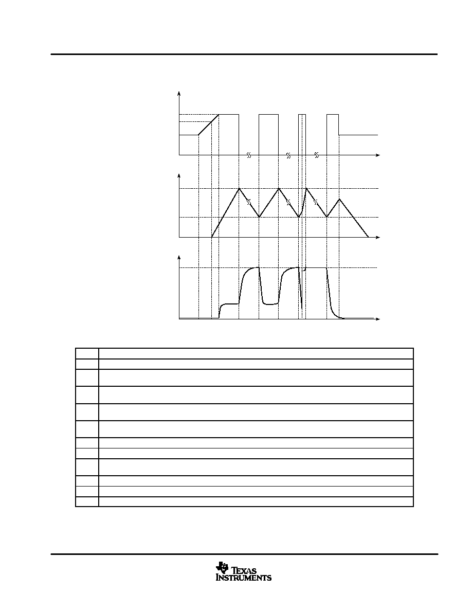
TIMING DIAGRAM
I
OUT
I
MAX
I
FAULT
Io(nom)
0A
V
CT
2.5V
0.5V
0V
0V
V
OUT
VSS
t
0
t
1
t
2
t
3
t
4
t
5
t
6
t
7
t
8
t
9
t
10
t
t
t
Output
Current
C
T
Voltage
(w/respect to VSS)
Output
Voltage
(w/respect to GND)
TIME
DESCRIPTION
TIME
DESCRIPTION
t0
Safe condition. Output current is nominal, output voltage is at the negative rail, VSS.
t1
Fault control reached. Output current reaches the programmed fault value. CT begins to charge at approximately
36-
µ
A.
t2
Maximum current reached. Output current reaches the programmed maximum level and becomes a constant current
with value IMAX.
t3
Fault occurs. CT has charged to 2.5V. Fault output goes high. The FET turns off allowing no output current to flow.
VOUT floats up to ground.
t4
Retry. CT has discharged to 0.5 V, but fault current is still exceeded, CT begins charging again, FET is on, VOUT pulled
down to VSS.
t5
t5 = t3. Illustrates 3% duty cycle.
t6
t6 = t4
t7
Output short circuit. If VOUT is short circuited to ground, CT charges at a higher rate depending upon the values for
VSS and RPL.
t8
Fault occurs. Output is still short circuited, but the occurrence of a fault turns the FET off so no current is conducted.
t9
t9 = t4. Output short circuit released, still in fault mode.
t10
t10 = t0. Fault released. Safe condition. Return to normal operaton of the circuit breaker.

UCC2913
UCC3913
SLUS274A ≠ JANUARY 1999 ≠ REVISED APRIL 2003
10
www.ti.com
APPLICATION INFORMATION
UDG≠99002
VDD
RVDD
50
1
2
LINEAR
CURRENT
AMPLIFIER
PL
7
OUT
+
≠
+
≠
IMAX
+
8
+
≠
6
SENSE
5
VSS
4
CT
ON≠TIME
CONTROL
3
VDD
UVLO
5.0 V
REF
LOGIC
SUPPLY
+
+
≠
SOURCE
ONLY
SD/FLT
R2
VSS
R1
OUTPUT
VSS
FAULT=
50 mV
DISABLE
9.5 SHUNT
REGULATOR
1 = UNDERVOLTAGE
VDD
RT
RS
CT
VDD
CSS
CVDD
20
µ
A
Figure 3. Typical Application Diagram
To calculate the startup time using the current source load.
t
START
+
C
OUT
|VSS|
I
MAX
*
I
LOAD
To calculate the startup time using the resistive load.
t
START
+
C
OUT
R
OUT
ln
I
MAX
R
OUT
I
MAX
R
OUT
*
|VSS|
(14)
(15)
UCC2913
UCC3913
SLUS274A ≠ JANUARY 1999 ≠ REVISED APRIL 2003
11
www.ti.com
APPLICATION INFORMATION
Once t
START
is calculated, the power limit feature of the UCCx913 must be addressed and component values
derived. Assuming the designer chooses to limit the maximum allowable average power that is associated with
the circuit breaker, the power limiting resistor, R
PL
, can be easily determined by the following:
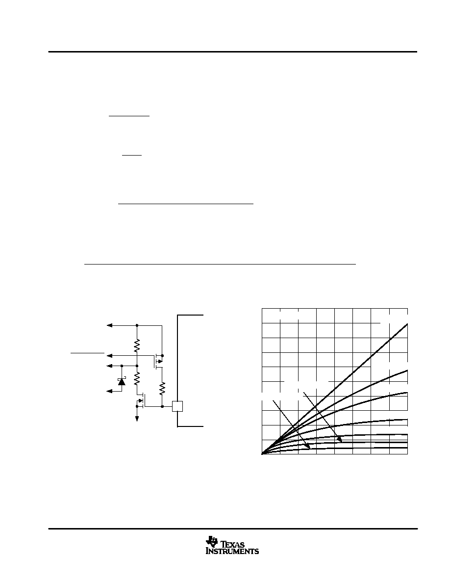
R
PL
+
P
FET(avg)
1
m
A
I
MAX
where a minimum R
PL
exists defined by
R
PL(min)
+
|VSS|
10mA
Finally, after computing the aforementioned variables, the minimum timing capacitor can be derived for a current
source load with the following equation.
C
T(min)
+
t
START
98
m
A
R
PL
)
|VSS|
*
10 V
4 V
R
PL
The minimum timing capacitor can be derived for a resistive load with the following equation.
C
T(min)
+
t
START
49
m
A
R
PL
)
|VSS|
*
5 V
*
I
MAX
R
OUT
)
R
OUT
C
OUT
|VSS|
2 V
R
PL
Figure 4. Possible Level Shift Circuitry Interface
UDG≠99003
SHUTDOWN
SD/FLT
7
R4
R3
VSS
LEVEL SHIFT
LOCAL VDD
LOCAL GND
FAULT OUT
UCC2913
UCC3913
0
2.5
0
75
5.0
10.0
7.5
12.5
17.5
15.0
20.0
25.0
22.5
25
50
100
175
125
150
200
Figure 5
IMAX = 4 A
RPL =
VFET ≠ MOSFET Voltage≠ V
P
AV
G
≠
A
verage Power Dissipation
≠
W
AVERAGE POWER DISSIPATION
vs
MOSFET VOLTAGE
RPL = 10 M
RPL = 5 M
RPL = 2 M
RPL = 1 M
RPL = 500 k
RPL = 200 k
(16)
(17)
(18)
(19)

UCC2913
UCC3913
SLUS274A ≠ JANUARY 1999 ≠ REVISED APRIL 2003
12
www.ti.com
SAFETY RECOMMENDATION
Although the UCC3913 is designed to provide system protection for all fault conditions, all integrated circuits
can ultimately fail short. For this reason, if the UCC3913 is intended for use in safety critical applications where
UL or some other safety rating is required, a redundant safety device such as a fuse should be placed in series
with the device. The UCC3913 will prevent the fuse from blowing for virtually all fault conditions, increasing
system reliability and reducing maintenance cost, in addition to providing the hot swap benefits of the device.
PACKAGING INFORMATION
Orderable Device
Status
(1)
Package
Type
Package
Drawing
Pins Package
Qty
Eco Plan
(2)
Lead/Ball Finish
MSL Peak Temp
(3)
UCC2913D
ACTIVE
SOIC
D
8
75
None
CU NIPDAU
Level-1-220C-UNLIM
UCC2913DTR
ACTIVE
SOIC
D
8
2500
None
CU NIPDAU
Level-1-220C-UNLIM
UCC2913DTRG4
PREVIEW
SOIC
D
8
2500 Green (RoHS &
no Sb/Br)
CU NIPDAU
Level-2-260C-1 YEAR
UCC2913J
OBSOLETE
CDIP
JG
8
None
Call TI
Call TI
UCC2913N
ACTIVE
PDIP
P
8
50
Pb-Free
(RoHS)
CU NIPDAU
Level-NC-NC-NC
UCC3913D
ACTIVE
SOIC
D
8
75
None
CU NIPDAU
Level-1-220C-UNLIM
UCC3913DTR
ACTIVE
SOIC
D
8
2500
None
CU NIPDAU
Level-1-220C-UNLIM
UCC3913N
ACTIVE
PDIP
P
8
50
Pb-Free
(RoHS)
CU NIPDAU
Level-NC-NC-NC
(1)
The marketing status values are defined as follows:
ACTIVE: Product device recommended for new designs.
LIFEBUY: TI has announced that the device will be discontinued, and a lifetime-buy period is in effect.
NRND: Not recommended for new designs. Device is in production to support existing customers, but TI does not recommend using this part in
a new design.
PREVIEW: Device has been announced but is not in production. Samples may or may not be available.
OBSOLETE: TI has discontinued the production of the device.
(2)
Eco Plan - May not be currently available - please check
http://www.ti.com/productcontent
for the latest availability information and additional
product content details.
None: Not yet available Lead (Pb-Free).
Pb-Free (RoHS): TI's terms "Lead-Free" or "Pb-Free" mean semiconductor products that are compatible with the current RoHS requirements
for all 6 substances, including the requirement that lead not exceed 0.1% by weight in homogeneous materials. Where designed to be soldered
at high temperatures, TI Pb-Free products are suitable for use in specified lead-free processes.
Green (RoHS & no Sb/Br): TI defines "Green" to mean "Pb-Free" and in addition, uses package materials that do not contain halogens,
including bromine (Br) or antimony (Sb) above 0.1% of total product weight.
(3)
MSL, Peak Temp. -- The Moisture Sensitivity Level rating according to the JEDECindustry standard classifications, and peak solder
temperature.
Important Information and Disclaimer:The information provided on this page represents TI's knowledge and belief as of the date that it is
provided. TI bases its knowledge and belief on information provided by third parties, and makes no representation or warranty as to the
accuracy of such information. Efforts are underway to better integrate information from third parties. TI has taken and continues to take
reasonable steps to provide representative and accurate information but may not have conducted destructive testing or chemical analysis on
incoming materials and chemicals. TI and TI suppliers consider certain information to be proprietary, and thus CAS numbers and other limited
information may not be available for release.
In no event shall TI's liability arising out of such information exceed the total purchase price of the TI part(s) at issue in this document sold by TI
to Customer on an annual basis.
PACKAGE OPTION ADDENDUM
www.ti.com
4-Mar-2005
Addendum-Page 1

MECHANICAL DATA
MCER001A ≠ JANUARY 1995 ≠ REVISED JANUARY 1997
POST OFFICE BOX 655303
∑
DALLAS, TEXAS 75265
JG (R-GDIP-T8)
CERAMIC DUAL-IN-LINE
0.310 (7,87)
0.290 (7,37)
0.014 (0,36)
0.008 (0,20)
Seating Plane
4040107/C 08/96
5
4
0.065 (1,65)
0.045 (1,14)
8
1
0.020 (0,51) MIN
0.400 (10,16)
0.355 (9,00)
0.015 (0,38)
0.023 (0,58)
0.063 (1,60)
0.015 (0,38)
0.200 (5,08) MAX
0.130 (3,30) MIN
0.245 (6,22)
0.280 (7,11)
0.100 (2,54)
0
∞
≠15
∞
NOTES: A. All linear dimensions are in inches (millimeters).
B. This drawing is subject to change without notice.
C. This package can be hermetically sealed with a ceramic lid using glass frit.
D. Index point is provided on cap for terminal identification.
E. Falls within MIL STD 1835 GDIP1-T8

MECHANICAL DATA
MPDI001A ≠ JANUARY 1995 ≠ REVISED JUNE 1999
POST OFFICE BOX 655303
∑
DALLAS, TEXAS 75265
P (R-PDIP-T8)
PLASTIC DUAL-IN-LINE
8
4
0.015 (0,38)
Gage Plane
0.325 (8,26)
0.300 (7,62)
0.010 (0,25) NOM
MAX
0.430 (10,92)
4040082/D 05/98
0.200 (5,08) MAX
0.125 (3,18) MIN
5
0.355 (9,02)
0.020 (0,51) MIN
0.070 (1,78) MAX
0.240 (6,10)
0.260 (6,60)
0.400 (10,60)
1
0.015 (0,38)
0.021 (0,53)
Seating Plane
M
0.010 (0,25)
0.100 (2,54)
NOTES: A. All linear dimensions are in inches (millimeters).
B. This drawing is subject to change without notice.
C. Falls within JEDEC MS-001
For the latest package information, go to http://www.ti.com/sc/docs/package/pkg_info.htm

IMPORTANT NOTICE
Texas Instruments Incorporated and its subsidiaries (TI) reserve the right to make corrections, modifications,
enhancements, improvements, and other changes to its products and services at any time and to discontinue
any product or service without notice. Customers should obtain the latest relevant information before placing
orders and should verify that such information is current and complete. All products are sold subject to TI's terms
and conditions of sale supplied at the time of order acknowledgment.
TI warrants performance of its hardware products to the specifications applicable at the time of sale in
accordance with TI's standard warranty. Testing and other quality control techniques are used to the extent TI
deems necessary to support this warranty. Except where mandated by government requirements, testing of all
parameters of each product is not necessarily performed.
TI assumes no liability for applications assistance or customer product design. Customers are responsible for
their products and applications using TI components. To minimize the risks associated with customer products
and applications, customers should provide adequate design and operating safeguards.
TI does not warrant or represent that any license, either express or implied, is granted under any TI patent right,
copyright, mask work right, or other TI intellectual property right relating to any combination, machine, or process
in which TI products or services are used. Information published by TI regarding third-party products or services
does not constitute a license from TI to use such products or services or a warranty or endorsement thereof.
Use of such information may require a license from a third party under the patents or other intellectual property
of the third party, or a license from TI under the patents or other intellectual property of TI.
Reproduction of information in TI data books or data sheets is permissible only if reproduction is without
alteration and is accompanied by all associated warranties, conditions, limitations, and notices. Reproduction
of this information with alteration is an unfair and deceptive business practice. TI is not responsible or liable for
such altered documentation.
Resale of TI products or services with statements different from or beyond the parameters stated by TI for that
product or service voids all express and any implied warranties for the associated TI product or service and
is an unfair and deceptive business practice. TI is not responsible or liable for any such statements.
Following are URLs where you can obtain information on other Texas Instruments products and application
solutions:
Products
Applications
Amplifiers
amplifier.ti.com
Audio
www.ti.com/audio
Data Converters
dataconverter.ti.com
Automotive
www.ti.com/automotive
DSP
dsp.ti.com
Broadband
www.ti.com/broadband
Interface
interface.ti.com
Digital Control
www.ti.com/digitalcontrol
Logic
logic.ti.com
Military
www.ti.com/military
Power Mgmt
power.ti.com
Optical Networking
www.ti.com/opticalnetwork
Microcontrollers
microcontroller.ti.com
Security
www.ti.com/security
Telephony
www.ti.com/telephony
Video & Imaging
www.ti.com/video
Wireless
www.ti.com/wireless
Mailing Address:
Texas Instruments
Post Office Box 655303 Dallas, Texas 75265
Copyright
2005, Texas Instruments Incorporated