 | –≠–ª–µ–∫—Ç—Ä–æ–Ω–Ω—ã–π –∫–æ–º–ø–æ–Ω–µ–Ω—Ç: UCC3917 | –°–∫–∞—á–∞—Ç—å:  PDF PDF  ZIP ZIP |
UCC1917
UCC2917
UCC3917
SLUS203A - AUGUST 1999
FEATURES
∑ Manages Hot Swap of 15V and
Above
∑ Precision Fault Threshold
∑ Programmable Average Power
Limiting
∑ Programmable Linear Current
Control
∑ Programmable Overcurrent Limit
∑ Programmable Fault Time
∑ Internal Charge Pump to Control
External NMOS Device
∑ Fault Output and Catastrophic
Fault Indication
∑ Fault Mode Programmable to
Latch or Retry
∑ Shutdown Control
∑ Undervoltage Lockout
Positive Floating Hot Swap Power Manager
12
11
8
7
6
5
10
4
2
3
1
13
16
9
15
14
5V
VOUT
V
DD
VDD
VOUT
DISABLE
OUTPUT
LOW
ON-TIME
DELAY
V
DD
40
µA
VOUT
UVLO
>10V=ENABLE
< 6V=DISABLE
5V
REFERENCE
LOGIC
SUPPLY
SHTDWN
FLTOUT
C1P
C1N
C2P
C2N
VSS
VREF/CATFLT
MAXI
CT
VOUT
SENSE
OUTPUT
PLIM
LATCH
VDD
+
200mV
OVER
CURRENT
COMPARATOR
40
µA
+
50mV
4V
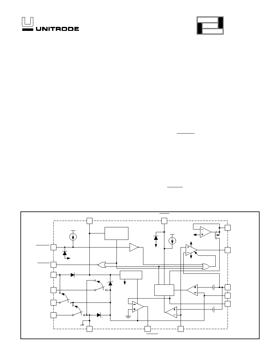
BLOCK DIAGRAM
UDG-99055
DESCRIPTION
The UCC3917 family of positive floating hot swap managers provides complete
power management, hot swap, and fault handling capability. The voltage limita-
tion of the application is only restricted by the external component voltage limi-
tations. The IC provides its own supply voltage via a charge pump off of VOUT.
The onboard 10V shunt regulator protects the IC from excess voltage. The IC
also has catastrophic fault indication to alert the user that the ability to shut off
the output NMOS has been bypassed. All control and housekeeping functions
are integrated and externally programmable. These include the fault current
level, maximum output sourcing current, maximum fault time, soft start time,
and average NMOS power limiting.
The fault level across the current sense amplifier is fixed at 50mV to minimize
total drop out. Once 50mV is exceeded across the current sense resistor, the
fault timer will start. The maximum allowable sourcing current is programmed
with a voltage divider from the VREF/CATFLT pin to generate a fixed voltage
on the MAXI pin. The current level at which the output appears as a current
source is equal to V
MAXI
divided by the current sense resistor. If desired, a con-
trolled current startup can be programmed with a capacitor on MAXI.
When the output current is below the fault level, the output device is switched
on with full gate drive. When the output current exceeds the fault level, but is
less than maximum allowable sourcing level programmed by MAXI, the output
remains switched on, and the fault timer starts charging CT. Once CT charges
to 2.5V, the output device is turned off and attempts either a retry sometime
later or waits for the state on the LATCH pin to change if in latch mode. When
the output current reaches the maximum sourcing current level, the output de-
vice appears as a current source.
application
INFO
available
2
UCC1917
UCC2917
UCC3917
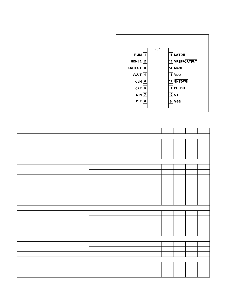
CONNECTION DIAGRAM
ELECTRICAL CHARACTERISTICS:
Unless otherwise specified, T
A
= 0∞C to 70∞C for the UCC3917, ≠40∞C to 85∞ for the
UCC2917 and ≠55∞C to 125∞C for the UCC1917, C
T
= 4.7nF. T
A
= T
J
. All voltages are with respect to VOUT. Current is positive
into and negative out of the specified terminal.
PARAMETER
TEST CONDITIONS
MIN
TYP
MAX
UNITS
VDD Section
I
DD
From VOUT (Note 1)
3.0
5
11
mA
UVLO Turn On Threshold
7.9
8.8
9.7
V
UVLO Off Voltage
5.5
6.5
7.5
V
VSS Regulator Voltage
≠6
≠5
≠4
V
Fault Timing Section
Overcurrent Threshold
T
A
= 25∞C
47.5
50
53
mV
Over Operating Temperature
46
50
54
mV
Overcurrent Input Bias
50
500
nA
CT Charge Current
V
CT
= 1V
≠78
≠50
≠28
µA
CT Catastrophic Fault Threshold
3.4
4.5
V
CT Fault Threshold
2.25
2.5
2.75
V
CT Reset Threshold
0.32
0.5
0.62
V
Output Duty Cycle
Fault Condition
1.7
2.7
3.7
%
Output Section
Output High Voltage
I
OUT
= 0
6
8
10
V
I
OUT
= ≠500
µA
5
7
9
V
Output Low Voltage
I
OUT
= 0
0
0.05
V
I
OUT
= 500
µA
0.1
0.5
V
I
OUT
= 1mA
0.5
0.9
V
Linear Current Section
Sense Control Votlage
MAXI = 100mV
85
100
115
mV
MAXI = 400mV
370
400
430
mV
Input Bias
MAXI = 200mV
50
500
nA
SHUTDOWN Section
Shutdown Threshold
2.0
2.4
2.8
V
Input Current
SHTDWN = 0V
24
40
60
µA
Shutdown Delay
100
500
ns
DIL-16, SOIC-16 (Top View)
J or N Package, D Package
IDD . . . . . . . . . . . . . . . . . . . . . . . . . . . . . . . . . . . . . . . . . . 20mA
SHTDWN Current . . . . . . . . . . . . . . . . . . . . . . . . . . . . . ≠500
µA
LATCH Current . . . . . . . . . . . . . . . . . . . . . . . . . . . . . . . ≠500
µA
VREF Current . . . . . . . . . . . . . . . . . . . . . . . . . . . . . . . . ≠500
µA
PLIM Current . . . . . . . . . . . . . . . . . . . . . . . . . . . . . . . . . . 10mA
MAXI Input Voltage . . . . . . . . . . . . . . . . . . . . . . . . . VDD + 0.3V
Storage Temperature . . . . . . . . . . . . . . . . . . . ≠65∞C to +150∞C
Junction Temperature . . . . . . . . . . . . . . . . . . . ≠55∞C to +150∞C
Lead Temperature (Soldering, 10 sec.) . . . . . . . . . . . . . +300∞C
Currents are positive into, negative out of the specified
terminal. Consult Packaging Section of Databook for thermal
limitations and considerations of package.
ABSOLUTE MAXIMUM RATINGS
3
UCC1917
UCC2917
UCC3917
ELECTRICAL CHARACTERISTICS:
Unless otherwise specified, T
A
= 0∞C to 70∞C for the UCC3917, ≠40∞C to 85∞ for
the UCC2917 and ≠55∞C to 125∞C for the UCC1917, C
T
= 4.7nF. T
A
= T
J
. All voltages are with respect to VOUT. Current is
positive into and negative out of the specified terminal.
PARAMETER
TEST CONDITIONS
MIN
TYP
MAX
UNITS
LATCH Section
Latch Threshold
1.7
2
2.3
V
Input Current
LATCH = 0V
24
40
60
µA
Fault Out Section
Fault Output High
6
8
10
V
Fault Output Low
0.01
0.05
V
Power Limiting Section
V
SENSE
Regulator Voltage
I
PLIMIT
= 64
µA
4.5
5
5.5
V
Duty Cycle Control
I
PLIMIT
= 64
µA
0.6
1.2
1.7
%
I
PLIMIT
= 1mA
0.045
0.1
0.2
%
VREF/CATFLT Section
V
REF
Regulator Voltage
4.5
5
5.5
V
Fault Output Low
I
VREF/CATFLT
= 5mA
0.22
0.50
V
Output Sink Current
V
CT =
5V, V
VREF/CATFLT
= 5V
15
40
70
mA
Overload Comparator Threshold
Relative to MAXI
110
200
290
mV
Note 1: Set by user with R
SS
.
C1N: Negative side of the upper charge pump capacitor.
C1P: Positive side of the upper charge pump capacitor.
C2N: Negative side of the lower charge pump capacitor.
C2P: Positive side of lower charge pump capacitor.
CT: A capacitor is connected to this pin to set the fault
time. The fault time must be more than the time to
charge the external load capacitance (see Application In-
formation).
FLTOUT: This pin provides fault output indication. Inter-
face to this pin is usually performed through level shift
transistors. Under a non-fault condition, FLTOUT will pull
to a high state. When a fault is detected by the fault timer
or the under voltage lockout, this pin will drive to a low
state, indicating the output NMOS is in the off state.
LATCH: Pulling this pin low causes a fault to latch until
this pin is brought high or a power on reset is attempted.
However, pulling this pin high before the reset time is
reached will not clear the fault until the reset time is
reached. Keeping LATCH high will result in normal oper-
ation of the fault timer. Users should note there will be an
RC delay dependent upon the external capacitor at this
pin.
MAXI: This pin programs the maximum allowable sour-
cing current. Since VREF/CATFLT is a regulated volt-
age, a voltage divider can be derived to generate the
program level for MAXI. The current level at which the
output appears as a current source is equal to the volt-
age on MAXI divided by the current sense resistor. If de-
sired, a controlled current start up can be programmed
with a capacitor on MAXI (to VOUT), and a programmed
start delay can be achieved by driving the shutdown with
an open collector/drain device into an RC network.
OUTPUT: Gate drive to the NMOS pass element.
PLIM: This feature ensures that the average external
NMOS power dissipation is controlled. A resistor is con-
nected from this pin to the drain of the external NMOS
pass element. When the voltage across the NMOS ex-
ceeds 5V, current will flow into PLIM which adds to the
fault timer charge current, reducing the duty cycle from
the 3% level.
SENSE: Input voltage from the current sense resistor.
When there is greater than 50mV across this pin with re-
spect to VOUT, a fault is sensed, and CT starts to
charge.
SHTDWN: This pin provides shutdown control. Interface
to this pin is usually performed through level shift transis-
tors. When shutdown is driven low, the output disables
the NMOS pass device.
VDD: Power to the I.C. Is supplied by an external current
limiting resistor on initial power-up or if the load is
shorted. As the load voltages rises (VOUT), a small
amount of power is drawn from VOUT by an internal
charge pump. The charge pump's input voltage is regu-
lated by an on-chip 5V zener. Power to VDD is supplied
PIN DESCRIPTIONS

4
UCC1917
UCC2917
UCC3917
by the charge pump under normal operation (i.e., exter-
nal FET is on).
VOUT: Ground reference for the IC.
VREF/CATFLT: This pin primarily provides an output ref-
erence for the programming of MAXI. Secondarily, it pro-
vides catastrophic fault indication. In a catastrophic fault,
when the IC unsuccessfully attempts to shutdown the
NMOS pass device, this pin pulls to a low state when C
T
charges
about
the
catastrophic
fault
thershold.
A
possible application for this pin is to trigger the shutdown
of an auxilliaty FET in series with the main FET for
redundency.
VSS: Negative reference out of the chip. Normally cur-
rent fed via a resistor to ground.
PIN DESCRIPTIONS (cont.)
UDG-96265-1
Figure 1. Fault timing circuitry for the UCC3917, including power limit and overload.
Fault Timing
Fig. 1 shows the detailed circuitry for the fault timing func-
tion of the UCC3917. For simplicity, we first consider a
typical fault mode where the overload comparator and the
current source I3 do not come into play. A typical fault oc-
curs once the voltage across the current sense resistor,
R
S
, exceeds 50mV. This causes the over current com-
parator to trip and the timing capacitor to charge with cur-
rent source I1 plus the current from the power limiting
amplifier, or PLIM amplifier. The PLIM amplifier is de-
signed to only source current into the CT pin once the
voltage across the output FET exceeds 5V. The current
I
PL
is related to the voltage across the FET with the fol-
lowing expression:
I
=
(V
≠ VOUT) ≠ 5V
R
PL
IN
PL
Note that under normal fault conditions where the output
current is just above the fault level, VOUT
V
IN
, I
PL
= 0,
and the C
T
charging current is just I1.
During a fault, CT will charge at a rate determined by
the internal charging current and the external timing ca-
pacitor, CT. Once CT charges to 2.5V, the fault com-
parator switches and sets the fault latch. Setting the
fault latch causes both the output to switch off and the
charging switch to open. CT must now discharge with
current source I2 until 0.5V is reached. Once the voltage
at CT reaches 0.5V, the fault latch resets (assuming
LATCH is high, otherwise the fault latch will not reset
until the LATCH pin is brought high or a power-on reset
occurs) which re-enables the output and allows the fault
circuitry to regain control of the charging switch. If a fault
is still present, the overcurrent comparator will close the
charging switch causing the cycle to repeat. Under a
constant fault the duty cycle is given by:
APPLICATION INFORMATION
5
UCC1917
UCC2917
UCC3917
OUTPUT
CURRENT
t
0
t
1
t
2
t
3
t
4
t
5
t
6
t
7
t
8
t
9
t
10
V
OUT
V
IN
0V
2.5V
0.5V
0V
t
t
t
I
FAULT
I
O(nom)
I
MAX
C
T
VOLTAGE
(WITH RESPECT TO V
OUT
)
OUTPUT VOLTAGE
(WITH RESPECT TO GND)
V
CT
I
OUT
Figure 2. Nominal timing diagram.
t0: Safe condition - output current is nominal, output
voltage is at the positive rail, V
IN
.
t1: Fault control reached - output current rises above
the programmed fault value, CT begins to charge with
50
µA.
t2: Maximum current reached - output current reaches
the programmed maximum level and becomes a con-
stant current with value I
MAX
.
t3: Fault occurs - CT has charged to 2.5V, fault output
goes low, the FET turns off allowing no output current to
flow, VOUT discharges to ground.
t4: Retry - CT has discharged to 0.5V, but fault current
is still exceeded, CT begins charging again, FET is on,
VOUT rises to V
IN
.
t5 = t3: Illustrates 3% duty cycle.
t6 = t4:
t7: Output short circuit - if VOUT is short circuited to
ground, CT charges at a higher rate depending upon
the values for V
IN
and R
PL
.
t8: Fault occurs - output is still short circuited, but the
occurrence of a fault turns the FET off so no current is
conducted.
t9 = t4: Output short circuit released, still in fault
mode.
t10 = t0: Fault released, safe condition - return to nor-
mal operation of the circuit breaker.
Note that t6 ≠ t5
36 ∑ (t5 ≠ t4).
UDG-99147
Duty Cycle =
I
I
I
A
I
A
PL
PL
2
1
15
50
+
+
.
µ
µ
where I
PL
is 0
µA under normal operations (see Fig. 2).
However, under large transients, average power dissipa-
tion can be limited using the PLIM pin. A proof follows,
average dissipation in the pass element is given by:
P
= (V
≠ VOUT) ∑ I
∑ Duty Cycle
FET AVG
IN
MAX
= (V
≠ VOUT) ∑ I
∑
1.5 A
I
+ 50 A
IN
MAX
PL
µ
µ
Where (V
IN
≠ VOUT) >> 5V,
I
V
≠ VOUT
R
PL
IN
PL
APPLICATION INFORMATION (cont.)
6
UCC1917
UCC2917
UCC3917
and where I
PL
>> 50
µA, the duty cycle can be approxi-
mated as:
1.5 A ∑ R
PL
µ
V
VOUT
IN
-
.
Therefore the average power dissipation in the MOSFET
can be approximated by:
P
= (V
- VOUT) ∑ I
∑
1.5 A ∑ R
V
- VOUT
FET AVG
IN
MAX
PL
IN
µ
= I
∑ 1.5 A ∑ R
MAX
PL
µ
Notice that since (V
IN
≠ VOUT) cancels, average power
dissipation is limited in the NMOS pass element (see Fig.
3). Also, a value for R
PL
can be roughly determined from
this approximation.
R
=
P
I
∑ I.5 A
PL
FET AVG
MAX
µ
Overload Comparator
The overload comparator provides protection against a
shorted load during normal operation when the external
N-channel FET is fully enhanced. Once the FET is fully
enhanced the linear current amplifier essentially saturates
and the system is in effect operating open loop. Once the
FET is fully enhanced the linear current amplifier requires
a finite amount of time to respond to a shorted output
possibly destroying the external FET. The overload com-
parator is provided to quickly shutdown the external
MOSFET in the case of a shorted output (if the FET is
fully enhanced). During an output short CT is charged by
I3 at ~ 1mA. The current threshold for the overload com-
parator is a function of I
MAX
and a fixed offset and is de-
fined as:
I
I
mV
R
OVERLOAD
MAX
S
=
+ 200
/
Once the overcurrent comparator trips the UCC3917 will
enter programmed fault mode (hiccup or latched). It
should be noted that on subsequent retries during Hic-
cup mode or if a short should occur when the UCC3917
is actively limiting the current, the output current will not
exceed I
MAX
. In the event that the external FET does
not respond during a fault the UCC3917 will set the
VREF/CATFLT pin low to indicate a catastrophic failure.
Selecting the Minimum Timing Capacitance
To ensure that the IC will startup correctly the designer
must ensure that the fault time programmed by CT ex-
ceeds the startup time of the load. The startup time
(T
START
) is a function of several components; load resis-
tance and load capacitance, soft start components R1,
R2 and C
SS
, the power limit current contribution deter-
mined by R
PL
, and C
IN
.
For a parallel capacitor-constant current load:
(1)
T
C
VIN
I
I
START
LOAD
MAX
LOAD
=
∑
≠
For a parallel R-C load :
T
R
C
n
V
I
R
START
LOAD
LOAD
IN
MAX
LOAD
=
∑
∑
∑
≠
≠
l
1
(2)
If the power limit function is not be used then CT(min)
can be easily found:
CT
I
T
dV
CH
START
CT
(min)
=
∑
(3)
where dV
CT
is the hysteresis on the fault detection cir-
cuitry. During operation in the latched fault mode config-
uration dVCT = 2.5V. When the UCC3917 is configured
for the hiccup or retry mode of fault operation
dV
CT
=2.0V.
If the power limit function is used the CT charging cur-
rent becomes a function of I
CH
+ I
PL
. And CT(min) is
found from:
APPLICATION INFORMATION (cont.)
PA
V
G
RPL = INF
RPL = 10M
RPL = 5M
RPL = 2M
RPL = 1M
RPL = 200k
RPL =500k
IMAX = 4A
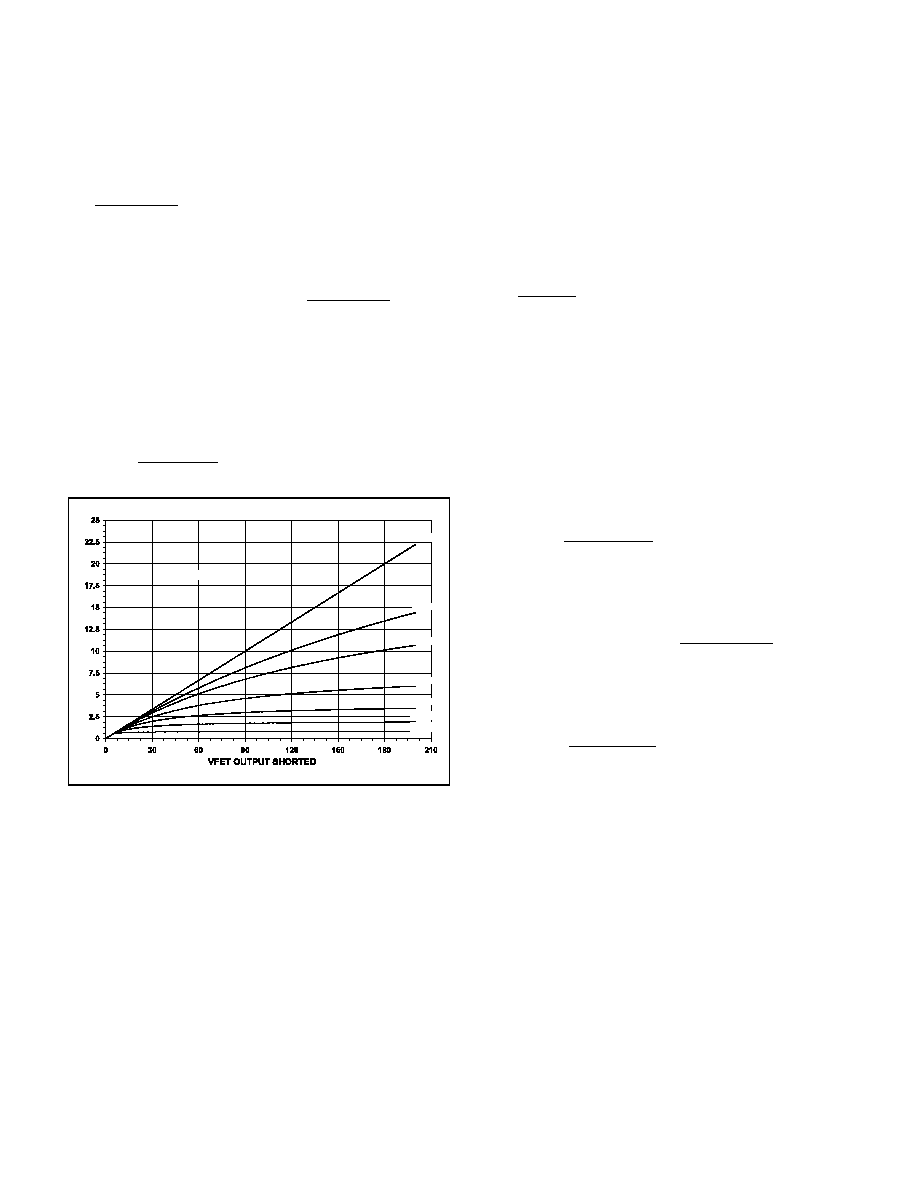
Figure 3. Plot of average power vs. FET voltage
for increasing values of R
PL.
7
UCC1917
UCC2917
UCC3917
CT
I
VIN
I
R
e
CH
MAX
LOAD
t
R
C
LOAD
LOAD
(min)
≠
≠
≠
+
∑
∑
∑
1
∑
R
dt
dV
PL
CT
(4)
Since I
PL
is a function of the output voltage, V
OUT
, which
varies over time, equation 4 must be integrated to solve
for CT(min). However equation 4 can be easily approxi-
mated if the output voltage slews. If the output voltage
slews linearly then the CT charge current contribution
from the power limit circuitry is shown to be at a peak
when V
OUT
= 0V and at 0A when V
OUT
=VIN-V
PL
, where
V
PL
is the power limit voltage threshold. I
PL
is shown in
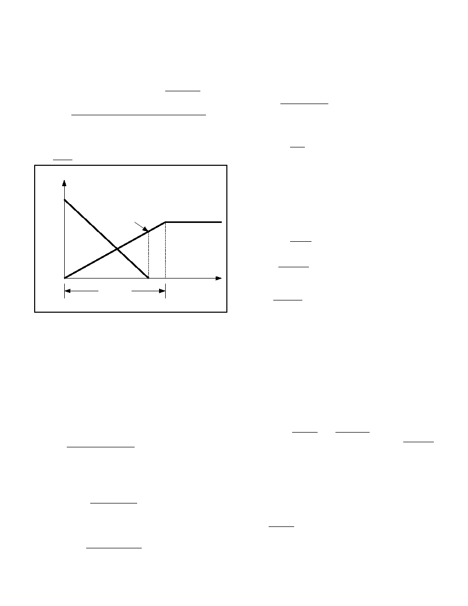
Fig. 4 below.
Where I
PL
is defined as:
(
)
I
VIN
V
V
R
PL
OUT
PL
PL
≠
≠
(5)
The average I
PL
current for the interval (0, T
START
) from
Fig. 4 is defined as:
(
) (
)
I
AVG
VIN
V
R
VIN
PL
PL
PL
∑
∑
≠
2
2
(6)
Equation 4 can now be simplified to:
( )
(
)
CT
I
I
AVG
dV
T
CH
PL
CT
START
min
+
∑
(7)
Please note that the actual on-time in hiccup mode
when operating into a short is defined by:
( )
T on
CT
dV
I
I
pk
CT
CH
PL
(
)
=
∑
+
seconds
(8)
where dV
CT
~2.0V and
( )
I
pk
VIN
R
A
PL
PL
=
(9)
Selecting Other External Components
Other external components are necessary for correct
operation of the IC. Referring to the application diagram
at the back of the data sheet, resistors R
SENSE
, R
SS
,
R1, R2 and R3 are required and follow certain equations
with a brief description following where applicable:
R
=
50mV
I
SENSE
FAULT
(Sense Resistor)
R
=
V
≠ 5V
5mA
SS
IN
(Connected between VSS and
GND)
R3 =
V
10
5mA
IN
≠
(Used in series with a diode to
connect VIN to VDD)
(R1 + R2) > 20k
(Current limit out of VREF)
Lastly, the external capacitors used for the charge pump
are required and need to equal 0.1
µF, i.e. C
IN
= CH =
C1 = C2 = 0.1
µF.
LEVEL Shift Circuitry (Optional)
The UCC3917 can be used in many systems without
logic command or diagnostic feedback. If a system re-
quires control from low-voltage logic or feedback to
low-voltage logic, then level shifting circuits are required.
The level shift circuits in Fig. 5A and Fig. 5B show ways
to interface to LATCH and SHTDWN and the level shift
circuits in Fig. 6 show ways of interfacing from FLTOUT
to low-voltage logic.
In Fig. 5A, resistor R limits the level shift current. Select
R so that the current in the level shift circuit never ex-
ceeds the absolute maximum current in the logic com-
mand inputs, 500
µA. For example, if the maximum
supply voltage for the system is 75V, select
R
V
A
k
>
=
75
500
150
µ
.
R must also be chosen so that the minimum current in
the level shift circuit exceeds the worst case logic
threshold current 60
µA. For example, if the minimum
APPLICATION INFORMATION (cont.)
V
OUT
I
PL
I
PL
(PK)
VIN-V
PL
T
START
Figure 4. Relationship between I
PL
, V
OUT
and T
START
.
8
UCC1917
UCC2917
UCC3917
FLTOUT
R2
R1
LOCAL
VDD
LOCAL
FAULT
13
V
DD
R2
R1
LOCAL
VDD
LOCAL
FAULT
13
V
DD
FLTOUT
11
11
R2
R1
LOCAL
VDD
LOCAL
FAULT
13
V
DD
FLTOUT
11
(A)
(B)
(C)
Figure 6. Potential level shift circuitry to interface to FLTOUT on the UCC3917.
supply voltage for the system is 25V, choose
R
V
A
k
>
=
25
60
416
µ
.
The capacitor C shown on the output of this circuit is
useful to filter the level shift output and prevent false
triggering from noise. The minimum recommended ca-
pacitor value is 100pF. Larger capacitors will result in
better noise immunity and longer delay to logic com-
mand.
The circuit in Fig. 5B accomplished the same function as
the circuit in Fig. 5A, using different components. In this
circuit, select resistor R so that the transistor draws
enough current to exceed the 60
µA logic threshold but
doesn't exceed the 500
µA maximum logic input current.
For example, if the input circuit is 5V logic, then
APPLICATION INFORMATION (cont.)
SHTDWN
OR
LATCH
R
C
VOUT
TO
UCC3917
(A)
C
VOUT
TO
UCC3917
(B)
R
SHTDWN
OR
LATCH
Figure 5. Potential level shift circuitry
to interface to LATCH and SHTDWN on the
UDG-99148
9
UCC1917
UCC2917
UCC3917
Although the UCC3917 is designed to provide system
protection for all fault conditions, all integrated circuits can
ultimately fail short. For this reason, if the UCC3917 is in-
tended for use in safety critical applications where UL or
some other safety rating is required, a redundant safety
device such as a fuse should be placed in series with
the power device. The UCC3917 will prevent the fuse
from blowing for virtually all fault conditions, increasing
system reliability and reducing maintenance cost, in ad-
dition to providing the hot swap benefits of the device.
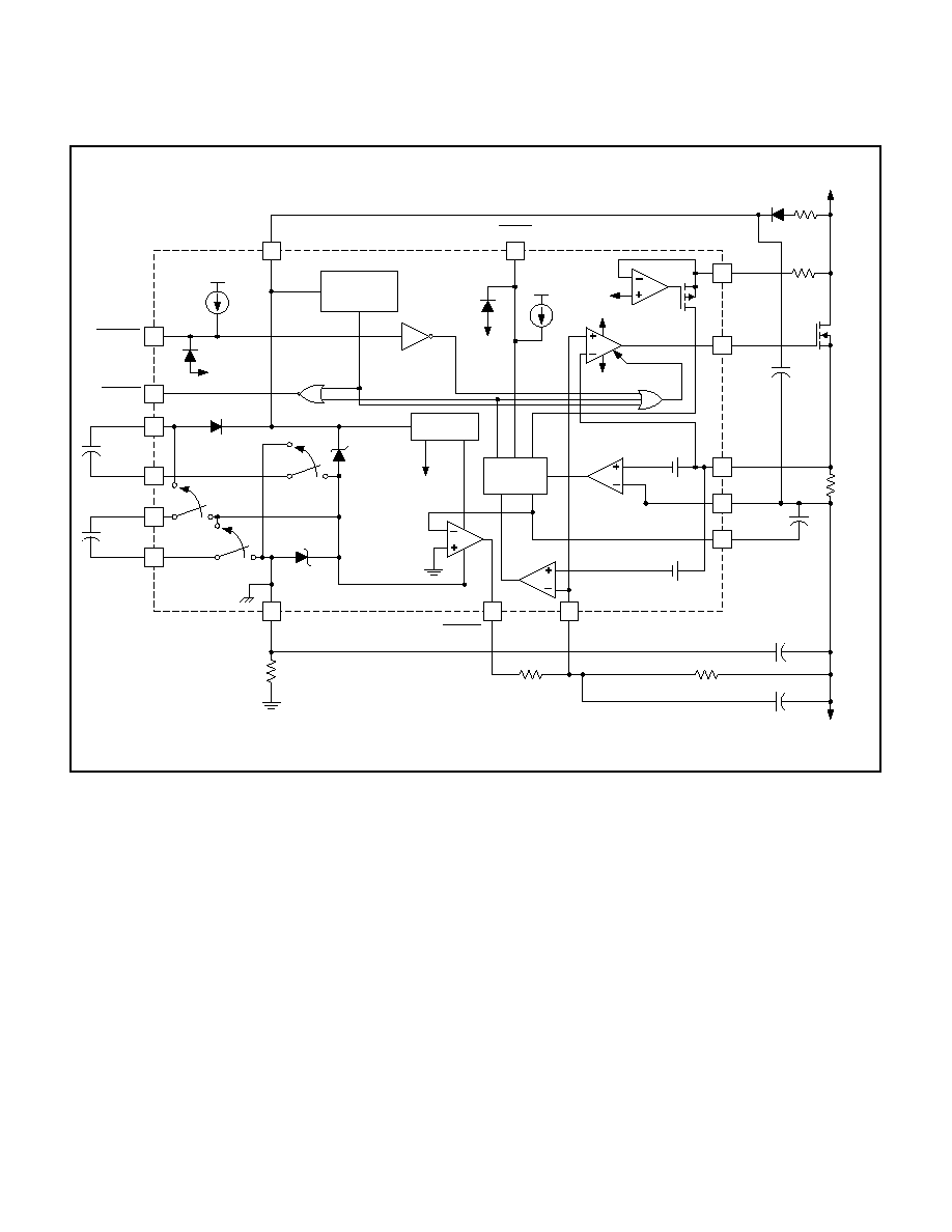
SAFETY RECOMMENDATIONS
UNITRODE CORPORATION
7 CONTINENTAL BLVD. ∑ MERRIMACK, NH 03054
TEL. (603) 424-2410 FAX (603) 424-3460
12
11
8
7
6
5
10
4
2
3
1
13
16
9
14
5V
VOUT
V
DD
VDD
VOUT
DISABLE
OUTPUT
LOW
ON-TIME
DELAY
V
DD
40
µA
VOUT
UVLO
>10V=ENABLE
< 6V=DISABLE
5V
REFERENCE
LOGIC
SUPPLY
10V SHUNT
REGULATOR
SHTDWN
FLTOUT
C1P
C1N
C2P
C2N
VSS
MAXI
CT
VOUT
SENSE
OUTPUT
PLIM
LATCH
VDD
+
200mV
OVER
CURRENT
COMPARATOR
40
µA
C1
C2
R
SS
R1
R2
C
H
C
IN
R3
R
PL
R
SENSE
C
T
D1
V
IN
OUTPUT
+
50mV
15
VREF/CATFLT
C
SS
4V
Figure 7. Positive floating hot swap power manager UCC1917, UCC2917 and UCC3917.
APPLICATION INFORMATION (cont.)
UDG-99056