 | –≠–ª–µ–∫—Ç—Ä–æ–Ω–Ω—ã–π –∫–æ–º–ø–æ–Ω–µ–Ω—Ç: UCC3917N | –°–∫–∞—á–∞—Ç—å:  PDF PDF  ZIP ZIP |

UCC2917, UCC3917
POSITIVE FLOATING HOT SWAP POWER MANAGER
SLUS203B ≠ FEBRUARY 2000 ≠ REVISED AUGUST 2000
1
www.ti.com
D
Manages Hot-Swap of 15 V and Above
D
Precision Fault Threshold
D
Programmable Average Power Limiting
D
Programmable Linear Current Control
D
Programmable Overcurrent Limit
D
Programmable Fault Time
D
Internal Charge Pump to Control External
NMOS Device
D
Fault Output and Catastrophic Fault
Indication
D
Fault Mode Programmable to Latch or Retry
D
Shutdown Control
D
Undervoltage Lockout
description
The UCCx917 family of positive-floating hot-swap managers provides complete power management, hot-swap, and
fault handling capability. The voltage limitation of the application is only restricted by the external component voltage
limitations. The IC provides its own supply voltage via a charge pump referenced to VOUT. The onboard 10-V shunt
regulator protects the IC from excess voltage. The IC also has catastrophic fault indication to alert the user that the
ability to shut off the output NMOS has been bypassed. All control and housekeeping functions are integrated and
externally programmable. These include the fault current level, maximum output sourcing current, maximum fault
time, soft-start time, and average NMOS power limiting.
block diagram
UDG-99055
12
11
8
7
6
5
10
4
2
3
1
13
16
9
15
14
+
≠
5 V
VOUT
VDD
+
≠
VDD
VOUT
DISABLE
OUTPUT
LOW
ON≠TIME
DELAY
VDD
40
µ
A
VOUT
UVLO
>10 V=ENABLE
< 6 V=DISABLE
5 V
REFERENCE
LOGIC
SUPPLY
10 V
5 V
SHTDWN
FLTOUT
C1P
C1N
C2P
C2N
VSS
VREF/CATFLT
MAXI
CT
VOUT
SENSE
OUTPUT
PLIM
LATCH
VDD
+
200 mV
OVER
CURRENT
COMPARATOR
40
µ
A
+
≠
+
≠
+
50 mV
+
≠
4 V
+
Copyright
2000, Texas Instruments Incorporated
PRODUCTION DATA information is current as of publication date.
Products conform to specifications per the terms of Texas Instruments
standard warranty. Production processing does not necessarily include
testing of all parameters.
Please be aware that an important notice concerning availability, standard warranty, and use in critical applications of
Texas Instruments semiconductor products and disclaimers thereto appears at the end of this data sheet.
1
2
3
4
5
6
7
8
16
15
14
13
12
11
10
9
PLIM
SENSE
OUTPUT
VOUT
C2N
C2P
C1N
C1P
LATCH
VREF/CATFLT
MAXI
VDD
SHTDWN
FLTOUT
CT
VSS
D, J, AND N PACKAGE
(TOP VIEW)
UCC2917, UCC3917
POSITIVE FLOATING HOT SWAP POWER MANAGER
SLUS203B ≠ FEBRUARY 2000 ≠ REVISED AUGUST 2000
2
www.ti.com
description (continued)
The fault level across the current-sense amplifier is fixed at 50 mV to minimize total drop out. Once 50 mV is exceeded
across the current-sense resistor, the fault timer starts. The maximum allowable sourcing current is programmed with
a voltage divider from the VREF/CATFLT pin to generate a fixed voltage on the MAXI pin. The current level at which
the output appears as a current source is equal to V
MAXI
divided by the current-sense resistor. If desired, a controlled
current startup can be programmed with a capacitor on MAXI.
When the output current is below the fault level, the output device is switched on with full gate drive. When the output
current exceeds the fault level, but is less than maximum allowable sourcing level programmed by MAXI, the output
remains switched on, and the fault timer starts charging the timing capacitor C
T
. Once C
T
charges to 2.5 V, the output
device is turned off and attempts either a retry sometime later or waits for the state on the LATCH pin to change if
in latch mode. When the output current reaches the maximum sourcing current level, the output device appears as
a current source.
absolute maximum ratings over operating free-air temperature (unless otherwise noted)
Supply current
20 mA
. . . . . . . . . . . . . . . . . . . . . . . . . . . . . . . . . . . . . . . . . . . . . . . . . . . . . . . . . . . . . . . . . . . . . . . . . . . .
SHTDWN current
≠500
µ
A
. . . . . . . . . . . . . . . . . . . . . . . . . . . . . . . . . . . . . . . . . . . . . . . . . . . . . . . . . . . . . . . . . . . . . . .
LATCH current
≠500
µ
A
. . . . . . . . . . . . . . . . . . . . . . . . . . . . . . . . . . . . . . . . . . . . . . . . . . . . . . . . . . . . . . . . . . . . . . . . . .
VREF current
≠500
µ
A
. . . . . . . . . . . . . . . . . . . . . . . . . . . . . . . . . . . . . . . . . . . . . . . . . . . . . . . . . . . . . . . . . . . . . . . . . . .
PLIM current
10 mA
. . . . . . . . . . . . . . . . . . . . . . . . . . . . . . . . . . . . . . . . . . . . . . . . . . . . . . . . . . . . . . . . . . . . . . . . . . . . . .
MAXI input voltage
V
DD
+ 0.3 V
. . . . . . . . . . . . . . . . . . . . . . . . . . . . . . . . . . . . . . . . . . . . . . . . . . . . . . . . . . . . . . . . . .
Junction temperature, T
J
≠55
∞
C to 150
∞
C
. . . . . . . . . . . . . . . . . . . . . . . . . . . . . . . . . . . . . . . . . . . . . . . . . . . . . . . . . .
Storage temperature, T
stg
≠65
∞
C to 150
∞
C
. . . . . . . . . . . . . . . . . . . . . . . . . . . . . . . . . . . . . . . . . . . . . . . . . . . . . . . . .
Lead temperature (Soldering, 10 sec.
)
300
∞
C
. . . . . . . . . . . . . . . . . . . . . . . . . . . . . . . . . . . . . . . . . . . . . . . . . . . . . . .
Stresses beyond those listed under "absolute maximum ratings" may cause permanent damage to the device. These are stress ratings only, and
functional operation of the device at these or any other conditions beyond those indicated under "recommended operating conditions" is not
implied. Exposure to absolute-maximum-rated conditions for extended periods may affect device reliability.
Currents are positive into, negative out of the specified terminal. Consult Packaging Section of the Interface Products Data Book (TI Literature
Number SLUD002) for thermal limitations and considerations of package.
ORDERING INFORMATION
TJ
PACKAGED DEVICES
TJ
DIP (J)
DIP (N)
SOIC (D)
≠40
∞
C to 85
∞
C
UCC2917J
UCC2917N
UCC2917D
0
∞
C to 70
∞
C
UCC3917J
UCC3917N
UCC3917D
electrical characteristics, T
A
= 0
∞
C to 70
∞
C for the UCC3917, ≠40
∞
C to 85
∞
C for the UCC2917,
C
T
= 4.7 nF, T
A
= T
J
, all voltages are with respect to VOUT, current is positive into and negative out
of the specified terminal, (unless otherwise noted)
PARAMETER
TEST CONDITIONS
MIN
TYP
MAX
UNITS
VDD Section
IDD, supply current
From VOUT,
See Note 1
4.0
5
11
mA
UVLO turn on threshold
7.9
8.8
9.7
V
UVLO off voltage
5.5
6.5
7.5
V
VSS regulator voltage
≠6
≠5
≠4
V
NOTE 1: Set by user with RSS.

UCC2917, UCC3917
POSITIVE FLOATING HOT SWAP POWER MANAGER
SLUS203B ≠ FEBRUARY 2000 ≠ REVISED AUGUST 2000
3
www.ti.com
electrical characteristics, T
A
= 0
∞
C to 70
∞
C for the UCC3917, ≠40
∞
C to 85
∞
C for the UCC2917,
C
T
= 4.7 nF, T
A
= T
J
, all voltages are with respect to VOUT, current is positive into and negative out
of the specified terminal, (unless otherwise noted)
PARAMETER
TEST CONDITIONS
MIN
TYP
MAX
UNITS
Fault Timing Section
O erc rrent threshold
TA = 25
∞
C
47.5
50
53
mV
Overcurrent threshold
Over operating temperature
46
50
54
mV
Overcurrent input bias
50
500
nA
CT charge current
VCT = 1 V
≠78
≠50
≠28
µ
A
CT catastrophic fault threshold
3.4
4.5
V
Fault Timing Section (continued)
CT fault threshold
2.25
2.5
2.75
V
CT reset threshold
0.32
0.5
0.62
V
Output duty cycle
Fault condition
1.7%
2.7%
3.7%
Output Section
O tp t high oltage
IOUT = 0
6
8
10
V
Output high voltage
IOUT = ≠100
µ
A
5
7
9
V
O tp t lo
oltage
IOUT = 500
µ
A
0.03
0.50
V
Output low voltage
IOUT = 1 mA
0.6
0.9
V
Linear Current Section
Sense control oltage
MAXI = 100 mV
85
100
115
mV
Sense control voltage
MAXI = 400 mV
370
400
430
mV
Input bias
MAXI = 200 mV
50
500
nA
SHUTDOWN Section
Shutdown threshold
2.0
2.4
2.8
V
Input current
SHTDWN = 0 V
24
40
60
µ
A
Shutdown delay
100
500
ns
LATCH Section
Latch threshold
1.7
2
2.3
V
Input current
LATCH = 0 V
24
40
60
µ
A
FLTOUT Section
Fault output high
VCT = 0 V,
ISOURCE = 0
µ
A
6
8
10
V
Fault output low
VCT = 5 V,
ISINK = 200
µ
A
0.01
0.05
V
Power Limiting Section
VSENSE regulator voltage
IPLIMIT = 64
µ
A
4.5
5
5.5
V
D t c cle control
IPLIMIT = 64
µ
A
0.6%
1.2%
1.7%
Duty cycle control
IPLIMIT = 1 mA
0.045%
0.1%
0.2%
VREF/CATFLT Section
VREF regulator voltage
4.5
5
5.5
V
Fault output low
IVREF/CATFLT = 5 mA
0.22
0.50
V
Output sink current
VCT = 5 V,
VVREF/CATFLT = 5 V
15
40
70
mA
Overload comparator threshold
Relative to MAXI
110
200
290
mV
UCC2917, UCC3917
POSITIVE FLOATING HOT SWAP POWER MANAGER
SLUS203B ≠ FEBRUARY 2000 ≠ REVISED AUGUST 2000
4
www.ti.com
pin assignments
C1N: Negative side of the upper charge-pump capacitor.
C1P: Positive side of the upper charge-pump capacitor.
C2N: Negative side of the lower charge-pump capacitor.
C2P: Positive side of lower charge-pump capacitor.
CT: A capacitor is connected to this pin to set the fault time. The fault time must be more than the time to charge the
external load capacitance (see application information).
FLTOUT: This pin provides fault output indication. Interface to this pin is usually performed through level-shift
transistors. Under a non-fault condition, FLTOUT is pulled to a high state. When a fault is detected by the fault timer
or the undervoltage lockout, this pin is driven to a low state, indicating the output NMOS is in the off state.
LATCH: Pulling this pin low causes a fault to latch until this pin is brought high or a power-on reset is attempted.
However, pulling this pin high before the reset time is reached does not clear the fault until the reset time is reached.
Keeping LATCH high results in normal operation of the fault timer. Users should note there will be an RC delay
dependent upon the external capacitor at this pin.
MAXI: This pin programs the maximum-allowable sourcing current. Since VREF/CATFLT is a regulated voltage, a
voltage divider can be derived to generate the program level for MAXI. The current level at which the output appears
as a current source is equal to the voltage on MAXI divided by the current-sense resistor. If desired, a controlled
current start-up can be programmed with a capacitor on MAXI (to VOUT), and a programmed start delay can be
achieved by driving the shutdown with an open collector/drain device into an RC network.
OUTPUT: Gate drive to the NMOS pass element.
PLIM: This feature ensures that the average external NMOS power dissipation is controlled. A resistor is connected
from this pin to the drain of the external NMOS pass element. When the voltage across the NMOS exceeds 5 V, current
flows into PLIM, which adds to the fault timer charge current, reducing the duty cycle from the 3% level.
SENSE: Input voltage from the current-sense resistor. When there is greater than 50 mV across this pin with respect
to VOUT, a fault is sensed, and C
T
starts to charge.
SHTDWN: This pin provides shutdown control. Interface to this pin is usually performed through level-shift transistors.
When shutdown is driven low, the output disables the NMOS pass device.
VDD: Power to the IC is supplied by an external current-limiting resistor on initial power up or if the load is shorted.
As the load voltages rises (VOUT), a small amount of power is drawn from VOUT by an internal charge pump. The
charge pump's input voltage is regulated by an on-chip 5-V zener. Power to VDD is supplied by the charge pump
under normal operation (i.e., external FET is on).
VOUT: Ground reference for the IC.
VREF/CATFLT: This pin primarily provides an output reference for the programming of MAXI. Secondarily, it provides
catastrophic fault indication. In a catastrophic fault, when the IC unsuccessfully attempts to shutdown the NMOS pass
device, this pin pulls to a low state when C
T
charges above the catastrophic fault threshold. A possible application
for this pin is to trigger the shutdown of an auxiliary FET in series with the main FET for redundancy.
VSS: Negative reference out of the chip. This pin is normally current fed via a resistor to load ground.

UCC2917, UCC3917
POSITIVE FLOATING HOT SWAP POWER MANAGER
SLUS203B ≠ FEBRUARY 2000 ≠ REVISED AUGUST 2000
5
www.ti.com
APPLICATION INFORMATION
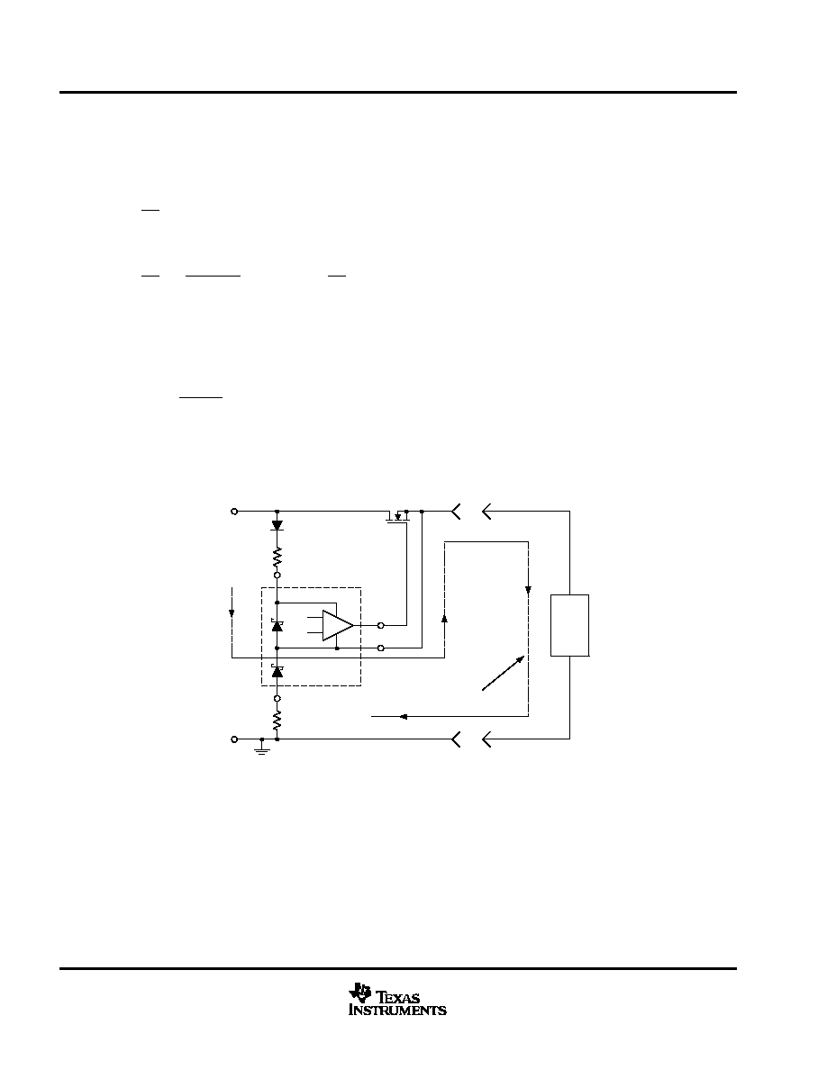
fault timing
Figure 1 shows the detailed circuitry for the fault timing function of the UCC3917. For simplicity, first consider a typical
fault mode where the overload comparator and the current source I3 do not come into play. A typical fault occurs once
the voltage across the current-sense resistor, R
S
, exceeds 50 mV. This causes the overcurrent comparator to trip and
the timing capacitor to charge with current source I1 plus the current from the power limiting amplifier, or PLIM
amplifier. The PLIM amplifier is designed to only source current into the CT pin once the voltage across the output
FET exceeds 5 V. The current I
PL
is related to the voltage across the FET with the following expression:
I
PL
+
V
IN
*
VOUT
*
5 V
R
PL
UDG-00073
S
Q
Q
R
+
≠
+
≠
I3
1 mA
+
≠
2.5 V
0.5 V
I3
50
µ
A
I2
1.5
µ
A
10
+
TO SENSE PIN
TO MAXI PIN
0.2 V
OVERLOAD
COMPARATOR
H = CLOSE
+
≠
+
≠
4
2
1
+
RSENSE
IPL
H = CLOSE
FAULT
LATCH
TO OUTPUT
DRIVE
H = OFF
FAULT COMPARATOR
RESET COMPARATOR
FAULT TIMING CIRCUITRY
VOUT
CT
CT
OVER CURRENT
COMPARATOR
PLIM
AMPLIFIER
PLIM
SENSE
VOUT
50 mV
TO
LOAD
TO
OUTPUT
RPL
VIN
INPUT VOLTAGE
VOUT
5 V
Figure 1. Fault Timing Circuitry for the UCC3917, Including Power Limit and Overload
Note that under normal fault conditions where the output current is just above the fault level, VOUT
V
IN
, I
PL
= 0,
and the C
T
charging current is just I1.
During a fault, C
T
charges at a rate determined by the internal charging current and the external timing capacitor, C
T
.
Once C
T
charges to 2.5 V, the fault comparator switches and sets the fault latch. Setting the fault latch causes both
the output to switch off and the charging switch to open. C
T
must now discharge with current source I2 until 0.5 V is
reached. Once the voltage at C
T
reaches 0.5 V, the fault latch resets (assuming LATCH is high, otherwise the fault
latch does not reset until the LATCH pin is brought high or a power-on reset occurs). This re-enables the output and
allows the fault circuitry to regain control of the charging switch. If a fault is still present, the overcurrent comparator
closes the charging switch causing the cycle to repeat. Under a constant fault the duty cycle is given by:
Duty Cycle
+
I2
I
PL
)
I1
^
1.5
m
A
I
PL
)
50
m
A
where I
PL
is 0
µ
A under normal operations (see Figure 2).

UCC2917, UCC3917
POSITIVE FLOATING HOT SWAP POWER MANAGER
SLUS203B ≠ FEBRUARY 2000 ≠ REVISED AUGUST 2000
6
www.ti.com
APPLICATION INFORMATION
fault timing (continued)
However, under large transients, average power dissipation can be limited using the PLIM pin. A proof follows,
average dissipation in the pass element is given by:
P
FET(avg)
+
V
IN
*
VOUT
I
MAX
Duty Cycle
+
V
IN
*
VOUT
I
MAX
1.5
m
A
I
PL
)
50
m
A
Where (V
IN
≠ VOUT) >>5 V,
I
PL
^
V
IN
*
VOUT
R
PL
OUTPUT
CURRENT
t0
t1 t2
t3
t4
t5
t6 t7 t8
t9t10
VOUT
V
IN
0 V
2.5 V
0.5 V
0 V
t
t
t
I
FAULT
IO(nom)
I
MAX
CT VOLTAGE
(WITH RESPECT TO V OUT)
OUTPUT VOLTAGE
(WITH RESPECT TO GND)
V
CT
IOUT
UDG-99147
Figure 2. Nominal Timing Diagram

UCC2917, UCC3917
POSITIVE FLOATING HOT SWAP POWER MANAGER
SLUS203B ≠ FEBRUARY 2000 ≠ REVISED AUGUST 2000
7
www.ti.com
APPLICATION INFORMATION
fault timing (continued)
t0: Safe condition - output current is nominal, output voltage is at the positive rail, V
IN
.
t1: Fault control reached - output current rises above the programmed fault value, C
T
begins to charge with
50
µ
A.
t2: Maximum current reached - output current reaches the programmed maximum level and becomes a constant
current with value I
MAX
.
t3: Fault occurs - C
T
has charged to 2.5 V, fault output goes low, the FET turns off allowing no output current to flow,
VOUT discharges to ground.
t4: Retry - C
T
has discharged to 0.5 V, but fault current is still exceeded, C
T
begins charging again, FET is on, VOUT
rises to V
IN
.
t5 = t3: Illustrates 3% duty cycle.
t6 = t4:
t7: Output short circuit - if VOUT is short circuited to ground, C
T
charges at a higher rate depending upon the values
for V
IN
and R
PL
.
t8: Fault occurs - output is still short circuited, but the occurrence of a fault turns the FET off so no current is conducted.
t9: Output short circuit released, still in fault mode.
t10 = t0: Fault released, safe condition - return to normal operation of the circuit breaker.
Note that t6 ≠ t5
36
◊
(t5 ≠ t4).
and where I
PL
>> 50
µ
A, the duty cycle can be approximated as:
1.5
m
A
R
PL
V
IN
*
VOUT
Therefore the average power dissipation in the MOSFET can be approximated by:
P
FET(avg)
+
V
IN
*
VOUT
I
MAX
1.5
m
A
R
PL
V
IN
*
VOUT
+
I
MAX
1.5
m
A
R
PL
Notice that since (V
IN
≠ VOUT) cancels, average power dissipation is limited in the NMOS pass element (see Figure
3). Also, a value for R
PL
can be roughly determined from this approximation.
R
PL
+
P
FET(avg)
I
MAX
1.5
m
A

UCC2917, UCC3917
POSITIVE FLOATING HOT SWAP POWER MANAGER
SLUS203B ≠ FEBRUARY 2000 ≠ REVISED AUGUST 2000
8
www.ti.com
APPLICATION INFORMATION
fault timing (continued)
AVERAGE POWER vs FET VOLTAGE
P
A
VG - A
verage Power - W
VDS - FET Voltage (output Shorted) - V
0
30
60
90
120
150
180
210
0
2.5
5.0
7.5
10.0
12.5
15.0
17.5
20.0
22.5
25.0
IMAX = 4 A
RPL =
RPL = 10 M
RPL = 5 M
RPL = 2 M
RPL = 1 M
RPL = 500 k
RPL = 200 k
Figure 3.
overload comparator
The overload comparator provides protection against a shorted load during normal operation when the external
N-channel FET is fully enhanced. Once the FET is fully enhanced the linear current amplifier essentially saturates
and the system is in effect operating open loop. Once the FET is fully enhanced the linear current amplifier requires
a finite amount of time to respond to a shorted output possibly destroying the external FET. The overload comparator
is provided to quickly shutdown the external MOSFET in the case of a shorted output (if the FET is fully enhanced).
During an output short, C
T
is charged by I3 at
1 mA. The current threshold for the overload comparator is a function
of I
MAX
and a fixed offset and is defined as:
I
OVERLOAD
+
I
MAX
)
200 mV R
S
Once the overcurrent comparator trips, the UCC3917 enters a programmed fault mode (hiccup or latched). It should
be noted that on subsequent retries during hiccup mode or if a short should occur when the UCC3917 is actively
limiting the current, the output current will not exceed I
MAX
. In the event that the external FET does not respond during
a fault the UCC3917 will set the VREF/CATFLT pin low to indicate a catastrophic failure.
UCC2917, UCC3917
POSITIVE FLOATING HOT SWAP POWER MANAGER
SLUS203B ≠ FEBRUARY 2000 ≠ REVISED AUGUST 2000
9
www.ti.com
APPLICATION INFORMATION
selecting the minimum timing capacitance
To ensure that the IC starts up correctly the designer must ensure that the fault time programmed by C
T
exceeds the
startup time of the load. The startup time (t
START
) is a function of several components; load resistance and load
capacitance, soft-start components R1, R2 and C
SS
, the power limit current contribution determined by R
PL
, and C
IN
.
For a parallel capacitor-constant current load:
t
START
+
C
LOAD
VIN
I
MAX
*
I
LOAD
For a parallel R-C load:
t
START
+
R
LOAD
C
LOAD
n 1
*
V
IN
I
MAX
R
LOAD
If the power limit function is not be used then C
T(min)
can be easily found:
C
T(min)
+
I
CH
t
START
dV
CT
where dV
CT
is the hysteresis on the fault detection circuitry. During operation in the latched fault mode configuration
dV
CT
= 2.5 V. When the UCC3917 is configured for the hiccup or retry mode of fault operation dV
CT
= 2.0 V.
If the power limit function is used, the C
T
charging current becomes a function of I
CH
+ I
PL
. C
T(min)
is found by
integrating equation 4 with respect to V
CT
.
C
T(min)
^
I
CH
)
VIN
*
I
MAX
R
LOAD
1
*
e
*
t
R
LOAD
C
LOAD
R
PL
dt
dV
CT
The minimum timing capacitance is found to be:
C
T(min)
+
1
R
PL
dV
CT
I
CH
R
PL
)
V
IN
*
I
MAX
R
LOAD
t
START
)
V
IN
R
LOAD
C
LOAD
(1)
(2)
(3)
(4)
(5)
UCC2917, UCC3917
POSITIVE FLOATING HOT SWAP POWER MANAGER
SLUS203B ≠ FEBRUARY 2000 ≠ REVISED AUGUST 2000
10
www.ti.com
APPLICATION INFORMATION
selecting other external components
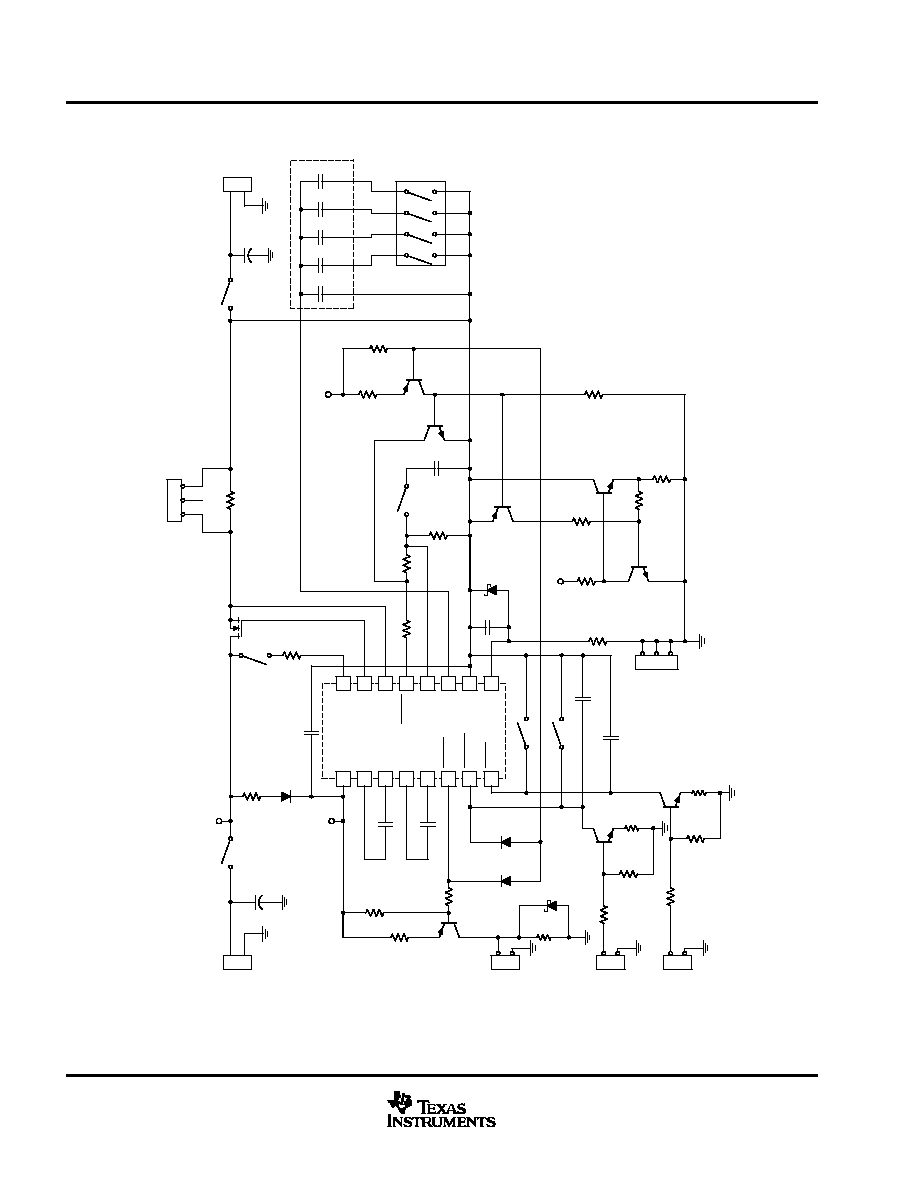
Other external components are necessary for correct operation of the IC. Referring to Figure 11, resistors R
SENSE
,
R
SS
, R
DD
, R17, R18, and R19 and the following equations apply:
R
SENSE
+
50 mV
I
FAULT
R
SS
+
V
IN
*
5 V
I
DD
R
DD
+
V
IN
*
10
I
DD
(R17 + R18 + R19) > 20 k
(Current limit out of VREF)
Lastly, use 0.1
µ
F for the external charge pump capacitors.
soft start
The soft-start circuits in Figure 4a and 4b gradually ramp up the load current on power-up, retry, or if the SHTDWN
pin is pulled high. Control circuitry (not shown) turns on Q1 to discharge C1 when FLTOUT or SHTDWN are low (i.e.,
external power MOSFET is off) so the load current always ramps from zero. The circuit in Figure 4a uses an
inexpensive bipolar transistor for Q1 so the component cost is lower than the circuit in Figure 4b.
R3
R2
R1
C1
+
Q1
VREF
15
14
MAXI
4
VOUT
(a)
R2
R1
C1
+
VREF
15
14
MAXI
4
VOUT
Q1
(b)
UDG-00017
Figure 4. Soft≠start Circuits
Soft start minimizes the voltage disturbance on the power bus when a circuit card is inserted into a live back plane.
This disturbance could reset a system, which is not desirable when high availability is required. A server is an example
of a high availability system.

UCC2917, UCC3917
POSITIVE FLOATING HOT SWAP POWER MANAGER
SLUS203B ≠ FEBRUARY 2000 ≠ REVISED AUGUST 2000
11
www.ti.com
APPLICATION INFORMATION
soft start (continued)
Soft start is initiated with the SHTDWN pin in Figure 5. The anode of D2 is grounded when the card is in the back
plane. R2 limits the SHTDWN pin current to between 60
µ
A and 500
µ
A (i.e., 60
µ
A < 0.65 V / R2 < 500
µ
A).
UDG-00019
U1
UCC3917
13 VDD
8
C1P
7
C1N
6
C2P
5
C2N
11
FLOUT
12 SHTDWN
16 LATCH
1
PLIM
3
OUTPUT
2
SENSE
15
VREF/CATFLT
14
MAXI
10
CT
4
VOUT
9
VSS
D2
RDD
R1
Q1
D1
R2
D2
RGR
Z
BACK PLANE
PLUG≠IN CARD
VIN
GND
SHORT PIN
Figure 5. Soft Starting with SHTDWN
I/O interface
The UCC3917's SHTDWN and LATCH inputs and FLTOUT output are referenced to VOUT. Level-shifting circuits are
needed if the UCC3917 communicates with logic that is referenced to load/system ground.
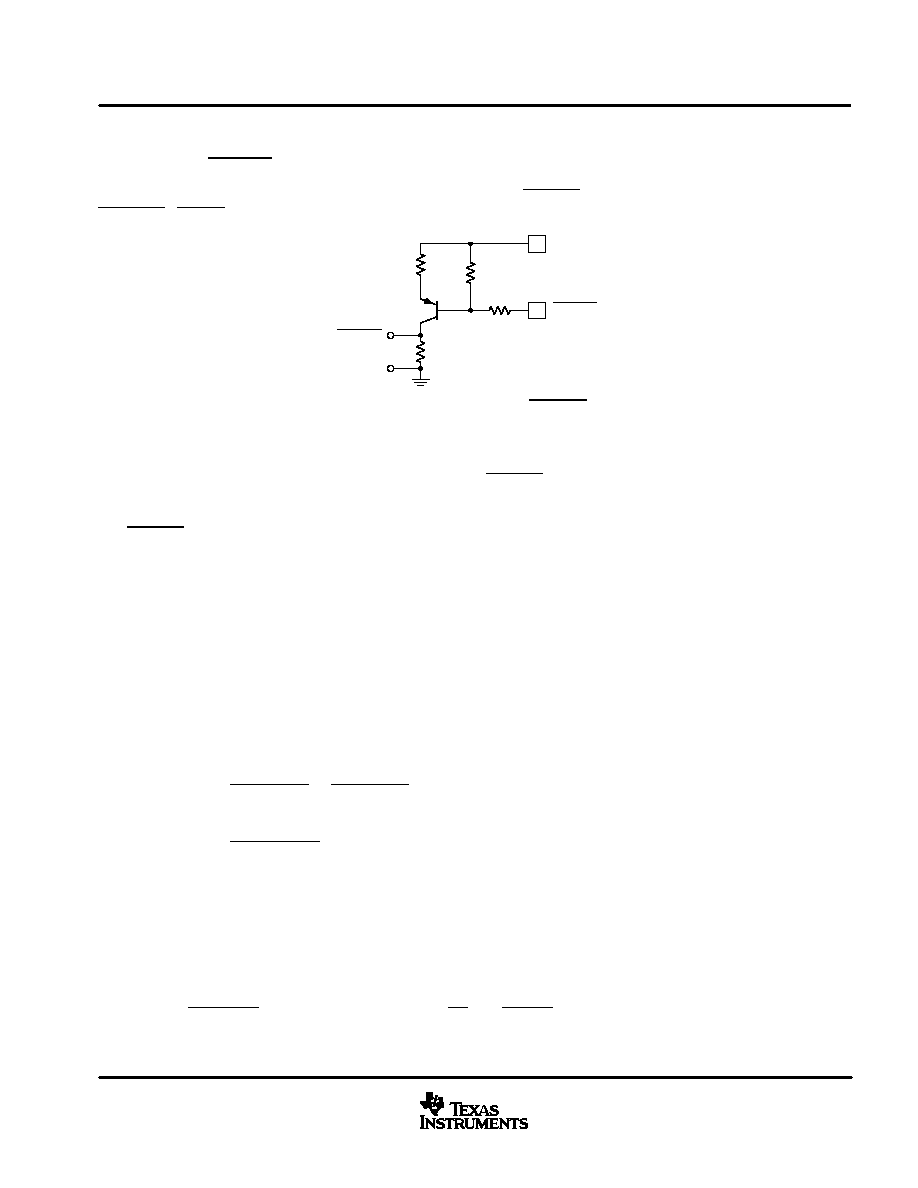
interfacing to LATCH and SHTDWN
Two level shift circuits for LATCH and SHTDWN are shown in Figure 6. The optocoupler (Figure 6a) is simple, but
the constant-current sink (Figure 6b) is low cost.
IN
R1
GND
Q1
R2
(b)
(b). CONSTANT≠CURRENT SINK INTERFACE
SHTDWN / LATCH
R3
IN
1 k
GND
4N25
SHTDWN / LATCH
VOUT
4
(a). OPTOCOUPLER INTERFACE
UDG-00020
Figure 6. Interfaces

UCC2917, UCC3917
POSITIVE FLOATING HOT SWAP POWER MANAGER
SLUS203B ≠ FEBRUARY 2000 ≠ REVISED AUGUST 2000
12
www.ti.com
APPLICATION INFORMATION
example #1:
A TTL signal controls the LATCH input of the UCC3917 using the circuit in Figure 6b. Determine the component values
if the maximum load voltage is 60 V.
solution:
The assumptions for this analysis are:
V
BE
0.65 V, V
CE(sat)
0.1 V, and R1 // R2 << hfe
◊
R3.
Voltage measurements are with respect to load ground.
Select Q1. The LATCH input is internally pulled up to the charge pump voltage, which is 10 V above the load voltage.
Q1 is therefore subjected to 70 V in a 60 V system. A FMMTA06 transistor, with a V
CEO(max)
of 80 V, is suitable for
Q1 in this application.
determine R1-R3.
The interface circuit responds to a TTL input as follows:
Logic "0" input: 0 V < V
IL
< 0.8 V
0
µ
A < I
C
< 60
µ
A and V
C
> 1.7 V
Logic "1" input: 2 V < V
IH
< 5 V
60
µ
A < I
C
< 500
µ
A and V
C
< 1.7 V
This response establishes the relationship between R1, R2, and R3.
If V
IN
= V
IL(max)
= 0.8 V then:
(a) Q1 is off
V
B
V
IL(max)
◊
R2 / (R1+R2) < V
BE
R1 / R2 > 0.23
If V
IN
= V
IH(max)
= 5 V, then:
(a) I
C
= (1.7 V ≠ V
CE(sat)
) / R3 < 500
µ
A
R3 > 3.2 k
, and
(b) V
C
= (V
CE(sat)
+ V
E
) < 1.7 V
V
E
< 1.6 V, and
(c) V
E
= (V
B
≠ V
BE
) < 1.6 V
V
B
< 2.25 V, and
(d) V
B
V
IH (max)
)
◊
R2 / (R1+R2) < 2.25 V
R1 / R2 > 1.222
If V
IN
= V
IH(min)
= 2 V, then:
(a) V
B
= V
IH(min)
◊
R2 / (R1+R2)
V
B
= 2 V / (1+R1 / R2)
(b) I
C
= (V
B
≠ V
BE
) / R3 > 60
µ
A
R3 < (V
B
≠ V
BE
) / 60
µ
A
In summary, R1, R2, and R3 obey the inequalities:
R1 / R2 > 1.222, and
3.2 k
< R3 < (V
B
≠ 0.65) / 60
µ
A, where V
B
= 2 V / (1+R1 / R2)
If R1 / R2 = 1.3, then 3.2 k
< R3 < 3.66 k
. R1 = 4.64 k
for the case where R2 = R3 = 3 k
.
The same design can be used to control the UCC3917's SHTDWN input.
UCC2917, UCC3917
POSITIVE FLOATING HOT SWAP POWER MANAGER
SLUS203B ≠ FEBRUARY 2000 ≠ REVISED AUGUST 2000
13
www.ti.com
APPLICATION INFORMATION
interfacing to FLTOUT
The level shift circuit in Figure 7 is a way to interface to FLTOUT. The operation of this circuit and the
SHTDWN / LATCH level shift circuit in Figure 6b are similar.
R3
GND
Q1
R2
FLTOUT
R4
R1
13 VDD
11 FLTOUT
UDG-00022
Figure 7. Interfacing to FLTOUT
example:
Problem: Design a TTL compatible output level shifter for FLTOUT. The maximum system voltage is 60 V.
Solution: Use the level shift circuit in Figure 7.
The FLTOUT output can swing to the charge pump voltage, which is 10 V above the load voltage. In a 60 V application,
the collector-emitter of Q1 can be as high as ≠70 V. A FMMT593 transistor, with a V
CEO(max)
rating of ≠100 V, is a
suitable choice for Q1.
1. Output saturation voltage constraint.
V
C(on)
= V
E
+ V
CE(sat)
> 2.4 V (i.e. TTL output high)
If V
C(on)
= 2.6 V, then V
E
= (2.6 V + (≠0.1 V)) = 2.5 V.
2. Source current constraint.
I
C
= 100
µ
A
3. Calculate the value of R3.
R3
+
6 V
*
V
E
I
E
^
6 V
*
V
E
I
C
R3
+
(6 V
*
2.5 V)
100
m
A
+
35 k
4. Calculate the base voltage.
V
B
= V
E
+ V
BE
V
B
= (2.5 V ≠ 0.65 V) = 1.85 V
5. The voltage divider formula for R1 and R2 is:
R2
(R1
)
R2)
6 V
^
6 V
*
V
B
or
R1
R2
+
6 V
V
B
*
1
UCC2917, UCC3917
POSITIVE FLOATING HOT SWAP POWER MANAGER
SLUS203B ≠ FEBRUARY 2000 ≠ REVISED AUGUST 2000
14
www.ti.com
APPLICATION INFORMATION
example: (continued)
This equation assumes negligible loading by Q1. That is:
R1
R2
¶¶
hfe
R3
If hfe = 100, then:
R1
R2
+
6
1.85
*
1
+
2.24 and R1
R2
¶¶
(100
35 K)
+
3.5 M
If R2 = R3 = 34.8 k
, then R1 = 15.4 k
6. The output voltage is set by R4.
I
C
R4
u
2.4 V
R4
ß
2.4 V
100
m
A
+
24 k
W
.
Choose R4
+
49.9 k
W
preloading the output
R
DD
provides a sneak path for 3mA≠11mA of current (e.g., @ 0 V output) to trickle into the load when the power FET
is off (see Figure 8).
UDG-00021
VIR
RDD
VDD
+
≠
10V
5V
VSS
OUTPUT
VOUT
UCC3917
RSS
GND
LOAD
SNEAK PATH
GND
VO
Figure 8. Simplified Schematic Illustrating I
DD
Sneak Path
This current causes an unacceptably high output voltage at shutdown if the output is not adequately loaded. In this
case, it is necessary to preload the HSPM output to keep the shutdown voltage level acceptable. The preload also
insures reliable start-up of the UCC3917 by holding the output voltage low when power is first applied to the HSPM.
A resistor is usually an unacceptable preload because it creates a power dissipation problem when the FET turns
on. For example, a 90.9-
preload (used to limit the shutdown voltage of a 48-V HSPM to less than 1 V) adds 25-W
of power dissipation to the system. In a 100-V system, this dissipation increases to 110 W. The power dissipation
overhead increases with the system voltage squared for a resistive preload.
UCC2917, UCC3917
POSITIVE FLOATING HOT SWAP POWER MANAGER
SLUS203B ≠ FEBRUARY 2000 ≠ REVISED AUGUST 2000
15
www.ti.com
APPLICATION INFORMATION
preloading the output (continued)
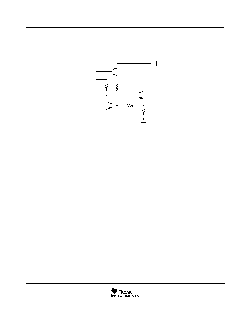
The active load in Figure 9 limits the shutdown voltage without creating a power dissipation problem.
Q3
4
VOUT
Q1
R1
R2
R3
R4
TAPER ≠
VIN
Q2
UDG-00024
Figure 9. Active Preload
This load is a constant-current sink (i.e., Q3 is off) when the power FET is off. The shutdown voltage is less than 0.85
V if the sink current, set by R1, is greater than 11 mA:
I
SINK(FEToff)
[
V
BE
R1
ß
11 mA
The power dissipation of Q1 is kept to a minimum when the power FET turns on by tapering the sink current as the
load voltage rises:
I
SINK(FETon)
[
V
BE
R1
*
V
O
R2
(R1
R3)
For R1 << R2 << R3
Control circuitry turns on Q3 to activate current tapering. Tapering the current causes the power dissipation of Q1 to
peak when the load voltage is:
V
O
+
V
BE
2
R3
R2
The power dissipated by Q1 at this voltage is:
P
D(max)Q1
+
V
BE
2
2
R3
(R1
R2)
In the case of a brownout or if the input voltage rises slowly (e.g., adjustable lab power supply), it is possible for Q1
to dwell in the maximum power dissipation region for a significant time. Limiting the power dissipation of Q1 below
its maximum rating insures reliable operation in this case.
UCC2917, UCC3917
POSITIVE FLOATING HOT SWAP POWER MANAGER
SLUS203B ≠ FEBRUARY 2000 ≠ REVISED AUGUST 2000
16
www.ti.com
APPLICATION INFORMATION
example:
Problem: Design a 14-mA active preload for a 60-V HSPM.
Solution: Set the sink current:
R1
+
V
BE
I
SINK(FEToff)
+
0.65 V
14 mA
+
46.4
W
Use a BC846B transistor for Q1. This device has a collector breakdown voltage of 65 V and power dissipation rating
of 225 mW.
Select R2 & R3 to limit the power dissipation of Q1 to less than 225 mW, say 150 mW:
R3
R2
+
2
V
BE
2
R1
P
D(max)Q1
R3
R2
+
2
0.65 V
2
46.4
W
0.15 W
R3
R2
+
65.9
If R2 = 3.01 k
, then R3 = 198 k
.
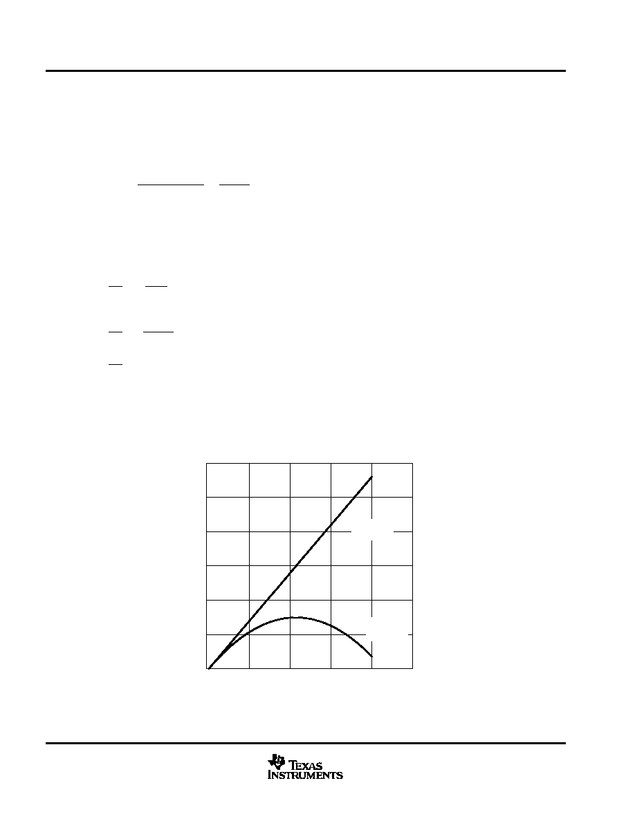
The power dissipation of Q1 is shown in Figure 10.
POWER DISSIPATION
vs
OUTPUT VOLTAGE
VO - Output Voltage - V
P
D
- Power Dissipation - W
0
10
20
30
40
50
0
0.1
0.2
0.3
0.4
0.5
0.6
Constant
Current
Tapered
Current
Figure 10.

UCC2917, UCC3917
POSITIVE FLOATING HOT SWAP POWER MANAGER
SLUS203B ≠ FEBRUARY 2000 ≠ REVISED AUGUST 2000
17
www.ti.com
APPLICATION INFORMATION
protecting the 5-V regulator
The UCC3917's 5-V regulator can overvoltage if VOUT is loaded with less than 11 mA (min) on power up. The
overvoltage mechanism is best understood by recognizing that the 5-V Zener diode in the UCC3917 block diagram,
is actually a feedback shunt regulator. This regulator turns on when the voltage across the UCC3917's 10-V Zener
diode is greater than the UVLO threshold. If VOUT is unloaded and power is applied to the UCC3917, the UVLO
threshold cannot be reached and the 5-V regulator impedance is infinite.
Consequently, the entire input voltage appears across the shunt regulator causing it to break down. Clamping its
voltage with Zener diode to 5.6 V can protect the regulator. The Zener diode is unnecessary if the current drawn from
VOUT is greater than 11 mA when power is initially applied to the UCC3917.
evaluation circuit example
A 28 V to 60 V @ 1-A HSPM evaluation circuit is shown in Figure 11. Level translation circuitry allows communications
with logic referenced to load ground. This circuit is available as a DV3917 Evaluation Board. Contact your local Texas
Instruments sales representative for more information.
safety recommendations
Although the UCC3917 is designed to provide system protection for all fault conditions, all integrated circuits can
ultimately fail short. For this reason, if the UCC3917 is intended for use in safety critical applications where UL or some
other safety rating is required, a redundant safety device such as a fuse should be placed in series with the power
device. The UCC3917 prevents the fuse from blowing for virtually all fault conditions, increasing system reliability and
reducing maintenance cost, in addition to providing the hot-swap benefits of the device.
UCC2917, UCC3917
POSITIVE FLOATING HOT SWAP POWER MANAGER
SLUS203B ≠ FEBRUARY 2000 ≠ REVISED AUGUST 2000
18
www.ti.com
APPLICATION INFORMATION
SHUTDOWN
13
7
8
6
11
5
16
12
1
2
3
15
10
14
9
4
C7 0.1
µ
F
C8 0.1
µ
F
VDD
C1P
C1N
C2P
C2N
FL
T
OUT
SHTDWN
LA
TCH
PLIM
OUTPUT
SENSE
VREF/CA
TFL
T
MAXI
CT
VOUT
VSS
0.1
µ
F
V
DD
D1
1N4148
Rdd
4.7 k
1 W
R23
200 k
V
IN
Q1
IRF530S
C1
4.7
µ
F
100 V
J1
+
≠
IN
2
1
C13 0.01
µ
F
C14 0.01
µ
F
D3
1N4148
D2
1N4148
R3
15.4 k
R2
34.8 k
Q2
FMMT593
R1
34.8 k
P1
+
≠
F
AUL
T
1
2
R4
49.9 k
*D4
BZX04C4V3ZX
4.3 V
Q3
FMMT
A06
R7
3.57 k
R6
3.57 k
Q4
FMMT
A06
R10
3.57 k
R9
3.57 k
R5
7.32 k
R8
7.32 k
P3
+
≠
REMOTE
LA
TCH
1
2
P2
+
≠
REMOTE
SHUTDOW
SHUTDOW
1
2
R17 49.9 k
Rss
5.6 k
1 W
C9
0.1
µ
F
D5
BZX84C5V6
5.6 V
R19
2 k
R13
200 k
Q5
MMBT5809
Q6
FMMT593
R21
1 M
R20
15CK
V
DD
R16
1 M
TP1
GND
1
2
3
Q7
MMBT5039
R12
200 k
V
IN
Q8
BC346B
R14
3.01 k
R15
47
TP2
CS
12
3
Rsense 0.5
1 W 2%
+
≠
C10
4.7
µ
F
100 V
+
J2
+
≠
OUT
2
1
C2
C3
C4
C5
C6
SS
1
2
3
4
5
67
8
C2
≠
C6 0.22
µ
F
U1
UCC3917
R18
49.9 k
10
µ
F
10 V
Q5
FMMT593
S6
S1
S2
S3
S4
S7
UDG-00025
C
IN
C
SS
Figure 11. A 28 V to 60 V @ 1-A Positive Floating HSPM Evaluation Circuit Using the UCC3917

IMPORTANT NOTICE
Texas Instruments Incorporated and its subsidiaries (TI) reserve the right to make corrections, modifications,
enhancements, improvements, and other changes to its products and services at any time and to discontinue
any product or service without notice. Customers should obtain the latest relevant information before placing
orders and should verify that such information is current and complete. All products are sold subject to TI's terms
and conditions of sale supplied at the time of order acknowledgment.
TI warrants performance of its hardware products to the specifications applicable at the time of sale in
accordance with TI's standard warranty. Testing and other quality control techniques are used to the extent TI
deems necessary to support this warranty. Except where mandated by government requirements, testing of all
parameters of each product is not necessarily performed.
TI assumes no liability for applications assistance or customer product design. Customers are responsible for
their products and applications using TI components. To minimize the risks associated with customer products
and applications, customers should provide adequate design and operating safeguards.
TI does not warrant or represent that any license, either express or implied, is granted under any TI patent right,
copyright, mask work right, or other TI intellectual property right relating to any combination, machine, or process
in which TI products or services are used. Information published by TI regarding third≠party products or services
does not constitute a license from TI to use such products or services or a warranty or endorsement thereof.
Use of such information may require a license from a third party under the patents or other intellectual property
of the third party, or a license from TI under the patents or other intellectual property of TI.
Reproduction of information in TI data books or data sheets is permissible only if reproduction is without
alteration and is accompanied by all associated warranties, conditions, limitations, and notices. Reproduction
of this information with alteration is an unfair and deceptive business practice. TI is not responsible or liable for
such altered documentation.
Resale of TI products or services with statements different from or beyond the parameters stated by TI for that
product or service voids all express and any implied warranties for the associated TI product or service and
is an unfair and deceptive business practice. TI is not responsible or liable for any such statements.
Mailing Address:
Texas Instruments
Post Office Box 655303
Dallas, Texas 75265
Copyright
2002, Texas Instruments Incorporated