 | –≠–ª–µ–∫—Ç—Ä–æ–Ω–Ω—ã–π –∫–æ–º–ø–æ–Ω–µ–Ω—Ç: UCC3918DP | –°–∫–∞—á–∞—Ç—å:  PDF PDF  ZIP ZIP |
UCC3918
LOW ON RESISTANCE HOT SWAP POWER MANAGER
SLUS384B ≠ NOVEMBER 1999 ≠ REVISED JUNE 2000
1
www.ti.com
D
Integrated 0.075-
Power MOSFET
D
3 V to 6 V Operation
D
External Analog Control of Fault Current
from 0 A to 4 A
D
Independent Analog Control of Current
Limit Up to 5 A
D
Fast Overload Protection
D
Unidirectional Switch
D
Minimal External Components
D
1-
µ
A I
CC
When Disabled
D
Programmable On Time
D
Programmable Start Delay
D
Fixed 3% Duty Cycle
description
The UCC3918 low on-resistance hot swap power manager provides complete power management, hot swap
capability, and circuit breaker functions. The only components needed to operate the device, other than supply
bypassing, are a timing capacitor, and two programming resistors. All control and housekeeping functions are
integrated, and externally programmable. These include the fault current level, maximum output sourcing
current, maximum fault time, and startup delay. In the event of a constant fault, the internal fixed 3% duty cycle
ratio limits the average output power. The IFAULT pin allows linear programming of the fault level current from
0 A to 4 A.
Fast overload protection is accomplished by an additional overload comparator. Its threshold is internally set
above the maximum sourcing current limit setting. In the event of a short circuit or extreme current condition,
this comparator is tripped, shutting down the output. This function is needed since the maximum sourcing
current limit loop has a finite bandwidth.
When the output current is below the fault level, the output MOSFET is switched on with a nominal resistance
of 0.075
. When the output current exceeds the fault level or the maximum sourcing level, the output remains
on, but the fault timer starts charging a capacitor connected to the CT pin (C
T
). Once C
T
charges to a preset
threshold, the switch is turned off, and remains off for 30 times the programmed fault time. When the output
current reaches the maximum sourcing level, the MOSFET transitions from a switch to a constant current
source.
The UCC3918 is designed for unidirectional current flow, emulating an ideal diode in series with the power
switch. This feature is particularly attractive in applications where many devices are powering a common bus,
such as with SCSI termintation power (Termpwr). The UCC3918 can also be put into the sleep mode, drawing
only 1
µ
A of supply current.
Other features include an open-drain fault output indicator, thermal shutdown, undervoltage lockout, 3 V to 6 V
operation, and a low thermal resistance small-outline power package.
Copyright
2000, Texas Instruments Incorporated
PRODUCTION DATA information is current as of publication date.
Products conform to specifications per the terms of Texas Instruments
standard warranty. Production processing does not necessarily include
testing of all parameters.
Please be aware that an important notice concerning availability, standard warranty, and use in critical applications of
Texas Instruments semiconductor products and disclaimers thereto appears at the end of this data sheet.
Pin 5 serves as the lowest impedance to the electrical
ground. Pins 4, 12, and 13, serve as heat sink/ground.
These pins should be connected to large etch PCB areas
to help dissipate heat.
1
2
3
4
5
6
7
8
16
15
14
13
12
11
10
9
VIN
VIN
VIN
GND*
GND*
FAULT
SHTDWN
IFAULT
VOUT
VOUT
VOUT
GND*
GND*
NC
CT
IMAX
DP PACKAGE
(TOP VIEW)
UCC3918
LOW ON RESISTANCE HOT SWAP POWER MANAGER
SLUS384B ≠ NOVEMBER 1999 ≠ REVISED JUNE 2000
2
www.ti.com
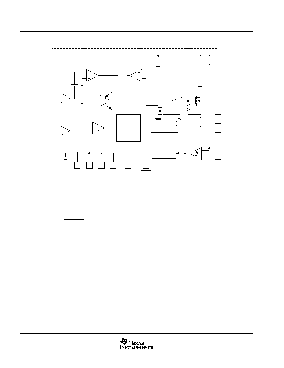
functional block diagram
9
8
5
4
13
12
10
6
7
3
2
1
INTERNAL
BIAS
THERMAL
SHUTDOWN
ON TIME
CONTROL
3% DUTY
CYCLE
CHARGE
PUMP
16
15
14
VIN
VIN
VIN
VOUT
VOUT
VOUT
SHTDWN
FAULT
CT
HEAT SINK GND
PINS
GND
IFAULT
IMAX
CURRENT
FAULT LEVEL
OVERLOAD
COMPARATOR
OVERCURRENT
COMPARATOR
REVERSE
COMPARATOR
V
OUT
+
20mV
CURRENT SENSE
1.5V
H = OPEN
MAXIMUM
CURRENT
LEVEL
+
+
+
+
+
+
UDG≠99153
absolute maximum ratings over operating free-air temperature (unless otherwise noted)
}
Input Voltage
8 V
. . . . . . . . . . . . . . . . . . . . . . . . . . . . . . . . . . . . . . . . . . . . . . . . . . . . . . . . . . . . . . . . . . . . . . . . . . . . . . . .
SOIC Power dissipation
2.5 W
. . . . . . . . . . . . . . . . . . . . . . . . . . . . . . . . . . . . . . . . . . . . . . . . . . . . . . . . . . . . . . . . . . . .
Fault output sink current
50 mA
. . . . . . . . . . . . . . . . . . . . . . . . . . . . . . . . . . . . . . . . . . . . . . . . . . . . . . . . . . . . . . . . . . .
Fault output voltage
VIN
. . . . . . . . . . . . . . . . . . . . . . . . . . . . . . . . . . . . . . . . . . . . . . . . . . . . . . . . . . . . . . . . . . . . . . . . . .
Output Current (dc)
Internally Limited
. . . . . . . . . . . . . . . . . . . . . . . . . . . . . . . . . . . . . . . . . . . . . . . . . . . . . . . . . . . . . .
Input Voltage SHTDWN, IFAULT, IMAX
≠0.3 V to VIN
. . . . . . . . . . . . . . . . . . . . . . . . . . . . . . . . . . . . . . . . . . . . . .
Storage temperature range T
stg
≠65
_
C to 150
_
C
. . . . . . . . . . . . . . . . . . . . . . . . . . . . . . . . . . . . . . . . . . . . . . . . . . . .
Operating virtual junction temperature T
J
≠55
_
C to 150
_
C
. . . . . . . . . . . . . . . . . . . . . . . . . . . . . . . . . . . . . . . . . . .
Lead temperature (soldering, 10 seconds)
300
_
C
. . . . . . . . . . . . . . . . . . . . . . . . . . . . . . . . . . . . . . . . . . . . . . . . . . .
Stresses beyond those listed under "absolute maximum ratings" may cause permanent damage to the device. These are stress ratings only, and
functional operation of the device at these or any other conditions beyond those indicated under "recommended operating conditions" is not
implied. Exposure to absolute-maximum-rated conditions for extended periods may affect device reliability.
Unless otherwise indicated, voltages are reference to ground and currents are positive into, negative out of the specified terminal. Pulsed is
defined as a less than 10% duty cycle with a maximum duration of 500
µ
s. Consult Packaging Section of Databook for thermal limitations and
considerations of package.

UCC3918
LOW ON RESISTANCE HOT SWAP POWER MANAGER
SLUS384B ≠ NOVEMBER 1999 ≠ REVISED JUNE 2000
3
www.ti.com
electrical characteristics at T
A
= 0
∞
C to 70
∞
C, VIN = 5 V, R
IMAX
= 42.2 k
, R
IFAULT
= 52.3 k
,
SHTDWN = 2.4 V, T
A
= T
J
(unless otherwise noted)
PARAMETER
TEST CONDITIONS
MIN
TYP
MAX
UNITS
Supply Section
Voltage input range, VIN
3
5
6
V
VDD supply current
No load
1
2
mA
Sleep mode current
SHTDWN = 0.2 V
0.5
5
µ
A
Output Section
IOUT = 1 A to 4 A,
VIN = 5 V,
TA = 25
∞
C
0.075
0.095
R
IOUT = 1 A to 4 A,
VIN = 3 V,
TA = 25
∞
C
0.09
0.116
RDS(on)
IOUT = 1 A to 4 A,
VIN = 5 V
0.075
0.125
IOUT = 1A to 4A,
VIN = 3 V
0.09
0.154
Reverse leakage current
SHTDWN = 0 V,
VIN = 0 V
VOUT = 5 V
20
µ
A
Initial startup time
See Note 1
100
µ
s
Thermal shutdown
VIN = 5 V,
See Note 1
170
_
C
Thermal hysteresis
See Note 1
10
_
C
Output leakage
SHTDWN = 0.2 V,
VOUT = 0 V
20
µ
A
RIFAULT = 105 k
0.75
1
1.25
A
Trip current
RIFAULT = 52.3 k
1.7
2
2.3
A
Trip current
RIFAULT = 34.8 k
2.5
3
3.5
A
RIFAULT = 25.5 k
3.3
4
4.7
A
RIMAX = 118 k
0.3
1
1.7
A
RIMAX = 60.4 k
1
2
3
A
Maximum output current
RIMAX = 42.2 k
2
3
4
A
Maximum out ut current
RIMAX = 33.2 k
2.5
3.8
5.1
A
RIMAX = 27.4 k
3.0
4.6
6.2
A
Fault Section
CT charge current
VCT = 1 V
≠50
≠36
≠22
µ
A
CT discharge current
VCT = 1 V
0.5
1.2
2.0
µ
A
Output duty cycle
VOUT = 0 V
1.5
3
6
%
CT fault threshold
0.8
1.3
1.8
V
CT reset threshold
0.25
0.5
0.75
V
Shutdown Section
Shutdown threshold
1.1
1.5
2.0
V
Shutdown hysteresis
100
mV
Input low current
SHTDWN = 0V
≠500
0
500
nA
Input high current
SHTDWN = 2V
≠2
≠1
≠0.5
µ
A
Open Drain Fault Output Section
High level output current
1
µ
A
Low level output voltage
IOUT = 1mA
0.4
0.9
V
NOTE 1: Ensured by design. Not production tested.
UCC3918
LOW ON RESISTANCE HOT SWAP POWER MANAGER
SLUS384B ≠ NOVEMBER 1999 ≠ REVISED JUNE 2000
4
www.ti.com
pin descriptions
CT: A capacitor connected to this pin sets the maximum fault time. The maximum time must be greater than
the time to charge external load capacitance. The nominal fault time is defined as:
T
FAULT
+
22.2
103
C
T
Once the fault time is reached the output shuts down for a time given by:
T
SD
+
0.667
106
C
T
This equates to a 3% duty cycle. The recommended minimum value for the C
T
capacitor is 0.1
µ
F.
FAULT: Open-drain output, which pulls low on any condition that causes the output to open; Fault, Thermal
Shutdown, Shutdown, and maximum sourcing current greater than the fault time.
GND: This is the most negative voltage in the circuit. All 4 ground pins should be used, and properly heat sunk
on the PCB.
IFAULT: A resistor connected from this pin to ground sets the fault threshold. The resistor versus fault current
is set by the formula
R
FAULT
+
105 k
W
I
TRIP
IMAX: A resistor connected from this pin to ground sets the maximum sourcing current. The resistor vs the
output sourcing current is set by the formula:
R
IMAX
+
126 k
W
Maximum Sourcing Current
SHTDWN: When this pin is brought low, the IC is put into sleep mode. The input threshold is hysteretic, allowing
the user to program a startup delay with an external RC circuit.
VIN: This is the input voltage to the UCC3918. The recommended operating voltage range is 3V to 6V. All VIN
pins should be connected together and to the power source.
VOUT: Output voltage for the circuit breaker. When switched the output voltage will be approximately:
V
OUT
+
V
IN
*
0.075
W
I
OUT
.
All VOUT pins should be connected together and to the load.
(1)
(2)
(3)
(4)
(5)
UCC3918
LOW ON RESISTANCE HOT SWAP POWER MANAGER
SLUS384B ≠ NOVEMBER 1999 ≠ REVISED JUNE 2000
5
www.ti.com
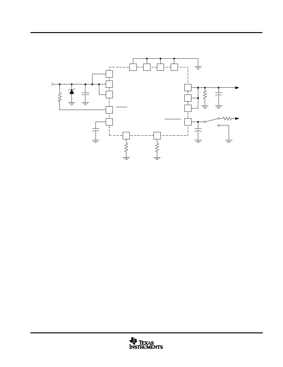
APPLICATION INFORMATION
9
8
5
4
13
12
10
6
7
3
2
1
16
15
14
VIN
VIN
VIN
VOUT
VOUT
VOUT
SHTDWN
FAULT
CT
HEAT SINK GND
PINS
GND
IFAULT
IMAX
R
IMAX
R
IFAULT
C
T
C
SD
R
SD
V
IN
S6
R
L
C
OUT
V
OUT
C
IN
D1
R1
V
IN
UDG≠99152
Figure 1. Typical Application
protecting the UCC3918 from voltage transients
The parasitic inductance associated with the power distribution can cause a voltage spike at V
IN
if the load
current is suddenly interrupted by the UCC3918. It is important to limit the peak of this spike to less than 6 V
to prevent damage to the UCC3918. This voltage spike can be minimized by:
∑
Reducing the power distribution inductance (e.g., twist the positive "+" and negative "≠" leads of the
power supply feeding V
IN
, locate the power supply close to the UCC3918 or use a PCB ground plane).
∑
Decoupling V
IN
with a capacitor, C
IN
(refer to Figure 1), located close to the VIN pin. This capacitor is
typically less than 1
µ
F to limit the inrush current.
∑
Clamping the voltage at V
IN
below 6 V with a Zener diode, D1 (refer to Figure 1), located close to the VIN
pin.
estimating maximum load capacitance
For circuit breaker applications, the rate at which the total output capacitance can be charged depends on the
maximum output current available and the nature of the load. For a constant-current current-limited circuit
breaker, the output comes up if the load requires less than the maximum available short-circuit current.
To ensure recovery of a duty-cycle of the current-limited circuit breaker from a short-circuited load condition,
there is a maximum total output capacitance that can be charged for a given unit ON time (fault time). The design
value of ON or fault time can be adjusted by changing the timing capacitor C
T
.

UCC3918
LOW ON RESISTANCE HOT SWAP POWER MANAGER
SLUS384B ≠ NOVEMBER 1999 ≠ REVISED JUNE 2000
6
www.ti.com
APPLICATION INFORMATION
estimating maximum load capacitance
For worst-case constant-current load of value just less than the trip limit; C
OUT(max)
can be estimated from:
C
OUT(max)
+
I
MAX
*
I
LOAD
22
103
C
T
V
OUT
Where V
OUT
is the output voltage and I
MAX
is the maximum sourcing current.
For a resistive load of value R
LOAD
, the value of C
OUT(max)
can be estimated from:
C
OUT(max)
+
22
103
C
T
R
LOAD
n
1
1
*
VOUT
I
MAX
R
LOAD
UDG≠97071
Figure 2. Load Curent, Timing Capacitor Voltage and Output Voltage of the UCC3918 Under Fault
(6)
(7)
UCC3918
LOW ON RESISTANCE HOT SWAP POWER MANAGER
SLUS384B ≠ NOVEMBER 1999 ≠ REVISED JUNE 2000
7
www.ti.com
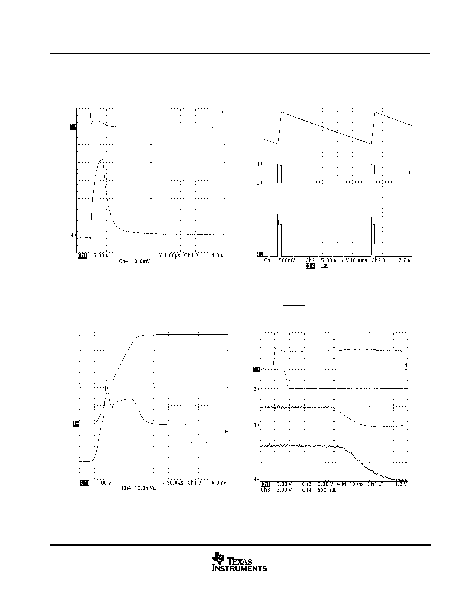
TYPICAL CHARACTERISTICS
Figure 3
REVERSE VOLTAGE COMPARATOR
RESPONSE TIME
VIN
0 A
1 A
2 A
3 A
4 A
C
OUT
= 22 F
R
LOAD
= 5
C
IN
= 5 F
R
IFAULT
= 52.3 k
R
IMAX
= 42.0 k
I
IN
Figure 4
FAULT TIMING WAVEFORMS
V
OUT
= 0 V
R
LOAD
= SHORT
C
IN
= 5 F
R
IFAULT
= 52.3 k
R
IMAX
= 42.2 k
OUTPUT CURRENT
C
T
(0.1 F)
FAULT OUT
Figure 5
INRUSH CURRENT LIMITING
V
OUT
I
INPUT
@ 0.5 A/DIV
0 V
0 A
C
OUT
= 22 F
R
LOAD
= 5
C
IN
= 5 F
R
IFAULT
= 52.3 k
R
IMAX
= 60.4 k
Figure 6
FAULT AND OUTPUT TURN-OFF
DELAY FROM CT FAULT
THRESHOLD
C
OUT
= 0 F
R
LOAD
= 5
C
IN
= 5 F
C
T
= OPEN
R
IFAULT
= 52.3 k
R
IMAX
= 42.4 k
FAULT OUT
C
T
VOUT
I
OUT
(R
LOAD
= 5 )
UCC3918
LOW ON RESISTANCE HOT SWAP POWER MANAGER
SLUS384B ≠ NOVEMBER 1999 ≠ REVISED JUNE 2000
8
www.ti.com
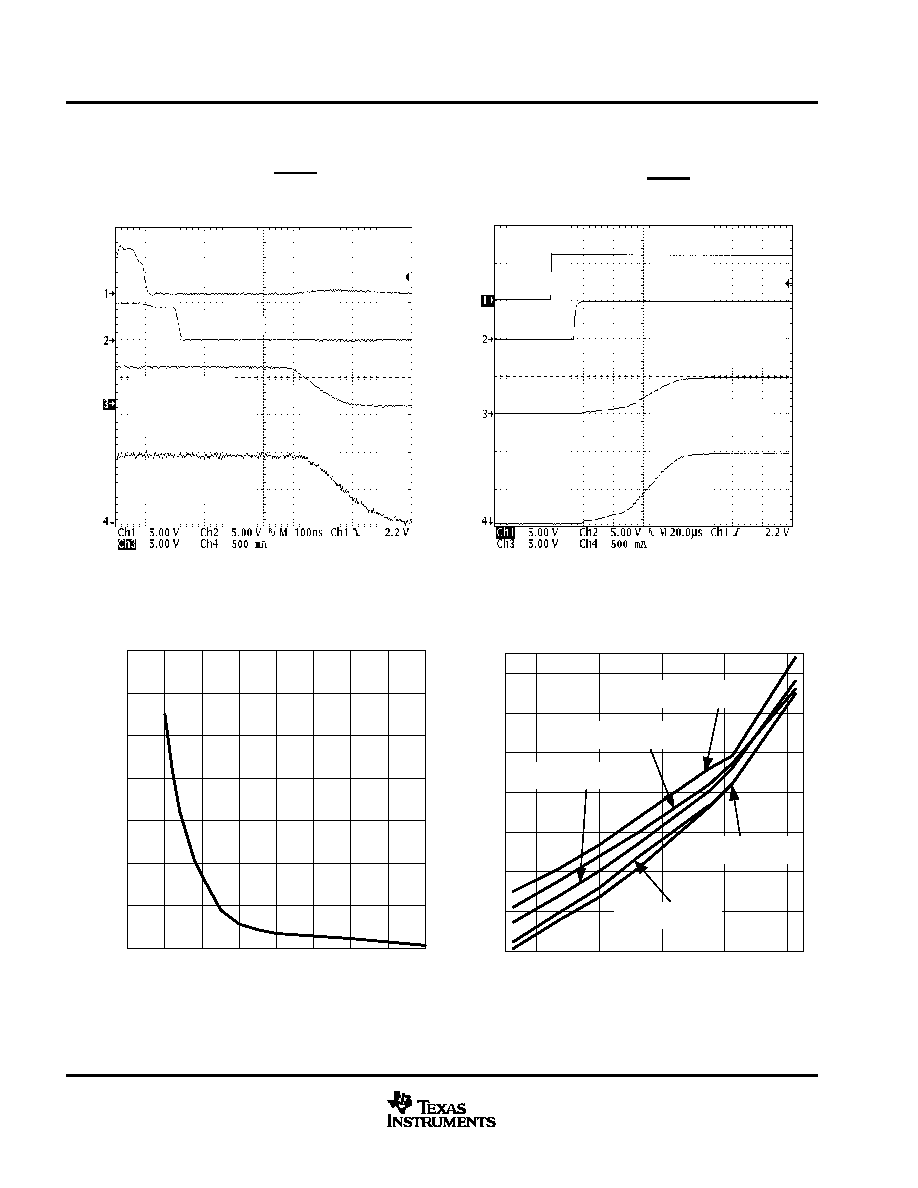
TYPICAL CHARACTERISTICS
SHUTDOWN
FAULT OUT
VOUT
I
OUT
Figure 7
PROPAGATION DELAY
SHUTDOWN TO FAULT AND
OUTPUT RAMP-DOWN
C
OUT
= 0 F
R
LOAD
= 5
C
IN
= 5 F
R
IFAULT
= 52.3 k
R
IMAX
= 42.4 k
Figure 8
PROPAGATION DELAY
ENABLE TO FAULT AND
OUTPUT RAMP-UP
0 A
1 A
SHUTDOWN
FAULT OUT
VOUT
I
OUT
(R
LOAD
= 5 )
C
OUT
= 0 F
R
LOAD
= 5
C
IN
= 5 F
R
IFAULT
= 52.3 k
R
IMAX
= 42.4 k
Figure 9
ON-STATE RESISTANCE
vs
OUTPUT CURRENT
R
DS(on)
On≠State Resistance ≠ m
0.5
0
1.5
1.0
2.5
2.0
3.5
3.0
4.0
55
65
75
85
95
105
115
125
I
OUT
≠ Output Current ≠ A
Figure 10
ON-STATE RESISTANCE
vs
TEMPERATURE
T
A
≠ Free-Air Temperature ≠
_
C
R
DS(on)
On≠State Resistance ≠ m
80
VIN = 3 V, I = 1 A
VIN = 5 V, I = 1 A
Average
VIN = 3 V, I = 4 A
VIN = 5 V, I = 4 A
≠ 40
40
0
120
40
60
80
100
50
70
90
110
UCC3918
LOW ON RESISTANCE HOT SWAP POWER MANAGER
SLUS384B ≠ NOVEMBER 1999 ≠ REVISED JUNE 2000
9
www.ti.com
APPLICATION INFORMATION
safety considerations
Although the UCC3918 is designed to provide system protection for all fault conditions, all integrated circuits
can ultimately fail short. For this reason, if the UCC3918 is intended for use in safety critical applications where
UL
or some other safety rating is required, a redundant safety device such as a fuse should be placed in series
with the power device. The UCC3918 prevents the fuse from blowing for virtually all fault conditions, increasing
system reliability and reducing maintenance cost, in addition to providing the hot swap benefits of the device.

IMPORTANT NOTICE
Texas Instruments Incorporated and its subsidiaries (TI) reserve the right to make corrections, modifications,
enhancements, improvements, and other changes to its products and services at any time and to discontinue
any product or service without notice. Customers should obtain the latest relevant information before placing
orders and should verify that such information is current and complete. All products are sold subject to TI's terms
and conditions of sale supplied at the time of order acknowledgment.
TI warrants performance of its hardware products to the specifications applicable at the time of sale in
accordance with TI's standard warranty. Testing and other quality control techniques are used to the extent TI
deems necessary to support this warranty. Except where mandated by government requirements, testing of all
parameters of each product is not necessarily performed.
TI assumes no liability for applications assistance or customer product design. Customers are responsible for
their products and applications using TI components. To minimize the risks associated with customer products
and applications, customers should provide adequate design and operating safeguards.
TI does not warrant or represent that any license, either express or implied, is granted under any TI patent right,
copyright, mask work right, or other TI intellectual property right relating to any combination, machine, or process
in which TI products or services are used. Information published by TI regarding third≠party products or services
does not constitute a license from TI to use such products or services or a warranty or endorsement thereof.
Use of such information may require a license from a third party under the patents or other intellectual property
of the third party, or a license from TI under the patents or other intellectual property of TI.
Reproduction of information in TI data books or data sheets is permissible only if reproduction is without
alteration and is accompanied by all associated warranties, conditions, limitations, and notices. Reproduction
of this information with alteration is an unfair and deceptive business practice. TI is not responsible or liable for
such altered documentation.
Resale of TI products or services with statements different from or beyond the parameters stated by TI for that
product or service voids all express and any implied warranties for the associated TI product or service and
is an unfair and deceptive business practice. TI is not responsible or liable for any such statements.
Mailing Address:
Texas Instruments
Post Office Box 655303
Dallas, Texas 75265
Copyright
2001, Texas Instruments Incorporated