 | –≠–ª–µ–∫—Ç—Ä–æ–Ω–Ω—ã–π –∫–æ–º–ø–æ–Ω–µ–Ω—Ç: UCC3920 | –°–∫–∞—á–∞—Ç—å:  PDF PDF  ZIP ZIP |
4/97
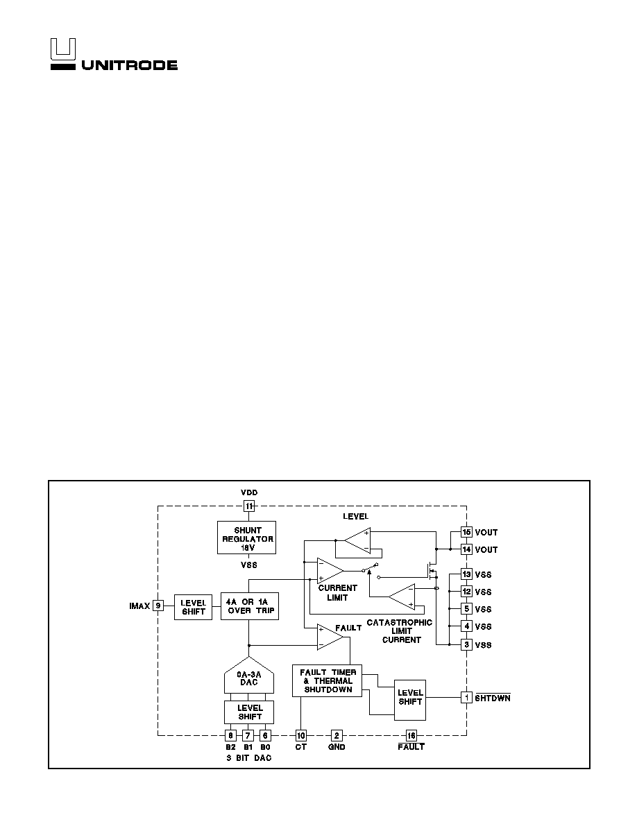
BLOCK DIAGRAM
∑
Integrated 0.1
Power MOSFET
∑
≠3V to ≠15V Operation
∑
Programmable
Electronic Circuit
Breaker
∑
Digital Programmable
Current Limit from 0A
to 3A
∑
Programmable
Maximum Output
Current from 0A to 4A
∑
Programmable On
Time
∑
Fixed 2% Fault Duty
Cycle
∑
Thermal Shutdown
∑
Fault Output Indicator
∑
Power SOIC Package
≠3V to ≠15V Hot Swap Power Manager
FEATURES
DESCRIPTION
UCC2920
UCC3920
PRELIMINARY
UDG-96235-1
The UCC3920 Low RDSon Hot Swap Power Manager provides complete power man-
agement, hot swap capability, and circuit breaker functions. The only component
needed to operate the device, other than supply bypassing, is the fault timing capaci-
tor, CT. All control and housekeeping functions are integrated and externally program-
mable. These include the fault current level, maximum output sourcing current, maxi-
mum fault time, and start up delay. In the event of a constant fault, the internal fixed
2% duty cycle ratio limits the average output power.
The internal 3 bit DAC allows programming of the fault level current from 0mA to
500mA with 250mA resolution, and from 500mA to 3A with 500mA resolution. The
IMAX control pin sets the maximum sourcing current to 1A above the fault level when
driven low, and to a full 4A when driven high for applications which require fast output
charging.
When the output current is below the fault level, the output MOSFET is switched on
with a nominal resistance of 0.1
. When the output current exceeds the fault level or
the maximum sourcing level, the output remains on, but the fault timer starts charging
CT. Once CT charges to a preset threshold, the switch is turned off, and remains off
for 50 times the programmed fault time. When the output current reaches the maxi-
mum sourcing level, the MOSFET transitions form a switch to a constant current
source, regulating the output current at a constant level.
Other features include an Open Drain Fault Output Indicator, Thermal Shutdown, Un-
dervoltage Lockout, ≠3V to ≠15V operation, and a low thermal resistance Small Out-
line Power Package. All level shifting is done internally, which means that the DAC,
IMAX and Shutdown Inputs can be driven form the logic supply. The fault output is
also referenced to the logic GND, so this can easily interface back to the logic supply.
UCC2920
UCC3920
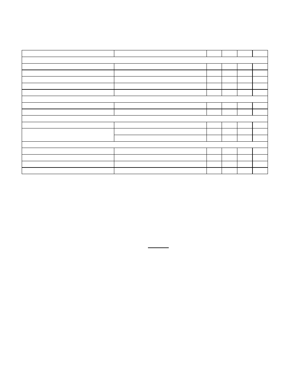
PARAMETER
TEST CONDITIONS
MIN
TYP
MAX
UNITS
Supply Section
Voltage Input Range - VDD
Minimum < VDD < Maximum (Note 3)
3
5
5.5
V
Voltage Input Range - VSS
Minimum < VSS < Maximum
≠13.2
≠12
≠3
V
VSS Supply Current
0.5
2
mA
VDD Supply Current
0.5
2
mA
Sleep Mode Current
Shutdown = 0.2V
0.5
2
mA
Shunt Clamp Voltage - (VDD - VSS)
I = 2mA to 10mA, Note 3
16.2
18
20
V
Output Section
Voltage Drop
I
OUT
= 1A
0.1
0.2
V
I
OUT
= 2A
0.2
0.4
V
I
OUT
= 3A
0.3
0.6
V
I
OUT
= 1A, VSS = ≠3V
0.1
0.2
V
I
OUT
= 2A, VSS = ≠3V
0.2
0.4
V
I
OUT
= 3A, VSS = ≠3V
0.3
0.6
V
Short Circuit Response
Note 1
20
µ
S
DAC Section
Trip Current
Code = 000
0
20
µ
A
Code = 001
0.1
0.25
0.45
A
Code = 010
0.25
0.5
0.75
A
Code = 011
0.75
1
1.25
A
Code = 100
1.25
1.5
1.75
A
Code = 101
1.7
2
2.3
A
Code = 110
2.1
2.5
2.9
A
Code = 111
2.5
3
3.5
A
Maximum Output Current
Code = 000, IMAX = 0.4V
0
20
µ
A
Code = 011, IMAX = 0.4V
1
2
3
A
Code = 101, IMAX = 0.4V
2
3
4
A
Code = 111, IMAX = 0.4V
2.8
4
5.2
A
IMAX = 2.4V, All Codes
3
4
5.2
A
ELECTRICAL CHARACTERISTICS
Unless otherwise stated, these specificaiton apply for T
A
= 0∞C to 70∞C for the
UCC3920 and T
A
= ≠40∞C to 85∞C for the UCC2920, T
A
= T
J
.
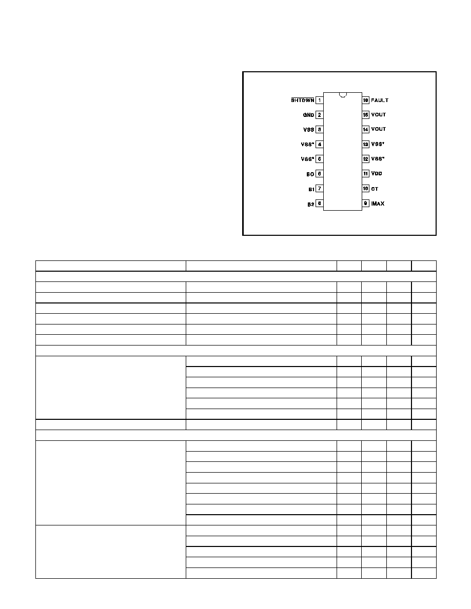
CONNECTION DIAGRAM
DIL-16, SOIC-16 (Top View)
N, DP Package
ABSOLUTE MAXIMUM RATINGS
Input Supply Voltage
(VDD). . . . . . . . . . . . . . . . . . . . . . . . . . . . . . . . . . . . . . . . +7V
(VSS) . . . . . . . . . . . . . . . . . . . . . . . . . . . . . . . . . . . . . . . ≠15V
Maximum Differential Suppy (VDD - VSS). . . . . . . . . . . . . . 18V
Maximum Supply Shunt Current . . . . . . . . . . . . . . . . . . . 20mA
Fault Output Sink Current. . . . . . . . . . . . . . . . . . . . . . . . . 20mA
Fault Output Voltage. . . . . . . . . . . . . . . . . . . . . . . . . . . . . . . . 7V
Output Current (DC) . . . . . . . . . . . . . . . . . . . . Internally Limited
TTL Input Voltage . . . . . . . . . . . . . . . . . . . . . . . . . . . . -0.3 to 7V
Storage Temperature . . . . . . . . . . . . . . . . . . .
-
65∞C to +150∞C
Junction Temperature . . . . . . . . . . . . . . . . . . ≠55∞C to +150∞C
Lead Temperature (Soldering, 10 sec.) . . . . . . . . . . . . . +300∞C
Currents are positive into, negative out of the specified terminal.
Pulsed is defined as a less than 10% duty cycle with a maximum
duration of 500
µ
S. Consult Packaging Section of Databook for
thermal limitations and considerations of packages.
Note: Do Not Connect to GND. * Heat sink connection points -
electronically connected to Vss.
For N Package, pins 4, 12, and 13 are N/C.
2
PARAMETER
TEST CONDITIONS
MIN
TYP
MAX
UNITS
Fault Section
CT Charge Current
V
CT
= 1V, Note 2
≠50
≠36
≠22
µ
A
CT Discharge Current
V
CT
= 1V, Note 2
0.36
0.6
1
µ
A
Output Duty Cycle
VOUT = 0V
1
2
4
%
CT Fault Threshold
Note 2
1.25
1.5
1.75
V
CT Reset Threshold
Note 2
0.25
0.5
0.75
V
Shutdown Section
Shutdown Threshold
1.1
1.5
1.9
V
Shutdown Hysterisis
50
mV
Open Drain Fault Output
High Level Output Current
1
µ
A
Low Level Output Voltage
IOUT = 2mA
0.4
V
IOUT = 10mA
0.9
V
Logic Input DC Characteristics
Input Voltage High
2
V
Input Voltage Low
0.8
V
Input High Current
VIH = 2.4V
3
10
µ
A
Input Low Current
VIL = 0.4V
1
µ
A
ELECTRICAL CHARACTERISTICS (cont.)
Unless otherwise stated, these specificaiton apply for T
A
= 0∞C to 70∞C for
the UCC3920 and T
A
= ≠40∞C to 85∞C for the UCC2920, T
A
= T
J
.
UCC2920
UCC3920
PIN DESCRIPTIONS
BO - B2: These pins provide a digital input to the DAC.
They can be used to provide a digital soft start, adaptive
current limiting, or be strapped for static applications.
CT: A capacitor connected to CT sets the maximum fault
time. The maximum must be more than the time to charge
external load capacitance. The maximum fault time is
defined as T
FAULT
= 28
∑
10
3
∑
CT. Once the fault time is
reached the output will shutdown for a time given by: TSD
= 1.67
∑
10
6
∑
CT, this equates to a 2% duty cycle.
FAULT: Open drain output which, pulls low, from VDD to
GND, upon any condition which causes the output to
open: Fault, Thermal Shutdown, or Shutdown.
GND: Reference return for VDD and VSS (VIN). This
serves as the reference point for digital signals.
IMAX: When this pin is at a logic low the linear output
current will always be 1A above the programmed trip
level, and with a logic high the linear current will always
be a constant 4A for applications which require fast
charging of load capacitance.
SHTDWN: When this pin is brought down low the IC is
put into a sleep mode.
VDD: Positive input voltage to the circuit breaker. The
input voltage range is 3V to 5.5V. If the total voltage
excursion, VDD - VSS could be 15V or greater, VDD
should have an external limiting resistor in series with it.
VSS: The input voltage to the circuit breaker. The
recommended voltage range is ≠3.3V to ≠15V.
VOUT: Output voltage for the circuit breaker. When
switched the output voltage will be approximately VIN +
0.1
∑
IOUT.
Note 1: Guaranteed by design. Not 100% tested in production.
Note 2: Voltages measured with respect to VSS.
Note 3: An external resistor in series with VDD could be used to limit the current to 10mA if an input voltage higher than 15V is de-
sired.
3
UCC2920
UCC3920
TYPICAL APPLICATION
UDG-96237
Note 1: Most applications will require a capacitor mounted between VOUT and GND at the IC pins to cancel out stray inductance.
Estimating Maximum Load Capacitance
For power management applications, the rate at which
the total output capacitance can be charged depends
on the maximum output current available and the na-
ture of the load. For a constant-current current-limited
circuit, the output will rise if the load asks for less than
the maximum available short-circuit current.
To guarantee duty-cycle recovery of the current-limited
power manager from a short-circuited load condition,
there is a maximum total output capacitance which can
be charged for a given unit ON time (Fault time). The
design value of ON or Fault time can be adjusted by
changing the timing capacitor C
T
.
For a worst-case constant-current load of value just
less than the trip limit; C
OUT(max)
can be estimated
from:
C
OUT
(
max
)
(
I
MAX
-
I
LOAD
)
∑
28
∑
10
3
∑
C
T
V
OUT
Where V
OUT
is the output voltage.
For a resistive load of value RI, the value of C
OUT(max)
can be estimated from:
C
OUT
(
max
)
28
∑
10
3
∑
C
T
R
L
∑
ln
1
1
-
V
OUT
I
MAX
∑
R
L
UDG-96236-1
4
UCC2920
UCC3920
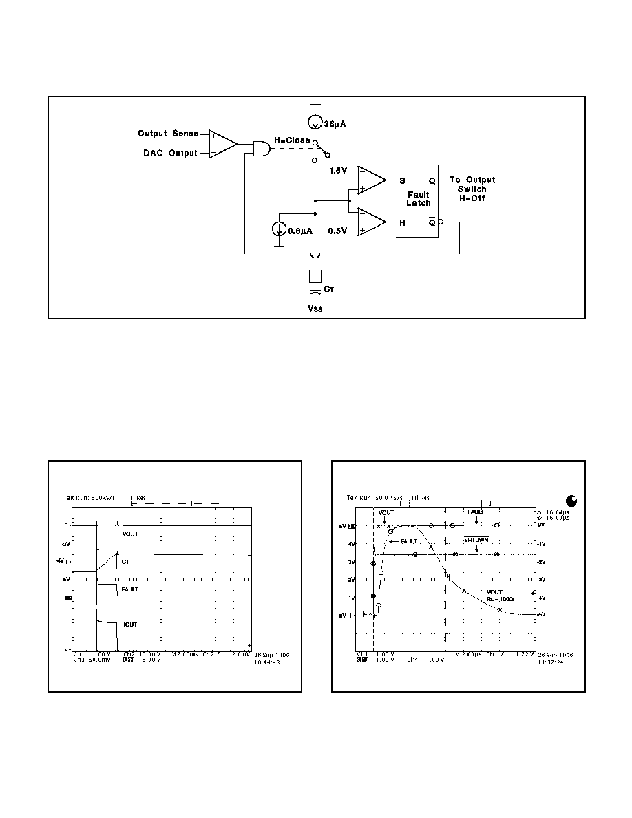
UCC3920 ON TIME CONTROL CIRCUITRY
The overcurrent comparator senses both the DAC out-
put and a representation of the output current. When
the output current exceeds the programmed level the
timing capacitor C
T
charges with 36
µ
A of current. If
the fault occurs for the time it takes for C
T
to charge
up to 1.5V, the fault latch is set and the output switch
is opened. The output remains opened until C
T
dis-
charges to 0.5V with a 0.6
µ
A current source. Once the
0.5V is reached the output is enabled and will either
appear as a switch, if the fault is removed, or a current
source if the fault remains. If the over current condition
is still present then C
T
will begin charging, starting the
cycle over, resulting in approximately a 2% duty cycle.
UDG-96238-1
UCC3920 TYPICAL PERFORMANCE
Shutdown to VOUT Delay (VOUT Turning On)
I
FAULT
Response
5

UCC2920
UCC3920
UNITRODE CORPORATION
7 CONTINENTAL BLVD.
∑
MERRIMACK, NH 03054
TEL. (603) 424-2410
∑
FAX (603) 424-3460
UCC3920 TYPICAL PERFORMANCE (cont.)
Hot Swap of VSS (Input)
Shutdown to Fault and VOUT Delay
(VOUT Turning Off)
Hot Swap of VOUT
Although the UCC3920 is designed to provide system
protection for all fault conditions, all integrated circuits
can ultimately fail short. For this reason, if the
UCC3920 is intended for use in safety critical applica-
tions where UL or some other safety rating is required,
a redundant safety device such as a fuse should be
placed in series with the device. The UCC3920 will pre-
vent the fuse from blowing for virtually all fault condi-
tions, increasing system reliability and reducing main-
tenance cost, in addition to providing the hot swap
benefits of the device.
SAFETY RECOMMENDATION
6

IMPORTANT NOTICE
Texas Instruments and its subsidiaries (TI) reserve the right to make changes to their products or to discontinue
any product or service without notice, and advise customers to obtain the latest version of relevant information
to verify, before placing orders, that information being relied on is current and complete. All products are sold
subject to the terms and conditions of sale supplied at the time of order acknowledgement, including those
pertaining to warranty, patent infringement, and limitation of liability.
TI warrants performance of its semiconductor products to the specifications applicable at the time of sale in
accordance with TI's standard warranty. Testing and other quality control techniques are utilized to the extent
TI deems necessary to support this warranty. Specific testing of all parameters of each device is not necessarily
performed, except those mandated by government requirements.
CERTAIN APPLICATIONS USING SEMICONDUCTOR PRODUCTS MAY INVOLVE POTENTIAL RISKS OF
DEATH, PERSONAL INJURY, OR SEVERE PROPERTY OR ENVIRONMENTAL DAMAGE ("CRITICAL
APPLICATIONS"). TI SEMICONDUCTOR PRODUCTS ARE NOT DESIGNED, AUTHORIZED, OR
WARRANTED TO BE SUITABLE FOR USE IN LIFE-SUPPORT DEVICES OR SYSTEMS OR OTHER
CRITICAL APPLICATIONS. INCLUSION OF TI PRODUCTS IN SUCH APPLICATIONS IS UNDERSTOOD TO
BE FULLY AT THE CUSTOMER'S RISK.
In order to minimize risks associated with the customer's applications, adequate design and operating
safeguards must be provided by the customer to minimize inherent or procedural hazards.
TI assumes no liability for applications assistance or customer product design. TI does not warrant or represent
that any license, either express or implied, is granted under any patent right, copyright, mask work right, or other
intellectual property right of TI covering or relating to any combination, machine, or process in which such
semiconductor products or services might be or are used. TI's publication of information regarding any third
party's products or services does not constitute TI's approval, warranty or endorsement thereof.
Copyright
©
1999, Texas Instruments Incorporated