
UCC29411, UCC29412, UCC29413, UCC39411, UCC39412, UCC39413
LOW POWER SYNCHRONOUS BOOST CONVERTER
SLUS245D ≠ MARCH 2000 ≠ REVISED NOVEMBER 2000
1
POST OFFICE BOX 655303
∑
DALLAS, TEXAS 75265
D
1-V Input Voltage Operation Start-Up
Ensured Under Full Load on Main Output,
and Operation Down to 0.5 V
D
200-mW Output Power at Battery Voltages
as Low as 0.8 V
D
Secondary 7-V Supply from a Single
Inductor
D
Output Fully Disconnected in Shutdown
D
Adaptive Current Mode Control for
Optimum Efficiency
D
High Efficiency Over Wide Operating Range
D
6-
µ
A Shutdown Supply Current
D
Output Reset Function with Programmable
Reset Period
description
The UCCx9411 family of low-input voltage, single-inductor-boost converters is optimized to operate from a
single or dual alkaline cell, and steps up to a 3.3-V, 5-V, or adjustable output at 200 mW. The UCCx9411 family
also provides an auxiliary 7-V output, primarily for the gate-drive supply, which can be used for applications
requiring an auxiliary output, such as 5 V, by linear regulating. The primary output starts up under full load at
input voltages typically as low as 0.8 V with a ensured max of 1 V, and operates down to 0.5 V once the converter
is operating, thereby maximizing battery usage.
simplified block diagram and application circuit
1
4
7
6
VOUT
GND
3.3 V 200 mW
5
RRES
3
100
µ
F
RESET CONTROL CIRCUIT
GLITCH SUPRESSION
PROGRAMMABLE TIMING
MODULATOR CONTROL CIRCUIT
SYNCHRONOUS RECTIFICATION CIRCUITRY
ANTI≠CROSS CONDUCTION
START≠UP
MULTIPLEXING LOGIC
MAX INPUT POWER CONTROL
ADAPTIVE CURRENT CONTROL
START≠UP
CIRCUITRY
1.2
CT
RESB
2
SD/FB
100
µ
F
VIN
SW
8
VGD
0.5
100
µ
F
1 V TO 3.5 V
22
µ
H
+
CT
NOTE A: Pinout shown is for the TSSOP Package. Consult Package Descriptions for the DIP and SOIC configurations.
Copyright
2000, Texas Instruments Incorporated
PRODUCTION DATA information is current as of publication date.
Products conform to specifications per the terms of Texas Instruments
standard warranty. Production processing does not necessarily include
testing of all parameters.
Please be aware that an important notice concerning availability, standard warranty, and use in critical applications of
Texas Instruments semiconductor products and disclaimers thereto appears at the end of this data sheet.
1
2
3
4
8
7
6
5
VIN
SD/FB
RESB
CT
VGD
VOUT
SW
GND
PW PACKAGE
(TOP VIEW)
1
2
3
4
8
7
6
5
VOUT
VGD
VIN
SD/FB
SW
GND
CT
RESB
D OR N PACKAGE
(TOP VIEW)
UCC29411, UCC29412, UCC29413, UCC39411, UCC39412, UCC39413
LOW POWER SYNCHRONOUS BOOST CONVERTER
SLUS245D ≠ MARCH 2000 ≠ REVISED NOVEMBER 2000
2
POST OFFICE BOX 655303
∑
DALLAS, TEXAS 75265
description (continued)
The UCCx9411 family is designed to accommodate demanding applications such as pagers and cell phones
that require high efficiency over a wide operating range of several milli-watts to a couple of hundred milli-watts.
High efficiency at low output current is achieved by optimizing switching and conduction losses with a low total
quiescent current. At higher output current, the 0.5-
switch and 1.2-
synchronous rectifier along with
continuous mode conduction provide high power efficiency. The wide input voltage range of the UCCx9411
family can accommodate other power sources such as NiCd and NimH.
The UCCx9411 family also provides shutdown control. Packages available are the 8-pin SOIC (D), 8-pin
DIP (N), and 8-pin TSSOP (PW) to optimize board space.
absolute maximum ratings over operating free-air temperature (unless otherwise noted)
Input voltage, VIN
≠0.3 V to 10 V
. . . . . . . . . . . . . . . . . . . . . . . . . . . . . . . . . . . . . . . . . . . . . . . . . . . . . . . . . . . . . . . . .
Input voltage, SD
≠0.3 V to V
IN
. . . . . . . . . . . . . . . . . . . . . . . . . . . . . . . . . . . . . . . . . . . . . . . . . . . . . . . . . . . . . . . . . .
Input voltage, VGD
≠0.3 V to 14 V
. . . . . . . . . . . . . . . . . . . . . . . . . . . . . . . . . . . . . . . . . . . . . . . . . . . . . . . . . . . . . . . .
Input voltage, SW
≠0.3 V to 15 V
. . . . . . . . . . . . . . . . . . . . . . . . . . . . . . . . . . . . . . . . . . . . . . . . . . . . . . . . . . . . . . . . .
Output voltage, V
OUT
≠0.3 V to 10 V
. . . . . . . . . . . . . . . . . . . . . . . . . . . . . . . . . . . . . . . . . . . . . . . . . . . . . . . . . . . . .
Stresses beyond those listed under "absolute maximum ratings" may cause permanent damage to the device. These are stress ratings only, and
functional operation of the device at these or any other conditions beyond those indicated under "recommended operating conditions" is not
implied. Exposure to absolute-maximum-rated conditions for extended periods may affect device reliability.
Currents are positive into, negative out of the specific terminal. Consult Packaging Section of the Portable Products Data Book (TI Literature
Number SLUD001) for thermal limitations and considerations of packages.
AVAILABLE OPTIONS
Package PW
Package D or N
TJ
Output Voltage
Output Voltage
TJ
ADJ
3.3 V
5 V
ADJ
3.3 V
5 V
≠40
∞
C to 85
∞
C
29411PW
29412PW
29413PW
29411D
29411N
29412D
29412N
29413D
29413N
0
∞
C to 70
∞
C
39411PW
39412PW
39413PW
39411D
39411N
39412D
39412N
39413D
39413N

UCC29411, UCC29412, UCC29413, UCC39411, UCC39412, UCC39413
LOW POWER SYNCHRONOUS BOOST CONVERTER
SLUS245D ≠ MARCH 2000 ≠ REVISED NOVEMBER 2000
3
POST OFFICE BOX 655303
∑
DALLAS, TEXAS 75265
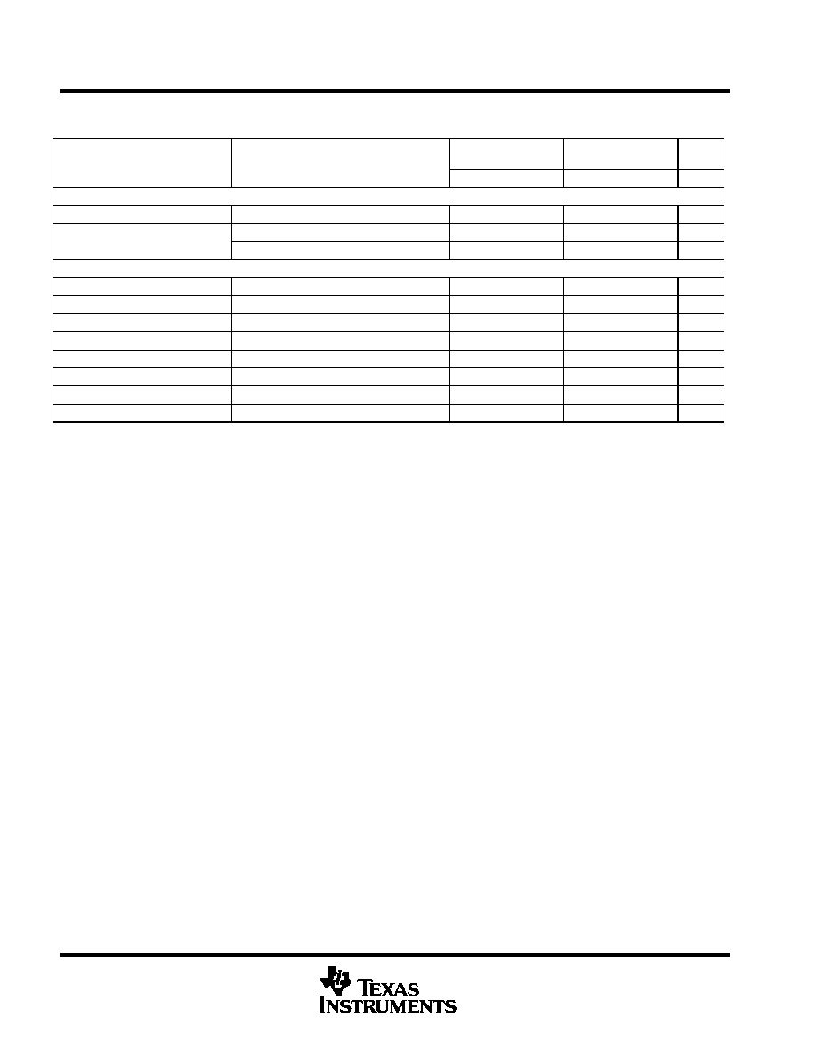
electrical characteristics, T
J
= 0
∞
C to 70
∞
C for the UCC3941x, T
J
= ≠40
∞
C to 85
∞
C for the UCC2941x,
V
IN
= 1.25 V for UCC39411, UCC39412, V
IN
= 2.5 V for the UCC39413, T
A
= T
J
PARAMETER
TEST CONDITIONS
UCC3941x
UCC1941x
UCC2941x
UNITS
PARAMETER
TEST CONDITIONS
MIN
TYP
MAX
MIN
TYP
MAX
UNITS
Input Voltage Section
Minim m start p oltage
No external VGD load,
TJ = 25
∞
C,
IOUT = 60 mA
See Note 1
0.8
1
0.08
1
V
Minimum start-up voltage
No external VGD load,
IOUT = 60 mA
See Note 1
0.9
1.1
1.2
1.4
V
Minimum dropout voltage
No external VGD load, IOUT = 10 mA
See Note 1
0.5
0.7
V
Input voltage range
1.1
3.2
1.3
3.2
V
Quiescent supply current
See Note 2
6
12
8
16
µ
A
Supply current at shutdown
SD = GND
6
12
8
16
µ
A
Output Section
Quiescent supply current
See Note 2
15
28
20
37
µ
A
Supply current at shutdown
SD = GND
3
6
5
10
µ
A
1 V < VIN < 3 V
3.2
3.3
3.39
3.15
3.3
3.45
V
Regulation voltage (UCC39412)
1 V < VIN < 3 V,
0 mA < IOUT < 60 mA
See Note 1
3.17
3.3
3.43
3.11
3.3
3.5
V
1 V < VIN < 5 V
4.85
5
5.15
4.78
5
5.23
V
Regulation voltage (UCC39413)
1 V < VIN < 5 V,
0 mA < IOUT < 60 mA
See Note 1
4.8
5
5.2
4.71
5
5.3
V
ADJ voltage (UCC39411)
1 V < VIN < 3 V
1.212
1.25
1.288
1.194
1.25
1.306
V
Maximum output voltage
(UCCx9411)
5.5
5.5
V
VGD Output Section
Quiescent supply current
See Note 2
20
40
27
55
µ
A
Supply current at shutdown
SD = GND
20
40
27
55
µ
A
1 V < VIN < 3 V
6.3
7
7.7
6.3
7
7.7
V
Regulation voltage (UCC39411/2)
1 V < VIN < 3 V,
0 mA < IOUT < 10 mA
See Note 1
6.3
7
7.7
6.3
7
7.7
V
1 V < VIN < 5 V
7.7
8.5
9.3
7.7
8.5
9.3
V
Regulation voltage (UCC39413)
1 V < VIN < 5 V,
0 mA < IOUT < 10 mA
See Note 1
7.7
8.5
9.3
7.7
8.5
9.3
V
Inductor Charging Section (L = 22
µ
H)
Peak discontinuous current
Operating range,
L = 22.1
µ
H
180
250
300
180
250
300
mA
Peak continuous current
385
550
715
385
550
715
mA
Charge switch RDS(on)
D package
0.5
0.75
0.6
0.85
Current limit delay
See Note 1
50
50
ns
Synchronous Rectifier Section
Rectifier RDS(on)
D package
1.2
1.8
1.4
2.16
NOTES:
1. Ensured by design. Not production tested.
2. For the UCC39411 FB = 1.306 V, VGD = 7.7 V, For the UCC39412 VOUT = 3.5 V and VGD = 7.7 V, For the UCC39413 VOUT = 5.3 V,
VGD=9.3 V
.
UCC29411, UCC29412, UCC29413, UCC39411, UCC39412, UCC39413
LOW POWER SYNCHRONOUS BOOST CONVERTER
SLUS245D ≠ MARCH 2000 ≠ REVISED NOVEMBER 2000
4
POST OFFICE BOX 655303
∑
DALLAS, TEXAS 75265
electrical characteristics, T
J
= 0
∞
C to 70
∞
C for the UCC3941x, T
J
= ≠40
∞
C to 85
∞
C for the UCC2941x,
V
IN
= 1.25 V for UCC39411, UCC39412, V
IN
= 2.5 V for the UCC39413, T
A
= T
J
(continued)
PARAMETER
TEST CONDITIONS
UCC3941x
UCC1941x
UCC2941x
UNITS
PARAMETER
TEST CONDITIONS
MIN
TYP
MAX
MIN
TYP
MAX
UNITS
Shutdown Section
Threshold
0.4
0.6
0.8
0.2
0.6
0.9
V
Inp t bias c rrent
SD = GND
2
5
15
2
5
15
µ
A
Input bias current
SD = 1.25 V
5
20
20
100
nA
Reset Section
Threshold (UCC39411)
1.08
1.125
1.17
1.07
1.125
1.18
V
Threshold (UCC39412)
2.85
2.97
3.09
2.83
2.97
3.11
V
Threshold (UCC39413)
4.32
4.5
4.68
4.3
4.5
4.7
V
Reset period
CT = 0.15
µ
F
113
188
300
94
188
300
ms
VOUT to reset delay
VOUT falling at ≠1 mV/
µ
s,
See Note 1
60
60
µ
s
Sink current
1
20
1
20
mA
Output low voltage
IOUT = 500
µ
A
0.1
0.1
V
Output leakage
0.5
0.5
µ
A
NOTES:
1. Ensured by design. Not production tested.
2. For the UCC39411 FB = 1.306 V, VGD = 7.7 V, For the UCC39412 VOUT = 3.5 V and VGD = 7.7 V, For the UCC39413 VOUT = 5.3 V,
VGD=9.3 V
.
pin assignments
VIN: Input voltage to supply the IC during start-up. After the output is running the IC draws power from VOUT
or VGD.
SW: An inductor is connected between this pin and VIN. The VGD (gate drive supply) flyback diode is also
connected to this pin. When servicing the main output supply this pin pulls low, charging the inductor, then shuts
off dumping the energy through the synchronous rectifier to the output. When servicing the VGD supply, the
internal synchronous rectifier stays off and the energy is diverted to VGD through the flyback diode. During
discontinuous portions of the inductor current, a MOSFET resistively connects VIN to SW damping excess
circulating energy to eliminate undesired high-frequency ringing.
VGD: The VGD pin, which is coarsely regulated around 7 V (8.5 V for the UCC39413), is primarily used for the
gate drive supply for the power switches in the IC. This pin can be loaded with up to 10 mA as long as it does
not present a load at voltages below 2 V (this ensures proper start-up of the IC). The VGD supply can go as
low as 6.3 V without interfering with the servicing of the main output. When below 6.3 V, VGD has the highest
priority.
VOUT: Main output voltage (3.3 V, 5 V, or adjustable), has highest priority in the multiplexing scheme, as long
as VGD is above the critical level of 6.3 V. Startup at full load is achievable at input voltages down to 1 V.
CT: This pin provides the timer for determining the reset period. The period is controlled by placing a capacitor
to ground of value C = (0.81e
≠6
)
◊
t where t is the desired reset period.
RESB: This pin provides an active low signal to alert the user when the main output voltage falls below 10%
of its targeted value. The open-drain output can be used to reset a microcontroller that may be powered off of
the main output voltage.
SD/FB: For the UCC39411, this pin is used to adjust the output voltage via a resistive divider from VOUT. It also
serves as the shutdown pin for all three versions. Pulling this pin low provides a shutdown signal to the IC.
GND: Ground of the IC.
UCC29411, UCC29412, UCC29413, UCC39411, UCC39412, UCC39413
LOW POWER SYNCHRONOUS BOOST CONVERTER
SLUS245D ≠ MARCH 2000 ≠ REVISED NOVEMBER 2000
5
POST OFFICE BOX 655303
∑
DALLAS, TEXAS 75265
APPLICATION INFORMATION
operation
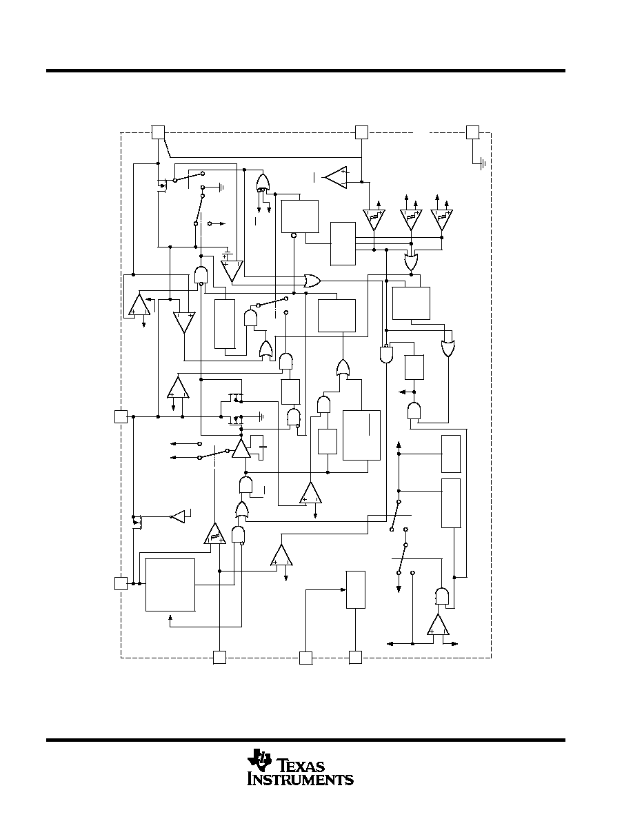
A detailed block diagram of the UCC39411 is shown in Figure 1. Unique control circuitry provides high-efficiency
power conversion for both light and heavy loads by transitioning between discontinuous and continuous
conduction based on load conditions. Figure 2 depicts converter waveforms for the application circuit shown
in Figure 3. A single 22-
µ
H inductor provides the energy pulses required for a highly efficient 3.3-V converter
at up to 200-mW output power.
At time t1, the 3.3-V output voltage has dropped below its lower threshold, and the inductor is charged with an
on time determined by: t
ON
= 5.5
µ
s/VIN. For a 1.25-V input and a 22-
µ
H inductor, the resulting peak current
is approximately 250 mA. At time t2, the inductor begins to discharge with a minimum off time of approximately
1 ms. Under lightly loaded conditions, the amount of energy delivered in this single pulse satisfies the
voltage-control loop, and the converter does not command any more energy pulses until the output again drops
below the lower-voltage threshold.
At time t3, the VGD supply drops below its lower threshold, but the output voltage is still above its threshold point.
This results in an energy pulse to the gate-drive supply at t4. In some cases, a single pulse supplied to VGD
is insufficient to raise the VGD voltage level enough to satisfy the voltage loop. Under this condition, multiple
pulses are supplied to VGD. Note that when the UCC3941x is servicing VGD only, the IC maintains a
discontinuous mode of operation. After time t4, the 3.3-V output drops below its threshold and requests to be
serviced once the VGD cycle has completed, which occurs at time t5.
Time t6 represents a transition between light load and heavy load. A single energy pulse is not sufficient to force
the output voltage above its upper threshold before the minimum off time has expired and a second charge cycle
is commanded. Since the inductor current does not reach zero in this case, the peak current is greater than
250 mA at the end of the next charge on time. The result is a ratcheting of inductor current until either the output
voltage is satisfied, or the converter reaches its set current limit. At time t7, the gate drive voltage has dropped
below its 7-V threshold but the converter continues to service the output because it has higher priority unless
VGD drops below
6.3 V.
Between time t7 and t8, the converter reaches its peak current limit.
Once the peak current is reached, the converter operates in continuous mode with approximately 60-mA of
inductor current ripple. At time t8, the 3.3-V output is satisfied and the converter can service the gate drive
voltage, VGD, which occurs at time t9.
UCC2941
1,
UCC29412,
UCC29413,
UCC3941
1,
UCC39412,
UCC39413
LOW
POWER
SYNCHRONOUS
BOOST
CONVERTER
SLUS245D
≠
MARCH 2000
≠
REVISED NOVEMBER 2000
6
POST
OFFICE BOX 655303
∑
DALLAS, TEXAS 75265
APPLICA
TION INFORMA
TION
1
3
VGD
SD/FB
VOUT
0.5V
VGD
8
RESET
4
5
2
200 kHZ
START≠UP
OSCILLATOR
AND
CONTROL
VLOW
SW
1.25 V (UCC39411)
3.3 V (UCC39412)
5.0 V (UCC39413)
PRIORITY
ENCODER
VGD
7.5 V (UCC39411/2)
8.5 V (UCC39413)
VGD
6 V (UCC39411/2)
7.5 V (UCC39413)
SD
CLK
D
Q
FROM SD
VREF GOOD
1-
µ
s RISING
EDGE DELAY
R
S
D
Q
R
SD
Q
1
µ
s
R.E.D.
VON
INTERNAL
BIAS
1.25 V
REFERENCE
2.5 V
VGD
VDD
RESET
TIMER
CT
6
CT
5 V GS
VREF
GOOD
FROM SD
RISING EDGE
DELAY
TON= 5.5 E
≠6
VBAT
50 ns
R.E.D.
0.66 A
MAX
CPUMP
VBAT
t OFF TIMER
50 ns
R.E.D.
VON
VIN
VBAT
VGD
VGD
1.2
VOUT
7
Figure 1. Low Power Synchronous Boost
NOTE A:
Switches are shown in the low state. Pinouts as shown is for the 8-pin D, J, or N. See package descriptions for 8-pin SO
IC.

UCC29411, UCC29412, UCC29413, UCC39411, UCC39412, UCC39413
LOW POWER SYNCHRONOUS BOOST CONVERTER
SLUS245D ≠ MARCH 2000 ≠ REVISED NOVEMBER 2000
7
POST OFFICE BOX 655303
∑
DALLAS, TEXAS 75265
APPLICATION INFORMATION
VGD
RIPPLE
50 mV/DIV
7 V
t1
t2
t3
t4
t5
t6
t7
t8
t9
INDUCTOR
CURRENT
CURRENT
LIMIT
OUTPUT
RIPPLE
20 mV/DIV
3.3 V
HIGH LOAD CURRENT
LIGHT LOAD CURRENT
200 mVP≠P
TYPICAL
20 mV
TYPICAL
P≠P
Figure 2. Inductor Current and Output Ripple Waveforms
UDG≠98069
1
2
7
6
GND
L = 10
µ
H TO 100
µ
H
5
R1
100
µ
F
4
SD/FB
10
µ
F
VIN
SW
8
VGD
10
µ
F
1≠2 CELL ALKALINE
1.0 V TO 3.2 V
3
80 nF
100 k
VOUT
CT
RESB
R2
VOUT
Figure 3. Low Power Synchronous Boost Converter ADJ Version ≠200 mW
NOTE A: Pinout shown is for the TSSOP Package. Consult Package Descriptions for the DIP and SOIC configurations.
UCC29411, UCC29412, UCC29413, UCC39411, UCC39412, UCC39413
LOW POWER SYNCHRONOUS BOOST CONVERTER
SLUS245D ≠ MARCH 2000 ≠ REVISED NOVEMBER 2000
8
POST OFFICE BOX 655303
∑
DALLAS, TEXAS 75265
APPLICATION INFORMATION
shutdown control
Shutdown of the UCC3941x is controlled via the interface with the SD/FB pin. Pulling the SD/FB pin low, for all
versions, causes the IC to go into shutdown. In the UCC39412 and UCC39413, the SD/FB pin is used solely
as a shutdown function. Therefore, the SD/FB pin for the UCC39412 and UCC39413 can be directly controlled
using conventional CMOS or transistor to transistor logic (TTL) technology. For the UCC39411, interface into
the SD/FB is slightly more complicated due to the added feedback function. When feeding back the output
voltage to the SD/FB pin on the UCC39411, the IC requires a Thevenin impedance of at least 200-k
(500-k
for industrial/military applications) to ground. Then, to accomplish shutdown of the IC, an open-drain device may
be used.
component selection inductor selection
An inductor value of 22
µ
H works well in most applications, but values between 10
µ
H to 100
µ
H are also
acceptable. Lower value inductors typically offer lower ESR and smaller physical size. Due to the nature of the
"bang-bang" controllers, larger inductor values typically result in larger overall voltage ripple, because once the
output voltage level is satisfied the converter goes discontinuous, resulting in the residual energy of the inductor
causing overshoot.
It is recommended to keep the ESR of the inductor below 0.15
for 200-mW applications. A Coilcraft
DT3316P-223 surface-mount inductor is acceptable because it has a current rating of 1.5 A and an ESR of 84
m
.
Other choices for surface-mount inductors are shown in Table 1.
Table 1. Inductor Suppliers
MANUFACTURER
PART NUMBERS
Coilcraft
DT Series
Cary, Illinois
Tel: 708≠639≠2361
Fax: 708≠639≠1469
Coiltronics
CTX Series
Boca Raton, Florida
Tel: 407≠241≠7876
output capacitor selection
Once the inductor value is selected, the capacitor value determines the ripple of the converter. The worst case
peak-to-peak ripple of a cycle is determined by two components, one is due to the charge storage characteristic,
and the other is the ESR of the capacitor. The worst case ripple occurs when the inductor is operating at max
current and is expressed as follows:
D
V
+
I
CL
2
L
2C V
O
*
V
I
)
I
CL
C
ESR

UCC29411, UCC29412, UCC29413, UCC39411, UCC39412, UCC39413
LOW POWER SYNCHRONOUS BOOST CONVERTER
SLUS245D ≠ MARCH 2000 ≠ REVISED NOVEMBER 2000
9
POST OFFICE BOX 655303
∑
DALLAS, TEXAS 75265
APPLICATION INFORMATION
output capacitor selection (continued)
∑
I
CL
= the peak inductor current = 550 mA
∑
V = Output ripple
∑
V
O
= Output voltage
∑
V
I
= Input voltage
∑
C
ESR
= ESR of the output capacitor
A Sanyo OS-CON series surface-mount capacitor (10SN100M) is acceptable. It has an ESR rating of 90 m
at 100
µ
F.
Other potential capacitor sources are shown in Table 2.
Table 2. Capacitor Supplies
MANUFACTURER
PART NUMBER
Sanyo Video Components
OS≠CON Series
San Diego, California
Tel: 619≠661≠6322
Fax: 619≠661≠1055
AVX
TPS Series
Sanford, Maine
Tel: 207≠282≠5111
Fax: 207≠283≠1941
Sprague
695D Series
Concord, New Hampshire
Tel: 603≠224≠1961
input capacitor selection
Since the UCCx9411 family does not require a large decoupling capacitor on the input voltage to operate
properly, a 10-
µ
F cap is sufficient for most applications. Optimum efficiency occurs when the capacitor value
is large enough to decouple the source impedance, this usually occurs for capacitor values in excess of 100
µ
F.
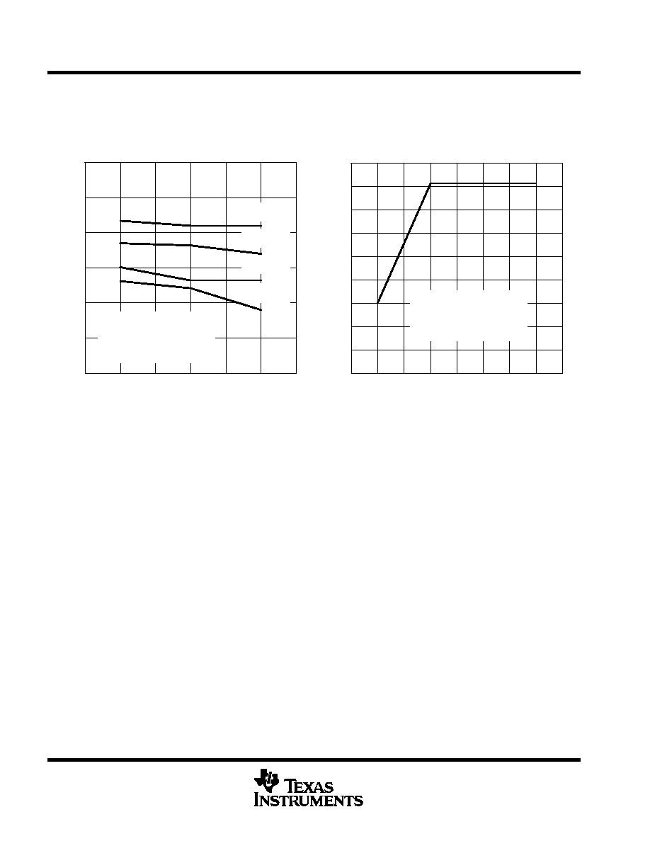
RESET operation
A reset function is provided to prevent the microprocessor from executing code during undervoltage conditions,
typically during power up or power down. The reset voltage threshold is fixed at 90% of the output voltage for
all versions of the UCCx941x. To prevent erratic operation in noisy environments, a glitch filter is provided.
To allow sufficient time for the microprocessor clock to stabilize, a user-programmable reset period is provided.
The reset period, the time from the output voltage rising above 90% of nominal to RESB going high, is
programmed via an external capacitor connected to the CT pin.
The reset period is defined as:
t
RP
+
C
1.25
where C is in
µ
F, and t
RP
is in seconds.
A typical reset profile during power up is shown in Figure 4 and power down in Figure 5.

UCC29411, UCC29412, UCC29413, UCC39411, UCC39412, UCC39413
LOW POWER SYNCHRONOUS BOOST CONVERTER
SLUS245D ≠ MARCH 2000 ≠ REVISED NOVEMBER 2000
10
POST OFFICE BOX 655303
∑
DALLAS, TEXAS 75265
APPLICATION INFORMATION
Figure 4
POWER-UP SEQUENCE
VOUT
RESB
CT
Figure 5
POWER-DOWN SEQUENCE
VOUT
RESB
Figure 6
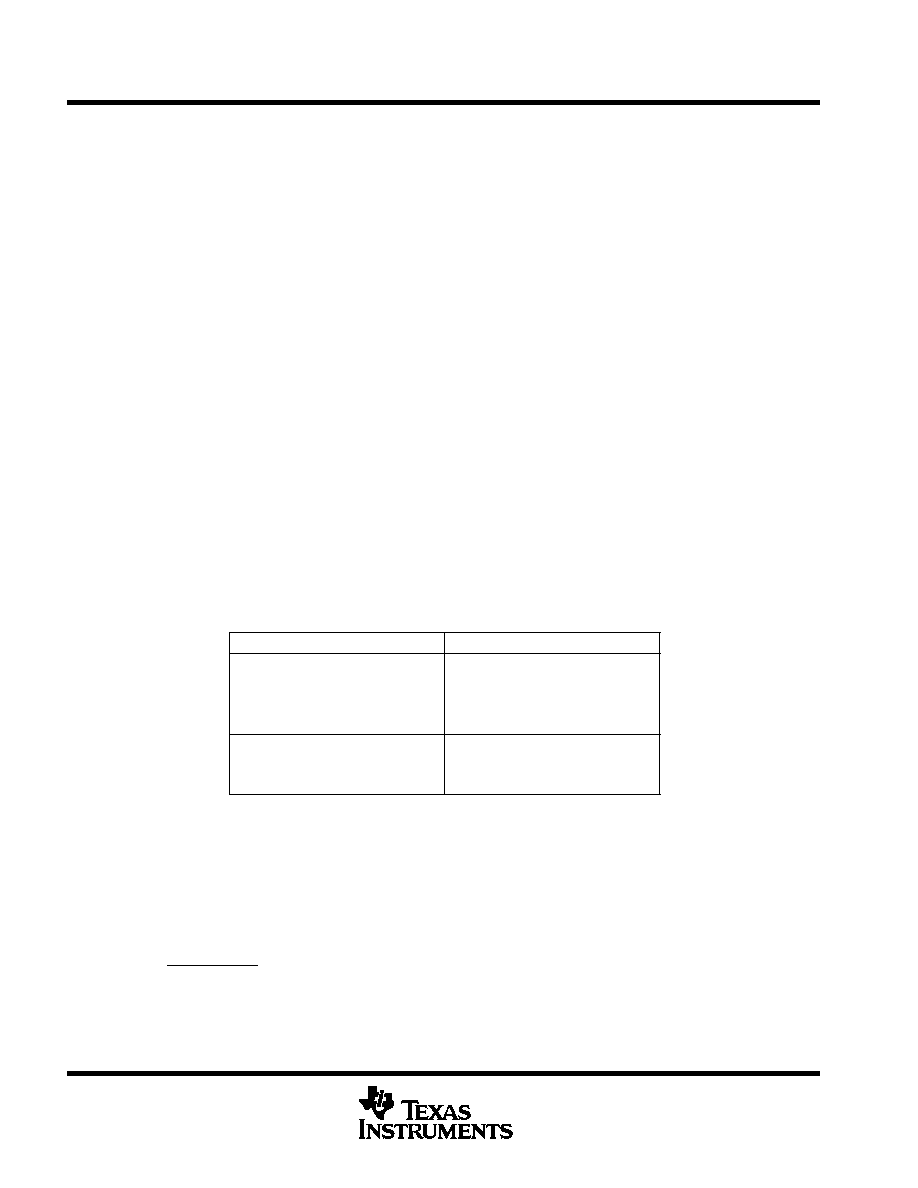
0.04
0.025
0.01
0.001
0.0001
10
20
30
40
50
60
70
80
90
100
0
Load Current ≠ A
0.06
V
IN
= 3.0 V
V
IN
= 2.4 V
V
IN
= 1.2 V
Efficiency
- %
TYPICAL EFFICIENCY
vs
LOAD CURRENT
UCC39411 @ 3.3 VOUT
L = 22
µ
H, DO3316-223
Figure 7
0.04
0.025
0.01
0.001
0.0001
10
20
30
40
50
60
70
80
90
100
0
Load Current ≠ A
0.06
V
IN
= 3.0 V
V
IN
= 2.4 V
V
IN
= 1.2 V
Efficiency - %
UCC39411 @ 3.3 VOUT
L = 22
µ
H, DO1608-223
TYPICAL EFFICIENCY
vs
LOAD CURRENT

UCC29411, UCC29412, UCC29413, UCC39411, UCC39412, UCC39413
LOW POWER SYNCHRONOUS BOOST CONVERTER
SLUS245D ≠ MARCH 2000 ≠ REVISED NOVEMBER 2000
11
POST OFFICE BOX 655303
∑
DALLAS, TEXAS 75265
APPLICATION INFORMATION
Figure 8
0.04
0.03
0.02
0.01
0.001
0.0001
10
20
30
40
50
60
70
80
90
100
0
Load Current ≠ A
V
IN
= 3.0 V
V
IN
= 2.4 V
V
IN
= 1.2 V
0.06
Efficiency
- %
UCC39412 L = 22
µ
H,
DO3316-223
TYPICAL EFFICIENCY
vs
LOAD CURRENT
Figure 9
0.04
0.03
0.02
0.01
0.001
0.0001
10
20
30
40
50
60
70
80
90
100
0
Load Current ≠ A
V
IN
= 3.0 V
V
IN
= 2.4 V
V
IN
= 1.2 V
Efficiency
- %
UCC39413 L = 15
µ
H,
DO3316-153
TYPICAL EFFICIENCY
vs
LOAD CURRENT
Figure 10
0.04
0.03
0.02
0.01
0.001
0.0001
10
20
30
40
50
60
70
80
90
100
0
Load Current ≠ A
V
IN
= 3.0 V
V
IN
= 2.4 V
V
IN
= 1.2 V
0.06
Efficiency
- %
UCC39412 L = 22
µ
H,
DO1608-223
TYPICAL EFFICIENCY
vs
LOAD CURRENT
Figure 11
0.04
0.03
0.02
0.01
0.001
0.0001
10
20
30
40
50
60
70
80
90
100
V
IN
= 3.0 V
V
IN
= 1.2 V
V
IN
= 2.4 V
0
Efficiency
- %
Load Current ≠ mA
UCC39413 L = 15
µ
H,
DO1608-153
TYPICAL EFFICIENCY
vs
LOAD CURRENT
UCC29411, UCC29412, UCC29413, UCC39411, UCC39412, UCC39413
LOW POWER SYNCHRONOUS BOOST CONVERTER
SLUS245D ≠ MARCH 2000 ≠ REVISED NOVEMBER 2000
12
POST OFFICE BOX 655303
∑
DALLAS, TEXAS 75265
APPLICATION INFORMATION
Figure 12
150
100
75
75
80
85
90
95
100
70
Load Current ≠ mA
V
IN
= 3.0 V
V
IN
= 2.0 V
V
IN
= 1.8 V
V
IN
= 2.5 V
Efficiency
- %
UCC39411 @ 3.3 VOUT
L = DO1608-223
TYPICAL EFFICIENCY
vs
LOAD CURRENT (TWO CELL
APPLICATION)
Figure 13
2.5
2.0
1.8
115
120
125
130
135
140
145
150
155
110
Input Voltage ≠ V
3.0
Load
Current - mA
MAXIMUM LOAD CURRENT,
2 CELL APPLICATION
vs
INPUT CURRENT
UCC39411 @ 3.3 VOUT
L = DO1608-223

IMPORTANT NOTICE
Texas Instruments and its subsidiaries (TI) reserve the right to make changes to their products or to discontinue
any product or service without notice, and advise customers to obtain the latest version of relevant information
to verify, before placing orders, that information being relied on is current and complete. All products are sold
subject to the terms and conditions of sale supplied at the time of order acknowledgment, including those
pertaining to warranty, patent infringement, and limitation of liability.
TI warrants performance of its products to the specifications applicable at the time of sale in accordance with
TI's standard warranty. Testing and other quality control techniques are utilized to the extent TI deems necessary
to support this warranty. Specific testing of all parameters of each device is not necessarily performed, except
those mandated by government requirements.
Customers are responsible for their applications using TI components.
In order to minimize risks associated with the customer's applications, adequate design and operating
safeguards must be provided by the customer to minimize inherent or procedural hazards.
TI assumes no liability for applications assistance or customer product design. TI does not warrant or represent
that any license, either express or implied, is granted under any patent right, copyright, mask work right, or other
intellectual property right of TI covering or relating to any combination, machine, or process in which such
products or services might be or are used. TI's publication of information regarding any third party's products
or services does not constitute TI's approval, license, warranty or endorsement thereof.
Reproduction of information in TI data books or data sheets is permissible only if reproduction is without
alteration and is accompanied by all associated warranties, conditions, limitations and notices. Representation
or reproduction of this information with alteration voids all warranties provided for an associated TI product or
service, is an unfair and deceptive business practice, and TI is not responsible nor liable for any such use.
Resale of TI's products or services with
statements different from or beyond the parameters stated by TI for
that product or service voids all express and any implied warranties for the associated TI product or service,
is an unfair and deceptive business practice, and TI is not responsible nor liable for any such use.
Also see: Standard Terms and Conditions of Sale for Semiconductor Products. www.ti.com/sc/docs/stdterms.htm
Mailing Address:
Texas Instruments
Post Office Box 655303
Dallas, Texas 75265
Copyright
2001, Texas Instruments Incorporated