UCC29421, UCC29422, UCC39421, UCC39422
MULTIMODE HIGH FREQUENCY PWM CONTROLLER
SLUS246C - OCTOBER 1999 - REVISED FEBRUARY 2005
1
POST OFFICE BOX 655303
∑
DALLAS, TEXAS 75265
D
Operation Down to an Input
Voltage of 1.8 V
D
High Efficiency Boost, SEPIC or
Flyback (Buck-Boost) Topologies
D
Drives External FETs for
High-Current Applications
D
Up to 2-MHz Oscillator
D
Synchronizable Fixed Frequency
Operation
D
High-Efficiency Low-Power Mode
D
High-Efficiency at Very Low-Power
with Programmable Variable
Frequency Mode
D
Pulse-by-Pulse Current Limit
D
5-
µ
A Supply Current in Shutdown
D
150-
µ
A Supply Current in Sleep
Mode
D
Selectable NMOS or PMOS
Rectification
D
Built-In Power-On Reset
(UCC39422 Only)
D
Built-In Low-Voltage Detect
(UCC39422 Only)
description
The UCC39421 family of synchronous
PWM controllers is optimized to operate
from dual alkaline/NiCd cells or a single
Lithium-Ion (Li-Ion) cell, and convert to
adjustable output voltages from 2.5 V to
8 V. For applications where the input
voltage does not exceed the output, a
standard boost configuration is used.
For other applications where the input voltage can swing above and below the output, a 1:1 coupled inductor
(Flyback or SEPIC) is used in place of the single inductor. Fixed frequency operation can be programmed, or
synchronized to an external clock source. In applications where (at light loads) variable frequency mode is
acceptable, the IC can be programmed to automatically enter PFM (pulse frequency modulation) mode for an
additional efficiency benefit.
Synchronous rectification provides excellent efficiency at high power levels, where N- or P- type MOSFETs can
be used. At lower power levels (between 10% and 20% of full load) where fixed frequency operation is required,
low power mode is entered. This mode optimizes efficiency by cutting back on the gate drive of the charging
FET. At very low power levels, the IC enters a variable frequency mode (PFM). PFM can be disabled by the user.
Copyright
2000, Texas Instruments Incorporated
PRODUCTION DATA information is current as of publication date.
Products conform to specifications per the terms of Texas Instruments
standard warranty. Production processing does not necessarily include
testing of all parameters.
Please be aware that an important notice concerning availability, standard warranty, and use in critical applications of
Texas Instruments semiconductor products and disclaimers thereto appears at the end of this data sheet.
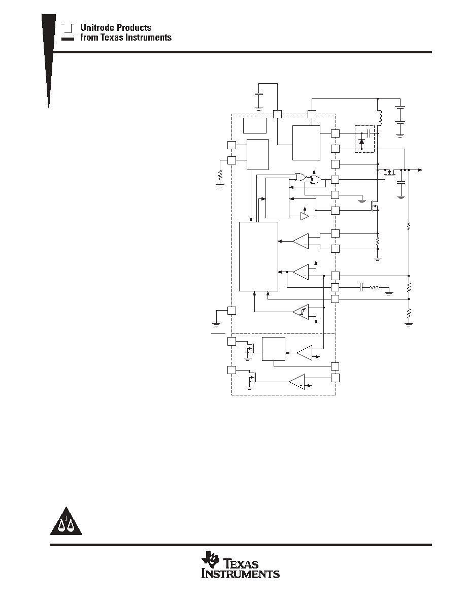
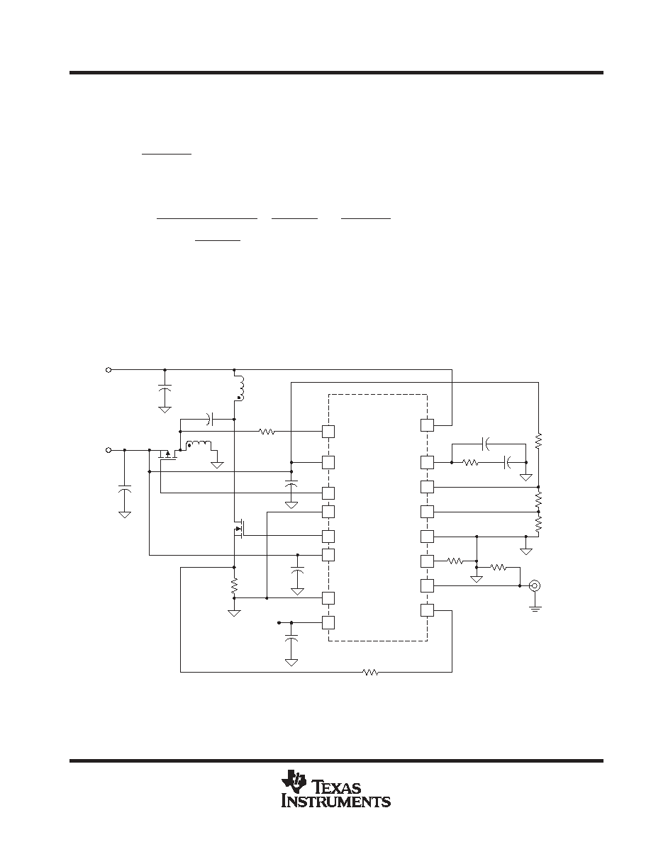
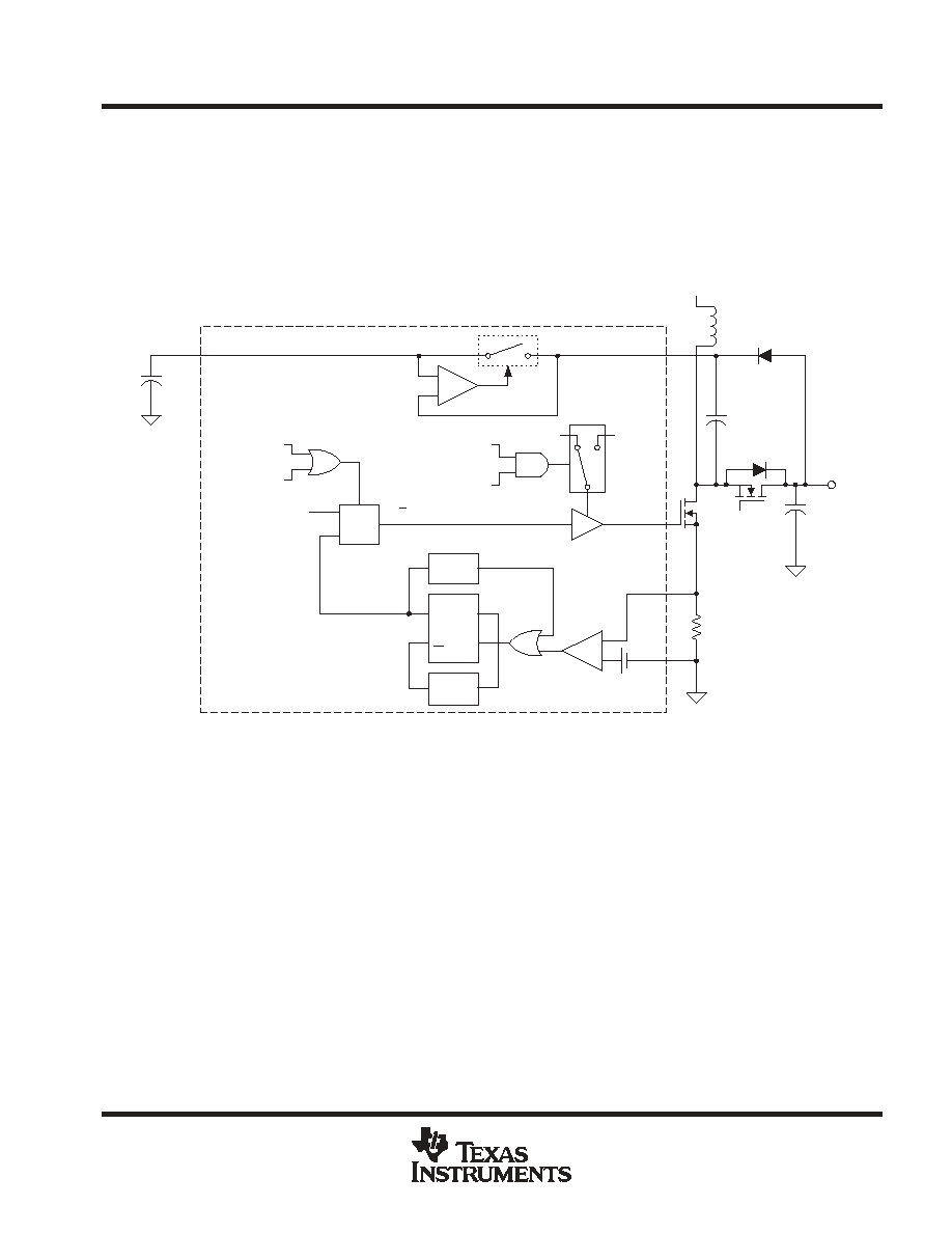
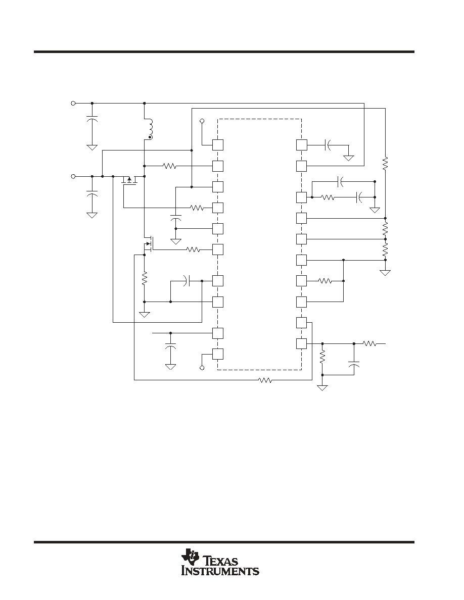
simplified schematic block diagram and
application circuit
UDG-98122
20
4
2
16
18
1
17
5
15
11
19
6
8
9
7
13
14
10
12
+
1.24 V
LOWBAT
+
200 mS
RESET/
POR
1.18 V
VDET
RSADJ
GND
UCC39422
ONLY
RESET
+
1.22V
PWM CIRCUITRY
CURRENT LIMIT
LOW POWER
MODE
SLOPE
COMPENSATION
PFM MODE
CONTROL
+
PFM
COMP
FB
ERROR
AMP
PGND
ISENSE
50 mV TYP
+
X10
ANTI-
CROSS
COND.
CHRG
VPUMP
RSEL
RECT
CHARGE
PUMP
3
CP
VOUT
RSEN
VIN
VPUMP
+
+
2 CELL
ALKALINE/
NiCd OR
1 LI-ION
VOUT
RT
SYNC/SD
PWM
OSC
1.24 V
VREF
VGD
1.24 V
1.8 V(MIN)
UCC29421, UCC29422, UCC39421, UCC39422
MULTIMODE HIGH FREQUENCY PWM CONTROLLER
SLUS246C - OCTOBER 1999 - REVISED FEBRUARY 2005
2
POST OFFICE BOX 655303
∑
DALLAS, TEXAS 75265
description (continued)
Other features include pulse-by-pulse current limiting, and a low 5-
µ
A quiescent current during shutdown. The
UCC39422 incorporates programmable power-on reset circuitry and an uncommitted comparator for low
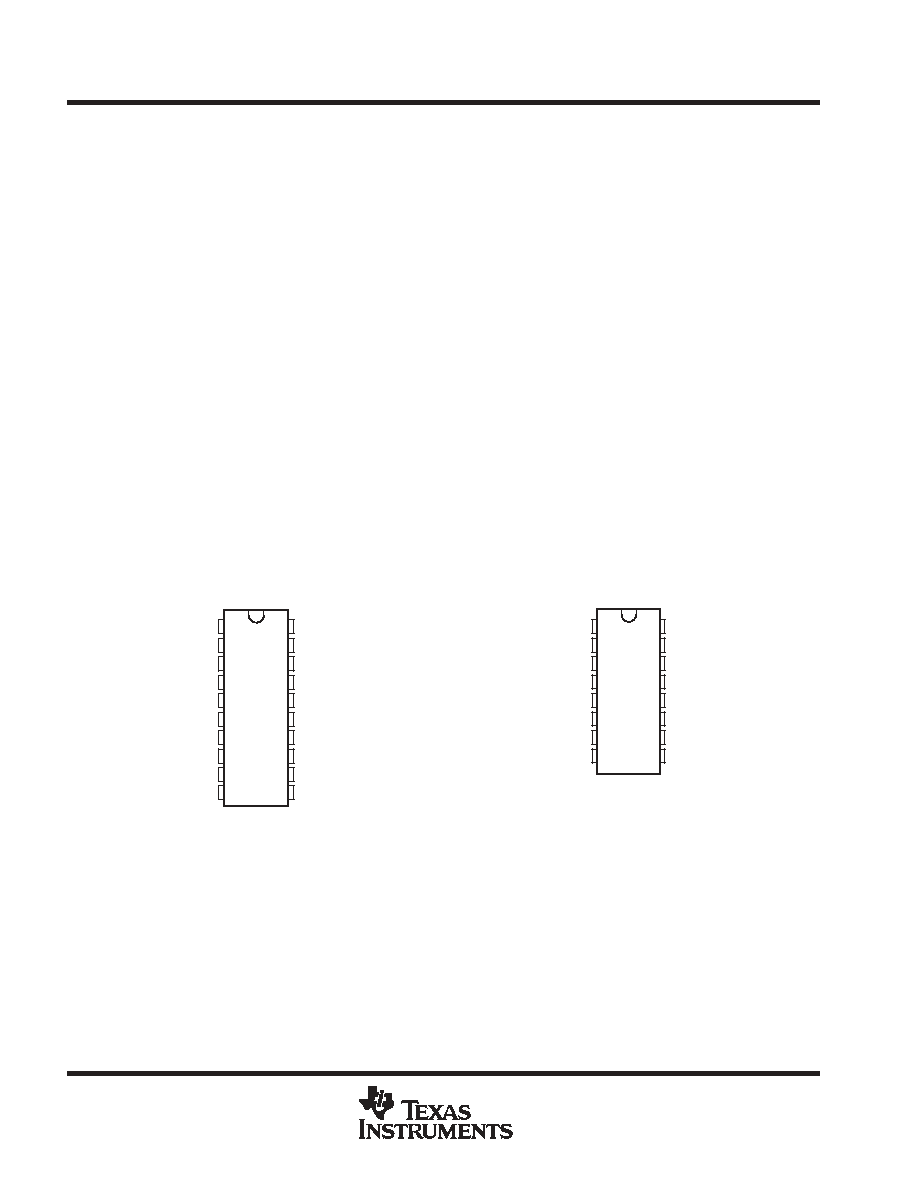
voltage detection. The available packages are 20-pin TSSOP or 20-pin N for the UCC39422, and 16-pin TSSOP
or 16-pin N for the UCC39421.
absolute maximum ratings over operating free-air temperature range (unless otherwise noted)
}
Supply Voltage (VIN, VOUT,VPUMP)
8 V
. . . . . . . . . . . . . . . . . . . . . . . . . . . . . . . . . . . . . . . . . . . . . . . . . . . . . . . . . .
CP
8 V
. . . . . . . . . . . . . . . . . . . . . . . . . . . . . . . . . . . . . . . . . . . . . . . . . . . . . . . . . . . . . . . . . . . . . . . . . . . . . . . . . . . . . . . .
RSEN
≠0.3 V to 12 V
. . . . . . . . . . . . . . . . . . . . . . . . . . . . . . . . . . . . . . . . . . . . . . . . . . . . . . . . . . . . . . . . . . . . . . . . . . .
SYNC/SD
≠0.3 V to 5 V
. . . . . . . . . . . . . . . . . . . . . . . . . . . . . . . . . . . . . . . . . . . . . . . . . . . . . . . . . . . . . . . . . . . . . . . . .
ISENSE
≠0.3 V to 1 V
. . . . . . . . . . . . . . . . . . . . . . . . . . . . . . . . . . . . . . . . . . . . . . . . . . . . . . . . . . . . . . . . . . . . . . . . . .
Storage Temperature, T
stg
≠65
∞
C to 150
∞
C
. . . . . . . . . . . . . . . . . . . . . . . . . . . . . . . . . . . . . . . . . . . . . . . . . . . . . . . .
Junction Temperature, T
J
≠55
∞
C to 150
∞
C
. . . . . . . . . . . . . . . . . . . . . . . . . . . . . . . . . . . . . . . . . . . . . . . . . . . . . . . . .
Lead Temperature (Soldering, 10 seconds)
300
∞
C
. . . . . . . . . . . . . . . . . . . . . . . . . . . . . . . . . . . . . . . . . . . . . . . . . .
Stresses beyond those listed under "absolute maximum ratings" may cause permanent damage to the device. These are stress ratings only, and
functional operation of the device at these or any other conditions beyond those indicated under "recommended operating conditions" is not
implied. Exposure to absolute-maximum-rated conditions for extended periods may affect device reliability.
All voltages are with respect to ground. Currents are positive into and negative out of the specified terminals. Consult the Packaging Section of
the Databook for thermal limitations and considerations of the package.
1
2
3
4
5
6
7
8
9
10
20
19
18
17
16
15
14
13
12
11
RESETB
RSEN
VOUT
RECT
PGND
CHRG
VPUMP
CP
VIN
LOWBAT
RSADJ
RSEL
COMP
FB
PFM
GND
RT
SYNC/SD
ISENSE
VDET
TSSOP-20, DIL-20
N, PW PACKAGES
(TOP VIEW)
1
2
3
4
5
6
7
8
16
15
14
13
12
11
10
9
RSEN
VOUT
RECT
PGND
CHRG
VPUMP
CP
VIN
RSEL
COMP
FB
PFM
GND
RT
SYNC/SD
ISENSE
TSSOP-16, DIL-16
N, PW PACKAGE
(TOP VIEW)
UCC29421, UCC29422, UCC39421, UCC39422
MULTIMODE HIGH FREQUENCY PWM CONTROLLER
SLUS246C - OCTOBER 1999 - REVISED FEBRUARY 2005
3
POST OFFICE BOX 655303
∑
DALLAS, TEXAS 75265
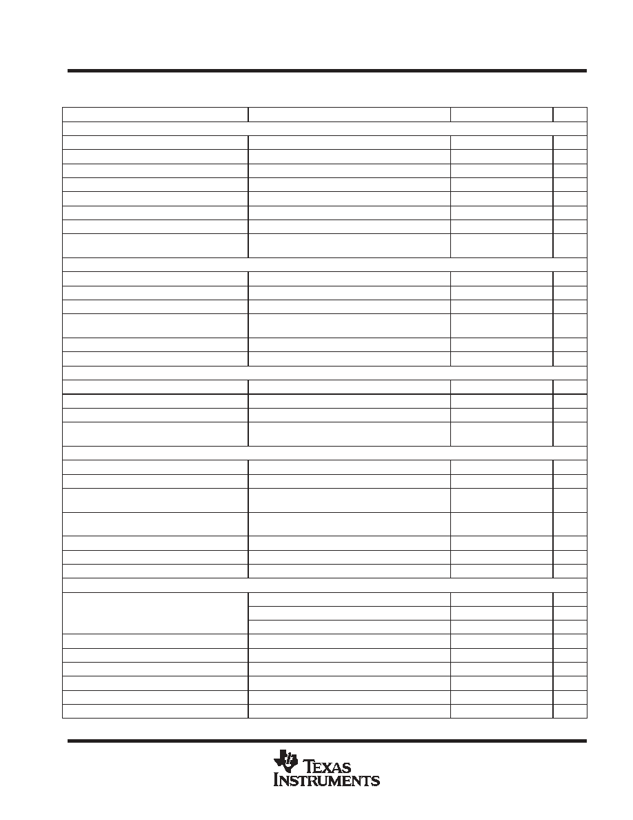
electrical characteristics over recommended operating free-air temperature range, T
A
= -40
∞
C to
85
∞
C for the UCC2942x, 0
∞
C to 70
∞
C for the UCC3942x, R
T
= 100 k
, V
VPUMP
= 6 V, V
VIN
= 3 V.
PARAMETER
TEST CONDITIONS
MIN
TYP
MAX
UNITS
VIN Section
Minimum start-up voltage
1.5
1.8
V
Operating current
Not in PFM mode,
No load
35
60
µ
A
Sleep mode current
PFM mode,
No load
35
60
µ
A
Shutdown supply current
SYNC/SD = high
1.5
4
µ
A
Startup frequency
VIN = 1.8 V
60
120
190
kHz
Startup off time
VIN = 1.8 V
2
5
µ
s
Startup CS threshold
VIN = 1.8 V
36
56
mV
Minimum PUMP or VOUT voltage to exit
startup
2.2
2.5
2.8
V
VPUMP Section
Regulation voltage
VVOUT=3.3 V,
See Note 1
5.0
6.6
V
Operating current
Outputs OFF
100
275
µ
A
Sleep mode current
5
15
µ
A
Shutdown supply current
SYNC/SD = High,
VOUT = 3 V,
VVPUMP = 3 V
2
5
µ
A
CP voltage to turn-on pump switch
VVPUMP = 5 V
5.3
5.5
V
Pump switch Rds(on)
4
VOUT Section
Operating current
300
500
650
µ
A
Sleep mode current
50
100
150
µ
A
Shutdown supply current
SYNC/SD = High
1
2.2
µ
A
VPUMP to VOUT threshold to enable
N-channel rectifier
VOUT = 3.3 V
1.4
1.7
2.0
V
Error Amplifier Section
Regulation voltage
2 V < VIN < 5 V
1.205
1.235
1.265
V
FB input current
VFB = 1.25 V
100
350
nA
Max sinking current, IOL
VCOMP = 1 V,
VFB = regulation roltage +50 mV
6.5
13
20
µ
A
Max sourcing current, IOH
VCOMP = 0 V,
VFB = regulation voltage ≠50 mV
≠20
≠13
≠6.5
µ
A
Transconductance
VFB = regulation voltage
±
4 mV
150
270
370
µ
s
Unity gain bandwidth
CC = 330 pF,
See Note 1
100
kHz
Max output voltage
VFB = 0 V
1.6
1.9
2.3
V
Oscillator Section
RT = 350 k
100
150
190
kHz
Frequency stability
RT = 100 k
375
475
575
kHz
Frequency stability
RT = 35 k
0.9
1.2
1.4
MHz
RT voltage
0.600
0.625
0.650
V
SYNC/shutdown threshold
0.9
1.2
1.6
V
SYNC input current
SYNC/SD = 2.5 V
200
nA
Minimum SYNC pulse width
See Note 1
50
ns
Maximum SYNC high time
To avoid shutdown
11
20
29
µ
s
SYNC range
f
o = measured frequency at RT = 100 k
1.1
f
o
1.7
f
o
kHz
NOTE 1: Ensured by design. Not production tested.
UCC29421, UCC29422, UCC39421, UCC39422
MULTIMODE HIGH FREQUENCY PWM CONTROLLER
SLUS246C - OCTOBER 1999 - REVISED FEBRUARY 2005
4
POST OFFICE BOX 655303
∑
DALLAS, TEXAS 75265
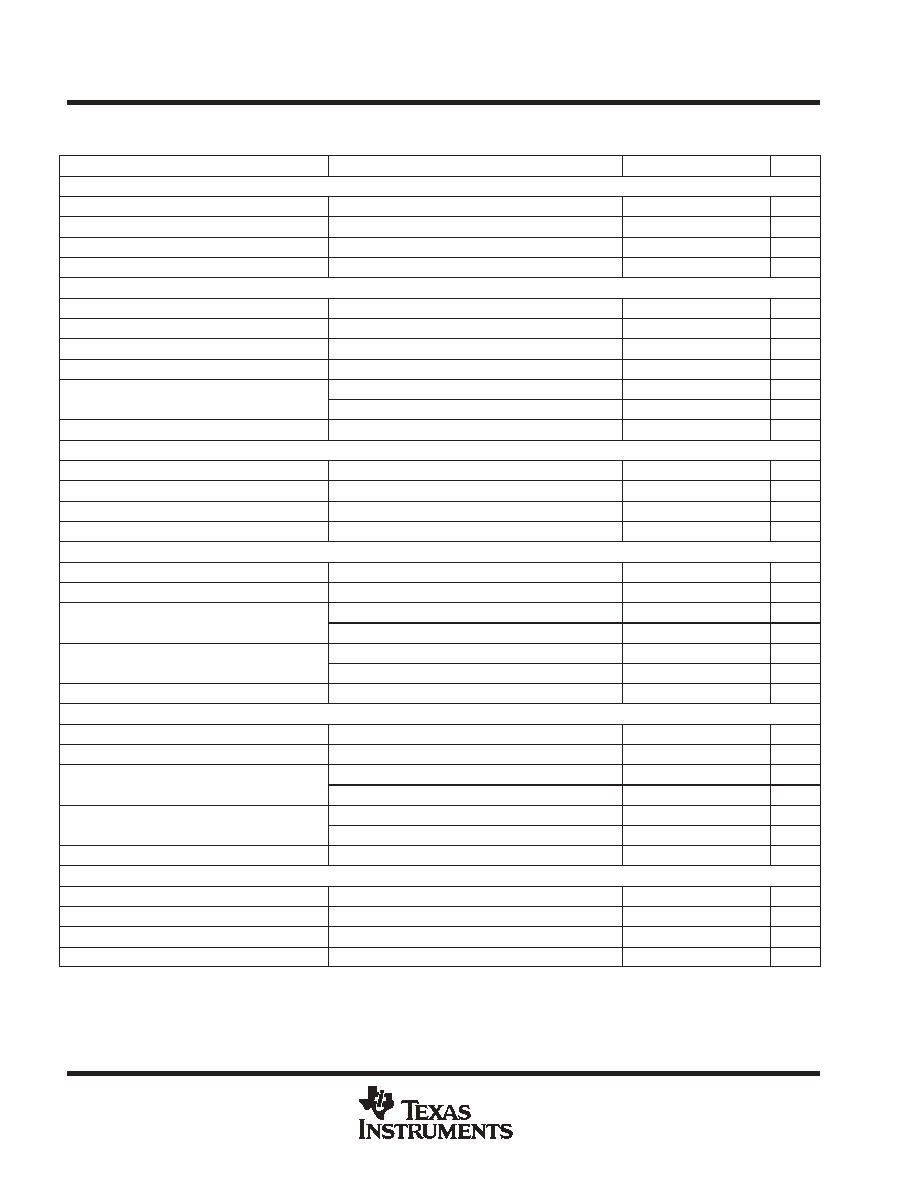
electrical characteristics over recommended operating free-air temperature range, T
A
= -40
∞
C to
85
∞
C for the UCC2942x, 0
∞
C to 70
∞
C for the UCC3942x, R
T
= 100 k
, V
VPUMP
= 6 V, V
VIN
= 3 V.
PARAMETER
TEST CONDITIONS
MIN
TYP
MAX
UNITS
Current Sense Section
Gain
8
10
11
V/V
Overcurrent limit threshold
120
150
190
mV
Unity gain bandwidth
See Note 1
25
MHz
COMP voltage to ISENSE accuracy
ISENSE = 70 mV
0.83
1.00
1.23
V
PWM Section
Maximum duty cycle
VISENSE = 0 V,
VFB = 0 V
80
88
%
Minimum duty cycle
VFB = 1.5 V
0
%
Low power mode VCOMP threshold
At COMP pin
0.53
0.60
0.67
V
Slope compensation accuracy
RT = 350 k
,
RSLOPE = 20 k
1.4
2.8
4.0
A/s
Rectifier zero current threshold
RSEL = GND
≠2
15
30
mV
Rectifier zero current threshold
RSEL = VIN
≠28
≠15
2
mV
RSEL threshold
0.5
0.9
1.3
V
PFM Section
PFM disable threshold
0.17
0.22
0.27
V
Comp hold during sleep
VPFM = 0.4 V
0.40
0.47
0.65
V
Startup delay after sleep
VFB < 1.23 V
4
9
µ
s
FB voltage to sleep off
1.185
1.220
1.245
V
VGSW Drive Section
Rise time
CO = 1 nF
18
35
ns
Fall time
CO = 1 nF
14
30
ns
Output high
IOUT = ≠100 mA,
Respect to VPUMP
0.4
0.65
V
Output high
IOUT = ≠1 mA,
Respect to VPUMP
4
10
mV
Output low
IOUT = 100 mA
0.2
0.35
V
Output low
IOUT = 1 mA
2
6
mV
Charge off to rectifier on delay
10
40
65
ns
RECT Drive Section
Rise time
CO = 1 nF
20
40
ns
Fall time
CO = 1 nF
14
30
ns
Output high
IOUT = ≠100 mA,
Respect to VPUMP
0.2
0.5
V
Output high
IOUT = ≠1 mA,
Respect to VPUMP
5
10
mV
Output low rectifier
IOUT = 100 mA
0.2
0.35
V
Output low rectifier
IOUT = 1 mA
2
6
mV
Rectifier off to charge on delay
10
40
65
ns
RESET Section (UCC39422 Only)
Reset timeout
CRSADJ = 0.33
µ
F
100
250
400
ms
Reset threshold
Percentage below regulation voltage
≠7
≠5.5
≠4
%
Output low voltage
Reset condition,
I = 5 mA
0.1
0.25
V
Output leakage
RESET = 8 V
0.05
0.2
µ
A
NOTE 1: Ensured by design. Not production tested.
UCC29421, UCC29422, UCC39421, UCC39422
MULTIMODE HIGH FREQUENCY PWM CONTROLLER
SLUS246C - OCTOBER 1999 - REVISED FEBRUARY 2005
5
POST OFFICE BOX 655303
∑
DALLAS, TEXAS 75265
electrical characteristics over recommended operating free-air temperature range, T
A
= -40
∞
C to
85
∞
C for the UCC2942x, 0
∞
C to 70
∞
C for the UCC3942x, R
T
= 100 k
, V
VPUMP
= 6 V, V
VIN
= 3 V.
PARAMETER
TEST CONDITIONS
MIN
TYP
MAX
UNITS
Voltage Detection Section (UCC39422 Only)
Threshold voltage
1.18
1.26
1.34
V
Output low voltage
I = 5 mA
0.15
0.3
V
Output leakage
LOWBAT = 8 V
0.05
0.25
µ
A
PIN DESCRIPTIONS
COMP: This is the output of the transconductance error amplifier. Connect the compensation components from
this pin to ground.
CHRG: This is the gate drive output for the N-channel charge MOSFET. Connect it to the gate directly, or through
a low-value gate resistor.
CP: This is the input for the charge pump. For applications requiring a charge pump, connect this pin to the
charge pump diode and flying capacitor, as shown in the applications diagram of Figure 4. For applications
where no charge pump is required, this pin should be grounded.
FB: The feedback input is the inverting input to the transconductance error amplifier. Connect this pin to a
resistive divider between V
OUT
and ground. The output voltage is regulated to:
V
OUT
+
1.235
(R1
)
R2)
R1
where R1 goes to GND and R2 goes to VOUT.
GND: This is the signal ground pin for the device. It should be tied to the local ground plane.
ISENSE: This is the input to the X10 wide bandwidth current-sense amplifier. Connect this pin to the high side
of the current-sense resistor. An internal current is sourced out this pin for slope compensation. For applications
requiring slope compensation (or filtering of the current-sense signal), use a resistor in series with this pin.
LOWBAT: This is the open drain output of the uncommitted comparator. (UCC39422 only). This output is low
when the VDET pin is above 1.25 V.
PFM: This is the programming pin for the PFM (pulse frequency modulation) mode threshold. Connect this pin
to a resistive divider off of the FB pin (or VOUT) to set the PFM threshold. To disable PFM Mode, connect this
pin to ground (below 0.2 V).
PGND: This is the power ground pin for the device. Connect it directly to the ground return of the current-sense
resistor.
RECT: This is the gate drive output for the synchronous rectifier. Connect it to the gate of the P- or N-channel
MOSFET directly, or through a low value gate resistor.
RSEN: This pin is used to sense the voltage across the synchronous rectifier for commutation. In boost
configurations, connect this pin through a 1-k
resistor to the junction of the two MOSFETs and the inductor.
In flyback and SEPIC configurations, connect this pin through a 1-k
resistor to the junction of the drain of the
synchronous rectifier and the secondary side winding of the coupled inductor.
RSADJ: A capacitor from this pin to ground sets the reset delay. (UCC39422 only)
RSEL: This pin programs the device for N- or P-channel synchronous rectifiers by inverting the phase of the
RECT gate drive output. Connect this pin to ground for N-channel MOSFETs, connect it to V
IN
for P-channel
MOSFETs.

UCC29421, UCC29422, UCC39421, UCC39422
MULTIMODE HIGH FREQUENCY PWM CONTROLLER
SLUS246C - OCTOBER 1999 - REVISED FEBRUARY 2005
6
POST OFFICE BOX 655303
∑
DALLAS, TEXAS 75265
RESET: This is the open drain output of the reset comparator. (UCC39422 only) and is active low.
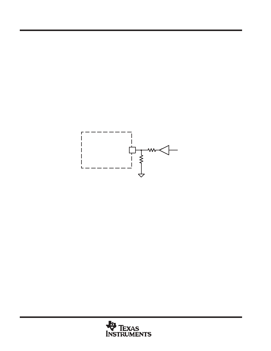
RT: A resistor from this pin to ground programs the frequency of the pulse width modulator.
Frequency (MHz)
^
50
R
T
(k
W
)
SYNC/SD: This pin has two functions. It may be used to synchronize the UCC39421's switching frequency to
an external clock, or to shutdown the IC entirely. In shutdown, the quiescent current is reduced to just a few
microamps (both external FETs are turned off). To shutdown the converter, this pin must be held high (above
2.0 V) for a minimum of 29
µ
s. If not used, this pin should be grounded.
To synchronize the internal oscillator to an external source, the SYNC/SD pin must be driven with a clock pulse,
with a minimum amplitude of 2.0 V. The internal circuitry syncs to the rising edge of the external clock. The clock
pulse width is not critical (must be 50 ns minimum).
Note: When coming out of shutdown (or during power-up), the SYNC/SD pin must be held low for a minimum
of 200
µ
s before applying an external clock to ensure startup.
VPUMP: This is the output of the charge pump. For applications requiring a charge pump, connect a 1-
µ
F
capacitor from this pin to ground. Otherwise, connect this pin to the higher of V
IN
or V
OUT
, and decouple with
a 0.1-
µ
F capacitor.
VOUT: Connect this pin to the output voltage. This input is used for sensing the voltage across the synchronous
rectifier and for supplying power to internal circuitry and should be decoupled with a 0.1-
µ
F capacitor.
VIN: This is the input power pin of the device. Connect this pin to the input voltage source. A 0.1-
µ
F decoupling
capacitor should be connected between this pin and ground.
VDET: This is the non-inverting input to an uncommitted comparator. This input may be used for detecting a
low-battery condition. (UCC39422 only)
UCC29421, UCC29422, UCC39421, UCC39422
MULTIMODE HIGH FREQUENCY PWM CONTROLLER
SLUS246C - OCTOBER 1999 - REVISED FEBRUARY 2005
7
POST OFFICE BOX 655303
∑
DALLAS, TEXAS 75265
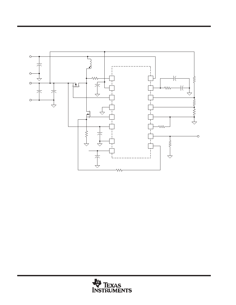
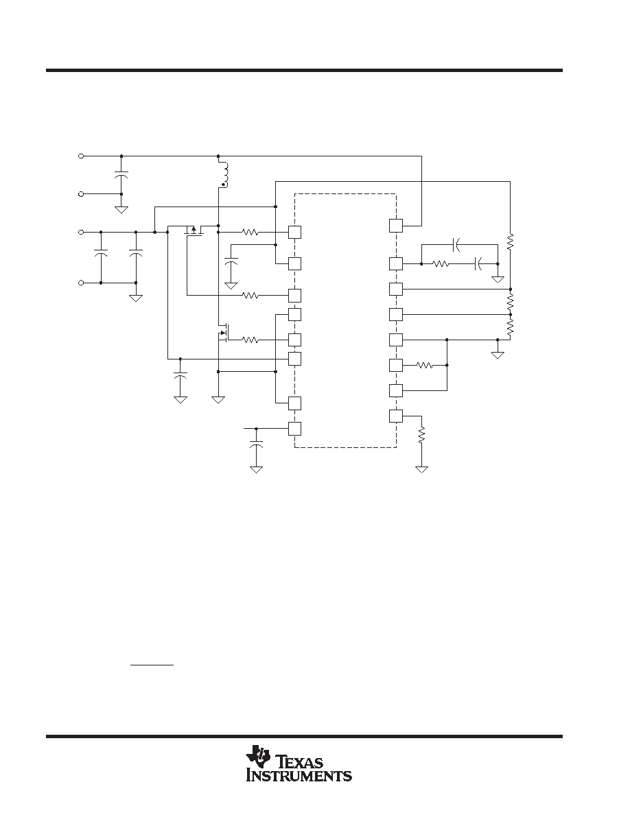
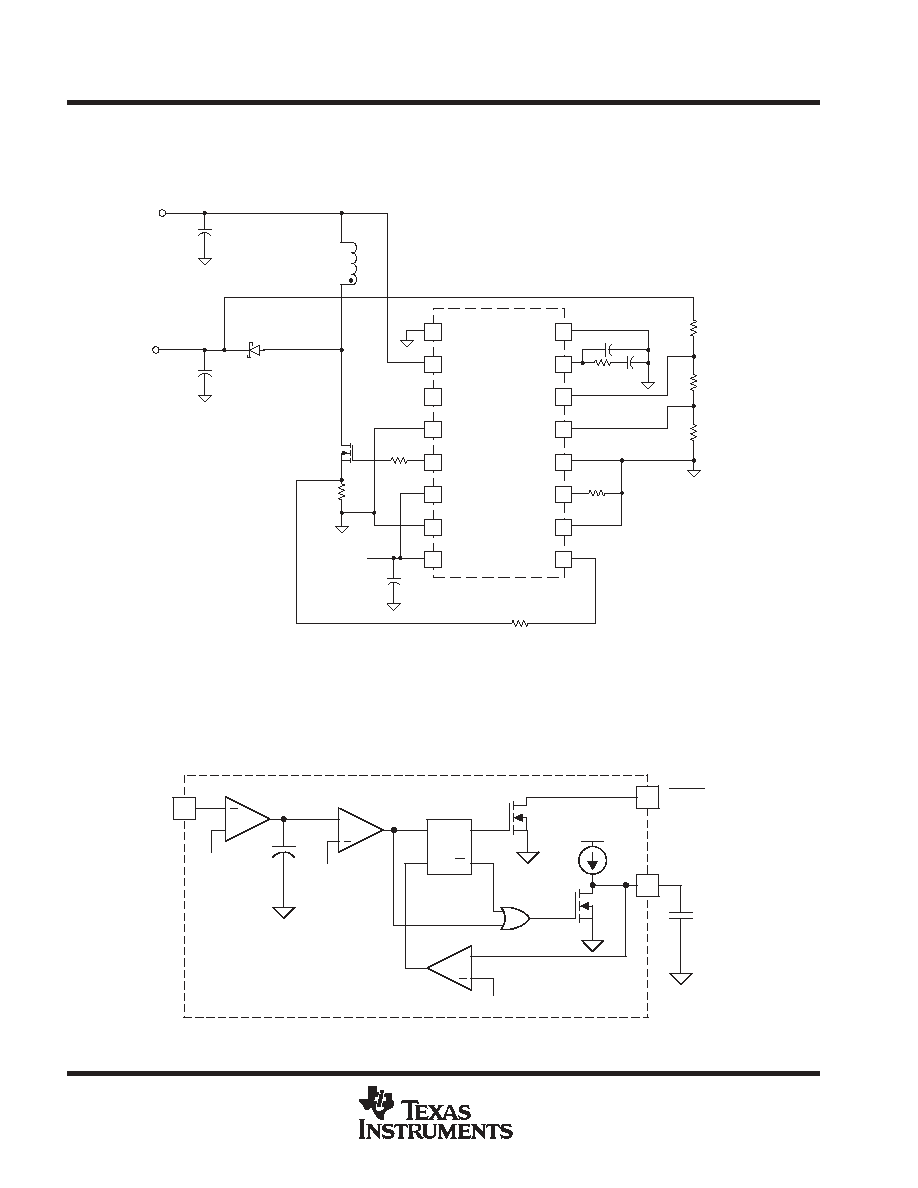
APPLICATION INFORMATION
The UCC39421 is a high frequency, synchronous PWM controller optimized for portable, battery-powered
applications where size and efficiency are of critical importance. It includes high-speed, high-current FET
drivers for those converter applications requiring low Rds(on) external MOSFETs. A detailed block diagram is
shown in Figure 2.
optimizing efficiency
The UCC39421 optimizes efficiency and extends battery life with its low quiescent current and its synchronous
rectifier topology. The additional features of low-power (LP) mode and PFM mode maintain high efficiency over
a wide range of load current. These features are discussed in detail.
power saving modes
Since this is a peak current mode controller, the error amplifier output voltage sets the peak inductor current
required to sustain the load. The UCC39421 incorporates two special modes of operation designed to optimize
efficiency over a wide range of load current. This is done by comparing the error amplifier output voltage (on
the COMP pin) to two fixed thresholds (one of which is user programmable). If the error amplifier output voltage
drops below the first threshold, low power mode is entered. If the error-amplifier output voltage drops even
further, below a second user programmable threshold, PFM mode is entered. These modes of operation are
designed to maintain high efficiency at light loads, and are described in detail in the following text. Refer to the
simplified block diagram of Figure 1 for the control logic.
UDG-98108
VOUT
SENSE
+
+
+
0.2 V
1.22
+
+
+
1=SLEEP
Q
S
R
HOLD AMP
70 mV
PFM
PFM COMP
+
PFM DISABLE COMP
ERROR AMP
1.24 V
0.6 V
LPM COMP
FB
COMP
PFM
1 = LP_MODE
Figure 1. Simplified Block Diagram of Low Power and Pulse Mode Control Logic
UCC29421, UCC29422, UCC39421, UCC39422
MULTIMODE HIGH FREQUENCY PWM CONTROLLER
SLUS246C - OCTOBER 1999 - REVISED FEBRUARY 2005
8
POST OFFICE BOX 655303
∑
DALLAS, TEXAS 75265
APPLICATION INFORMATION
power saving modes (continued)
UDG-98107
7
9
8
3
2
4
6
12
5
17
11
20
18
16
19
13
14
15
1
10
+
1.24 V
+
RESET/POR
+
UCC29422
ONLY
1.18 V
+
0.2 V
1.22
+
+
Q
S
R
+
+
70 mV
PFM
1=SLEEP
1.24 V
0.6 V
+
1.24 V
VREF
SLOPECOMP
+
PWM
OSC
VDD
CONTROL
VPUMP
VOUT
1.2 V
+
+
S
R
Q
Q
Q
R
S
2.5
µ
S
MUX
A
B
A/B
+
+
PFM DISABLE
COMP
ERROR AMP
PWM
COMP
1 = LP_MODE
ILIM COMP
LEB
0.3 V
30 MHz AMP
+
X10
0.15 V
VOUT>2.5 V
VPUMP >2.5 V
Q
Q
R
S
START-UP
36 mV
ANTI-
CROSS
COND.
VPUMP
1=SD
VIN
VOUT+2 V
VIN
IZERO
PGND
PUMP
SWITCH
CONTROL
VIN
VGD
CLK
SYNC/SD
RT
GND
LOWBAT
VDET
RSADJ
PFM
COMP
FB
PGND
ISENSE
CHRG
RSEL
RECT
RSEN
VOUT
CP
VIN
VPUMP
VDD BIAS
CONTROL
AND UVLO
VDD
ADAPTIVE
ZERO
CURRENT
SENSING
10%-20% OF FULL
LOAD = LP_MODE
85%
DMAX
VGD
RESET
VIN
+
PFM COMP
+
20
µ
s
DELAY
Figure 2. Detailed Block Diagram
UCC29421, UCC29422, UCC39421, UCC39422
MULTIMODE HIGH FREQUENCY PWM CONTROLLER
SLUS246C - OCTOBER 1999 - REVISED FEBRUARY 2005
9
POST OFFICE BOX 655303
∑
DALLAS, TEXAS 75265
APPLICATION INFORMATION
low power mode
During normal operation, at medium to high load currents, the switching frequency remains fixed, programmed
by the resistor on the RT pin. At these higher loads, the gate drive output on the CHRG pin (for the N-channel
charge FET) is the higher of V
IN
or V
PUMP
. When the load current drops (sensed by a drop in the error amp
voltage), the UCC39421 automatically enters LP mode, and the gate drive voltage on the CHRG pin is reduced
to lower gate drive losses. This helps to maintain high efficiency at light loads where the gate drive losses begin
to dominate and the lowest possible Rds(on) is not required. If the load increases, normal or "high power" mode
resumes. The expression for gate drive power loss is given by equation (1). It can be seen that the power varies
as a function of the applied gate voltage squared.
P
GATELOSS
+
Q
G
V
G
2
f
V
S
(1)
Where Q
G
is the total gate charge and V
S
is the gate voltage specified in the MOSFET manufacturer's data
sheet, V
G
is the applied gate drive voltage, and f is the switching frequency.
The nominal COMP voltage where LP mode is entered is 0.6 V. Given the internal offset and gain of the
current-sense amplifier, this corresponds to a peak switch current of:
I
PEAK
+
(0.6
*
0.3)
K
R
SENSE
+
0.03
R
SENSE
(2)
Where 0.6 V is the threshold for LP mode, 0.3 V is the internal offset, K is the nominal current-sense amplifier
gain of 10, and R
SENSE
is the value of the current-sense resistor. If the peak inductor current is below this value,
the UCC39421 enters LP mode and the gate drive voltage on the CHRG pin is equal to V
IN
. At peak currents
higher than this, the gate drive voltage is the higher of VIN or VPUMP.
PFM mode
At very light loads, the UCC39421 enters PFM mode. In this mode, when the error amplifier output voltage drops
below the PFM threshold, the controller goes into sleep mode until V
OUT
has dropped slightly (30 mV measured
at the feedback pin). At this time, the controller turns back on and operates at fixed frequency for a short duration
(typically a few hundred microseconds) until the output voltage has increased and the error amplifier output
voltage has dropped below the PFM threshold once again. Then the converter turns off and the cycle repeats.
This results in a very low duty cycle of operation, reducing all losses and greatly improving light load efficiency.
During sleep mode, most of the circuitry internal to the UCC39421 is powered down, reducing quiescent current
and maximizing efficiency.
The peak inductor current at which this mode is entered is user programmable by setting the voltage on the PFM
pin. This can be done with a single resistor in series with the feedback divider, as shown in the application
diagrams. The nominal peak current threshold for PFM mode is defined by the equation:
I
PEAK
^
1.25
R1
R1
)
R2
*
0.3
K
R
SENSE
(3)
UCC29421, UCC29422, UCC39421, UCC39422
MULTIMODE HIGH FREQUENCY PWM CONTROLLER
SLUS246C - OCTOBER 1999 - REVISED FEBRUARY 2005
10
POST OFFICE BOX 655303
∑
DALLAS, TEXAS 75265
APPLICATION INFORMATION
PFM mode (continued)
Where 0.3 V is the internal offset and K is the nominal current-sense amplifier gain of 10 and R
SENSE
is the value
of the current-sense resistor. Note that in this case, the PFM pin voltage is set by the R1/R2 resistive divider
off of the FB pin, which is regulated to 1.25 V.
During sleep mode, the COMP pin is forced to 70 mV above the PFM pin voltage. This minimizes error amplifier
overshoot when coming out of sleep mode, and prevents erroneously tripping the PFM comparator.
disabling PFM mode
The user may disable PFM mode by pulling the PFM pin below 0.2 V. In this case, the UCC39421 remains on,
in fixed frequency operation at all load currents. The PFM pin can also be driven, through a resistive divider,
off of an output from the system controller. This allows the system controller to prepare for an expected step
increase in load, improving the converter's large signal transient response. An example of this is shown in
Figure 3.
UCC39421
R2
R1
PFM
ENABLE OUTPUT
FROM CONTROLLER
7
Figure 3. Driving the PFM Pin From a Controller Output
choosing a topology and optimal synchronous rectifier
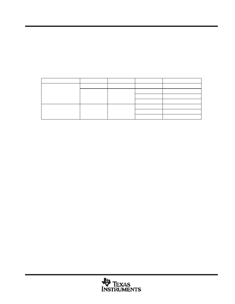
The UCC39421 is designed to be very flexible, and can be used in boost, flyback and SEPIC topologies. It can
operate from input voltages between 1.8 V and 8.0 V. Output voltages can be between 2.5 V and 8.0 V. It can
also drive either N- or P-channel MOSFET synchronous rectifiers. Table 1 can be used to select the appropriate
topology for a given combination of input and output voltage requirements. Although it is designed to operate
as a peak current mode controller, it can also be configured for voltage mode control. This is discussed in a later
section.
The user can program the gate drive output on the RECT pin for N-channel MOSFETs by grounding the RSEL
pin, or for P-channel MOSFETs by connecting the RESEL pin to VIN. Table 2 is used to determine whether an
N- or P-channel synchronous rectifier should be used.
Note: In all cases, low-voltage-logic MOSFETs should be used to achieve the lowest possible on-resistance
for the highest efficiency.
The application diagrams in Figures 4 through 8 illustrate the use of the UCC39421 in all the topologies, using
N- and P-channel rectifiers. They are be discussed in detail in the next section.
UCC29421, UCC29422, UCC39421, UCC39422
MULTIMODE HIGH FREQUENCY PWM CONTROLLER
SLUS246C - OCTOBER 1999 - REVISED FEBRUARY 2005
11
POST OFFICE BOX 655303
∑
DALLAS, TEXAS 75265
APPLICATION INFORMATION
choosing a topology and optimal synchronous rectifier (continued)
Note that the higher the frequency of operation, the more critical the MOSFET gate charge becomes for
efficiency, particularly at light loads. However, high load currents demand lower Rds(on), which tends to
increase gate charge. These two parameters should be balanced. At lower frequencies, the gate charge
becomes less important, at 1 MHz or more, it is critical.
Table 1. SELECTING TOPOLOGY BASED ON INPUT AND OUTPUT VOLTAGE REQUIREMENTS
Cell Type
Nunber of Cells
VIN Range
VOUT
Topology
2
1.8 V to 3.0 V
3.0 < V < 8.0
Boost
Alkaline or NiCd, NiMH
2.5 < V < 3.9
Flyback or SEPIC
Alkaline or NiCd, NiMH
3
2.7 V to 4.5 V
4.5 < V < 8.0
Boost
3
2.7 V to 4.5 V
V > 8.0
Non-synchronous boost
2.5 < V < 3.6
Flyback or SEPIC
Li-Ion
1
2.5 V to 4.2 V
4.2 < V < 8.0
Boost
Li-Ion
1
2.5 V to 4.2 V
V > 8.0
Non-synchronous boost
boost topology
The boost topology is simple and efficient, and should be used whenever the desired output voltage is greater
than the maximum input voltage.
boost using two n-channel MOSFETs
A boost converter using two N-channel MOSFETs is shown in Figure 4. This configuration is optimal for output
voltages below 4 V, where the output voltage may not be high enough to provide optimal gate drive for a
P-channel MOSFET. Note that in this case, a charge pump is required to provide proper gate drive levels. This
is easily accomplished by adding an external diode and a capacitor, as shown. The diode connects from the
output voltage to the CP pin. It should be an ultrafast or a Schottky diode. A 0.1-
µ
F ceramic capacitor is
connected from the drain of the charge FET to the CP pin. This is the "flying" capacitor that charges to (V
OUT
≠ V
DIODE
) every time the charge FET is on. A charge pump reservoir capacitor is connected from the VPUMP
pin to ground. It should be at least 1
µ
F. A high-speed active rectifier inside the UCC39421 charges the pump
capacitor from the CP pin. The charge pump voltage is:
V
PUMP
^
2
V
OUT
(4)
For a block diagram of the charge pump logic, refer to Figure 12.
Note: A charge pump should not be used at output voltages over 4.0 V to avoid pump voltages exceeding 8 V.
For other applications, where the charge pump is not required, the CP pin should be grounded and the pin
should be connected to either V
OUT
or V
IN
, whichever is greater.

UCC29421, UCC29422, UCC39421, UCC39422
MULTIMODE HIGH FREQUENCY PWM CONTROLLER
SLUS246C - OCTOBER 1999 - REVISED FEBRUARY 2005
12
POST OFFICE BOX 655303
∑
DALLAS, TEXAS 75265
APPLICATION INFORMATION
boost using two n-channel MOSFETs
UDG-98116
1
3
2
4
5
7
6
8
16
14
15
13
12
10
11
9
C5
0.1
µ
F
Q1
(N)
1k
0.1
µ
F
RSENSE
0.025
RSLOPE
1.5 k
ISENSE
VOUT
RSEN
VGRECT
PGND
CHRG
VPUMP
CP
VIN
RSEL
RT
GND
PFM
FB
COMP
SYNC/SD
UCC39421
CPOLE
RCOMP
CCOMP
RT
100 k
R1
20 k
1%
R2
41 k
1%
R3
100 k
1%
L1
COILTRONICS
CTX5-2
+CIN
100
µ
F
10 V
+1.8 V 3.2 V
+VIN
CPUMP1
µ
F
RG1
4.7
CFLY 0.1
µ
F
RG2 4.7
Q2 (N)
DPUMP
1N4148
COUT
+VIN
VOUT
+3.3 V
Figure 4. Application Diagram for the Boost Topology Using the N-channel Synchronous Rectifier
Table 2. SELECTING SYNCHRONOUS RECTIFIER BASED ON TOPOLOGY AND OUTPUT VOLTAGE
Topology
VOUT
Synchronous Rectifier
3.0 < V < 8.0
P-channel (low voltage logic)
Boost
V < 4.0
N-channel (low voltage logic)
Note: Requires a diode and a capacitor for the charge pump
Boost
V > 8.0
Non-synchronous
Note: Use Schottky rectifier (See Figure 16)
Flyback
2.5 < V < 3.0
N-channel (low voltage logic)
Note: Requires a diode and a capacitor for the charge pump
Flyback
3.0 < V < 8.0
N-channel (low voltage logic)
SEPIC
3.0 < V < 8.0
P-channel (low voltage logic)
UCC29421, UCC29422, UCC39421, UCC39422
MULTIMODE HIGH FREQUENCY PWM CONTROLLER
SLUS246C - OCTOBER 1999 - REVISED FEBRUARY 2005
13
POST OFFICE BOX 655303
∑
DALLAS, TEXAS 75265
APPLICATION INFORMATION
boost using N- and P-channel MOSFETs
For output voltages greater than the input and greater than about 3.0 V, a P-channel may be used for the
synchronous rectifier. This configuration is shown in Figure 5. In this case, the VPUMP pin should be connected
to VOUT. This configuration can be used for a 3.3 V output if a low voltage logic MOSFET is used.
relating peak inductor current to average output current for the boost converter
For a continuous mode boost converter, the average output current is related to the peak inductor current by
the following:
I
PEAK
+
I
OUT
(1
*
D)
)
di
2
(5)
where D is the duty cycle and the inductor ripple current, di, is defined as:
di
+
t
ON
V
IN
L
+
D
V
IN
f
L
(6)
where f is the switching frequency and L is the inductor value. The duty cycle is defined as:
D
+
V
O
*
V
IN
V
O
(7)
Substituting equations (6) and (7) into equation (5) yields:
I
PEAK
+
I
OUT
1
*
V
O
*
V
IN
V
O
)
V
IN
2
f
L
V
O
*
V
IN
V
O
(8)
Note that in these equations, the voltage drop across the rectifier has been neglected.
UCC29421, UCC29422, UCC39421, UCC39422
MULTIMODE HIGH FREQUENCY PWM CONTROLLER
SLUS246C - OCTOBER 1999 - REVISED FEBRUARY 2005
14
POST OFFICE BOX 655303
∑
DALLAS, TEXAS 75265
APPLICATION INFORMATION
relating peak inductor current to average output current for the boost converter
UDG-98117
1
3
2
4
5
7
6
8
16
14
15
13
12
10
11
9
C4
0.1
µ
F
C5
0.1
µ
F
Q1A
Si6803
(N)
R7
1 k
C6
0.1
µ
F
R
S
0.025
R6
1.5 k
ISENSE
VOUT
RSEN
VGRECT
PGND
CHRG
VPUMP
CP
VIN
RSEL
RT
GND
PFM
FB
COMP
SYNC/SD
UCC39421
C1
10 pF
R4
100 k
C2
470 pF
R4
100 k
R3
15 k
1%
R2
15 k
1%
R1
15 k
1%
R5
1 M
SYNC/
SHUDOWN
INPUT
L1
2.2
µ
H
Q1B
Si6803
(P)
C
OUT1
10
µ
F
16V
C
OUT2
10
µ
F
16V
+5 V
0 A
TO
1 A
C
IN1
10
µ
F
16V
V
IN
1.8 V
TO
4.8 V
+V
IN
Figure 5. Application Diagram for the Boost Topology Using a P-channel Synchronous Rectifier
flyback topology using n-channel MOSFETs
A flyback converter using the UCC39421 is shown in Figure 6. It uses a standard two-winding coupled inductor
with a 1:1 turns ratio. The advantage of this topology is that the output voltage can be greater or less than the
input voltage, as shown in Table 1. For example, this is ideal for generating 3.3 V from a Lithium-Ion cell. Note
that RC snubbers are placed across the primary and secondary windings to reduce ringing due to leakage
inductance. These are optional, and may not be required in the application.
Note that for converters where V
IN
and V
OUT
may both be below 3 V, a charge pump is needed to provide
adequate gate drive. This is illustrated in the example if Figure 7.

UCC29421, UCC29422, UCC39421, UCC39422
MULTIMODE HIGH FREQUENCY PWM CONTROLLER
SLUS246C - OCTOBER 1999 - REVISED FEBRUARY 2005
15
POST OFFICE BOX 655303
∑
DALLAS, TEXAS 75265
APPLICATION INFORMATION
flyback topology using n-channel MOSFETs (continued)
UDG-98113
1
3
2
4
5
7
6
8
16
14
15
13
12
10
11
9
C5
0.1
µ
F
Q1B
Si9802
(N)
1 k
0.1
µ
F
R
SENSE
0.05
R
SLOPE
1.5 k
ISENSE
VOUT
RSEN
VGRECT
PGND
CHRG
VPUMP
CP
VIN
RSEL
RT
GND
PFM
FB
COMP
SYNC/SD
UCC39421
C
POLE
R
COMP
C
COMP
RT
100 k
R1
20 k
1%
R2
41 k
1%
R3
100 k
1%
L1A
COILTRONICS
CTX5-2
C
IN
100
µ
F
10 V
2.5 V TO 8.0 V
+V
IN
RG1
4.7
RG2 4.7
C
OUT
V
IN
V
OUT
3.3 V
0.1
µ
F
Q1A
Si9802
(N)
L1B
10
470 pF
10
470 pF
+
+
Figure 6. Application Diagram for the Flyback Topology Using the N-channel Synchronous Rectifier

UCC29421, UCC29422, UCC39421, UCC39422
MULTIMODE HIGH FREQUENCY PWM CONTROLLER
SLUS246C - OCTOBER 1999 - REVISED FEBRUARY 2005
16
POST OFFICE BOX 655303
∑
DALLAS, TEXAS 75265
APPLICATION INFORMATION
flyback topology using n-channel MOSFETs (continued)
1
3
2
4
5
7
6
8
16
14
15
13
12
10
11
9
0.1
µ
F
Q1B
Si9802
(N)
1 k
0.1
µ
F
R
SENSE
0.05
R
SLOPE
1.5 k
ISENSE
VOUT
RSEN
VGRECT
PGND
CHRG
VPUMP
CP
VIN
RSEL
RT
GND
PFM
FB
COMP
SYNC/SD
UCC39421
C
POLE
R
COMP
C
COMP
RT
100 k
R1
20 k
1%
R2
41 k
1%
R3
100 k
1%
L1A
COILTRONICS
CTX5-2
C
IN
100
µ
F
10V
+1.8 V TO 4.2 V
+V
IN
RG1
4.7
RG2 4.7
C
OUT
V
IN
V
OUT
2.5 V
0.1
µ
F
Q1A
Si9802
(N)
L1B
10
470 pF
+
+
R
BIAS
180 k
D1
1N4148
UDG-98211
Figure 7. Flyback Converter Using Charge Pump Input for Low Voltage Operation
relating peak inductor current to average output current for the flyback converter
For a continuous mode flyback converter, the average output current is related to the peak inductor current by
the following:
I
PEAK
+
I
OUT
(1
*
D)
)
di
2
(9)
where D is the duty cycle and the inductor ripple current, dI, is defined as:
di
+
t
ON
V
IN
L
+
D
V
IN
f
L
(10)
where f is the switching frequency and L is the inductor value. The duty cycle is defined as:
UCC29421, UCC29422, UCC39421, UCC39422
MULTIMODE HIGH FREQUENCY PWM CONTROLLER
SLUS246C - OCTOBER 1999 - REVISED FEBRUARY 2005
17
POST OFFICE BOX 655303
∑
DALLAS, TEXAS 75265
APPLICATION INFORMATION
relating peak inductor current to average output current for the flyback converter (continued)
D
+
V
O
V
IN
)
V
O
(11)
Substituting equations (10) and (11) into equation (9) yields:
I
PEAK
+
I
OUT
1
*
V
O
V
IN
)
V
O
)
V
IN
2
f
L
V
O
V
IN
)
V
O
(12)
Figure 7 shows an example of a converter where both V
IN
and V
OUT
may be quite low in voltage. In this case,
a diode has been added to peak detect the voltage on the drain of the charge FET and use it for the pump input
voltage. This is used to drive the gates of the FETs. To assure that the pump voltage is used (rather than V
IN
,
which may be low), resistor R
BIAS
has also been added to the ISENSE input to inhibit LP mode. This technique
is discussed further in the section Changing the Low Power Threshold.
UDG-98214
1
3
2
4
5
7
6
8
16
14
15
13
12
10
11
9
0.1
µ
F
Q1
Si9802
(N)
1k
0.1
µ
F
R
SENSE
0.05
R
SLOPE
1.5k
ISENSE
VOUT
RSEN
VGRECT
PGND
CHRG
VPUMP
CP
VIN
RSEL
RT
GND
PFM
FB
COMP
SYNC/SD
UCC39421
C
POLE
R
COMP
C
COMP
RT
47k
R1
20k
1%
R2
41k
1%
R3
100k
1%
+V
IN
10
µ
F
10V
V
OUT
3.3V
L1B
+
1M
SYNC
INPUT
0.1
µ
F
L1A
C
IN
100
µ
F
10V
1.8 TO 6.0V
V
IN
+
Q2
(P)
10
µ
F 16V
Figure 8. Application Diagram for the SEPIC Technology Using a P-channel Synchronous Rectifier
UCC29421, UCC29422, UCC39421, UCC39422
MULTIMODE HIGH FREQUENCY PWM CONTROLLER
SLUS246C - OCTOBER 1999 - REVISED FEBRUARY 2005
18
POST OFFICE BOX 655303
∑
DALLAS, TEXAS 75265
APPLICATION INFORMATION
SEPIC topology using N- and P-channel MOSFETs
The UCC39421 may also be used in the SEPIC (single-ended primary inductance converter) topology. This
topology, which is similar to the flyback, uses a capacitor to aid in energy transfer from input to output. This
configuration is shown in Figure 8. The N
-
channel synchronous rectifier has been changed to a P-channel and
moved to the other end of the inductor's secondary winding, and a new capacitor has been placed across the
dotted ends of the two windings. The SEPIC topology offers the same advantage of the flyback in that it can
generate an output voltage that is greater or less than the input voltage.
However, it also offers improved efficiency. Although it requires an additional capacitor in the power stage, it
greatly reduces ripple current in the input capacitor and improves efficiency by transferring the energy in the
leakage inductance of the coupled inductor to the output. This also provides snubbing for the primary and
secondary windings, eliminating the need for RC snubbers. Note that the capacitor must have low ESR, with
sufficient ripple current rating for the application. Another advantage of the SEPIC is that the inductors do not
have to be on the same core.
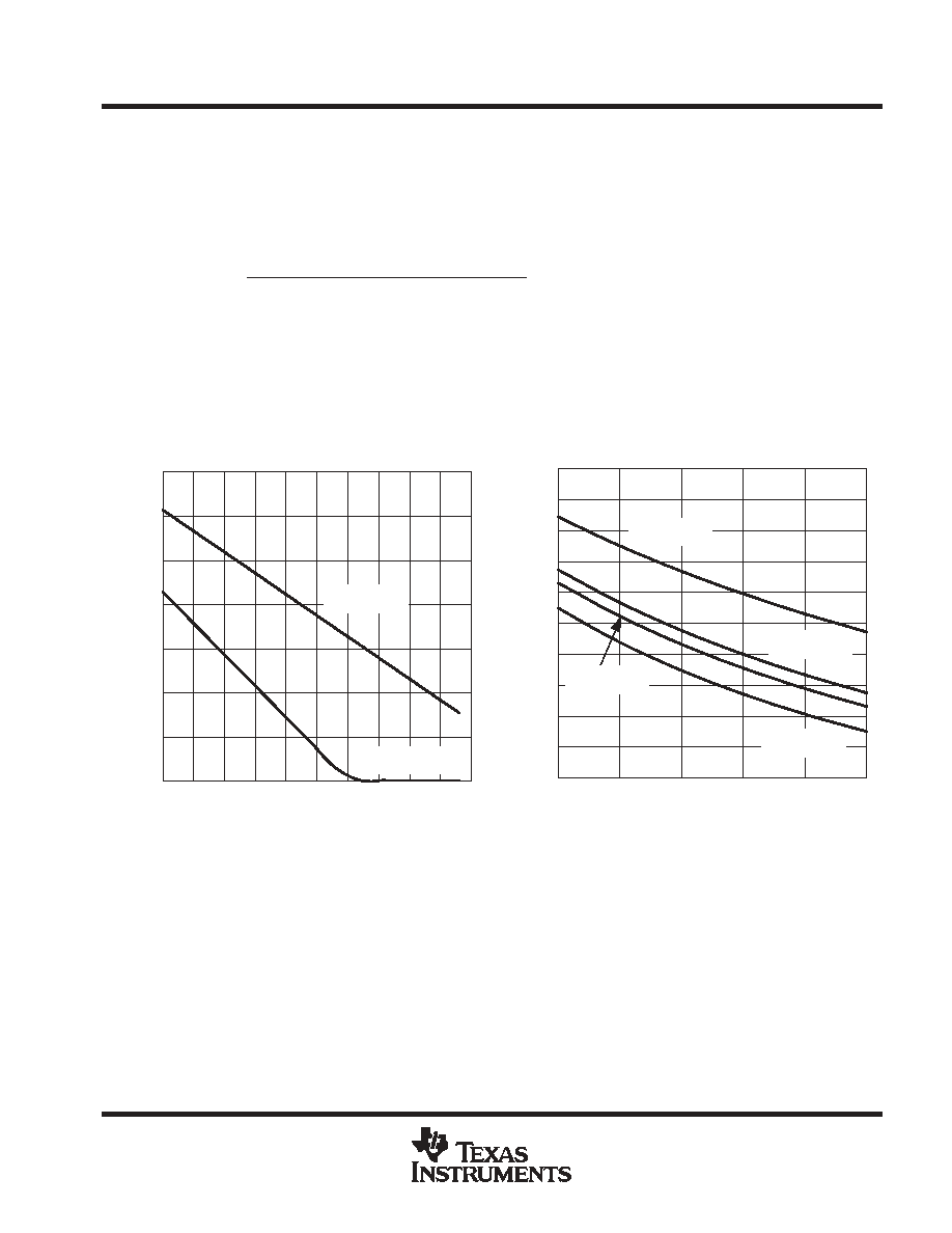
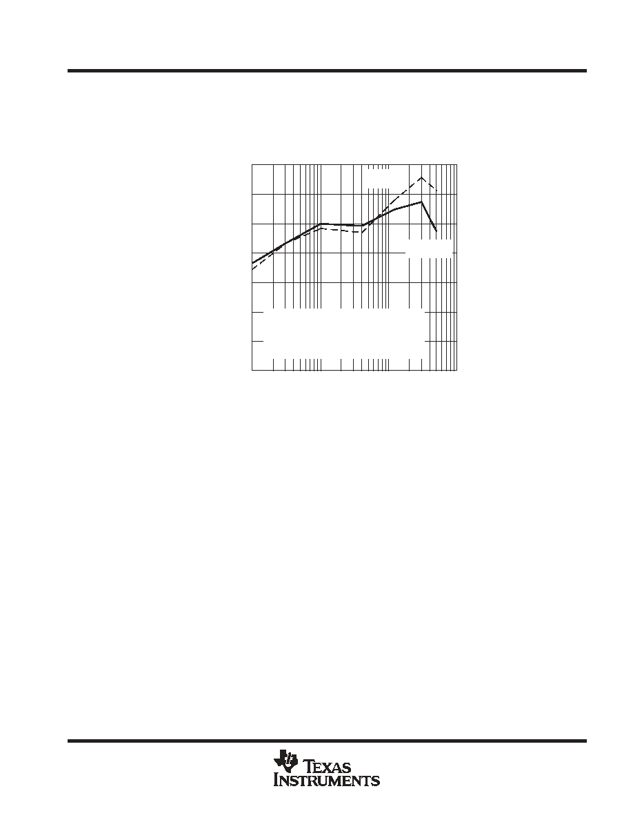
PWM duty cycle and slope compensation
All boost and flyback converters using peak current mode control are susceptible to a phenomenon known as
subharmonic oscillation when operated in the continuous conduction mode beyond 50% duty cycle. Continuous
conduction mode (CCM) means that the inductor current never goes to zero during the switching cycle. For a
CCM boost converter, the required duty cycle for a given input and output voltage (neglecting voltage drops
across the MOSFET switches) is given by equation (7). This is shown graphically for a number of common
output voltages in Figure 9. For example, it can be seen that for a 3.3-V output (using the boost topology) slope
compensation is not required because the duty cycle never exceeds 50%.
For the flyback topology, using a coupled inductor with a 1:1 turns ratio, the duty cycle is defined by
equation (11). This is shown graphically for a number of common output voltages in Figure 10.
To prevent subharmonic oscillation beyond 50% duty cycle, a technique called slope compensation is used,
which modifies the slope of the current ramp. This is accomplished by adding a part of the timing ramp to the
current-sense input. In the UCC39421, this can be done by simply adding a resistor in series with the ISENSE
input. A current is sourced within the IC which is proportional to the internal timing ramp voltage. The value of
the resistor determines the amount of slope compensation added.
The slope compensation output current at the ISENSE pin is equal to:
I
SLOPE
+
1
R
T
A
m
sec
(13)
where RT is the timing resister in ohms (
).
The required slope compensation resistor for a boost configuration is given by the equation:
R
SLOPE
+
V
OUT
*
2
V
IN min
R
SENSE
R
T
L
(14)
where R
SENSE
is the current-sense resistor value in ohms (
) and L is the inductor value in microhenries (
µ
H).
UCC29421, UCC29422, UCC39421, UCC39422
MULTIMODE HIGH FREQUENCY PWM CONTROLLER
SLUS246C - OCTOBER 1999 - REVISED FEBRUARY 2005
19
POST OFFICE BOX 655303
∑
DALLAS, TEXAS 75265
APPLICATION INFORMATION
PWM duty cycle and slope compensation (continued)
For a flyback topology, using a 1:1 turns ratio, the equation becomes:
R
SLOPE
+
V
OUT
*
V
IN min
R
SENSE
R
T
L
15)
If the converter is operated in the discontinuous conduction mode (inductor current drops to zero), no slope
compensation is required. The point at which this mode boundary occurs is a function of switching frequency,
input voltage, output voltage, load current, and inductor value. However, in general the converter is more
efficient when operated in the continuous conduction mode due to the lower peak currents.
Figure 9
CCM BOOST CONVERTER DUTY CYCLE
vs
INPUT VOLTAGE
2
0%
10%
20%
30%
40%
50%
60%
70%
3
4
V
OUT
= 5 V
V
OUT
= 3.3 V
Duty Cycle
VIN - Input Voltage - V
30%
V
OUT
= 2.5 V
V
OUT
= 3.3 V
V
OUT
= 5.0 V
40%
50%
60%
70%
80%
2
3
4
2.5
3.5
4.5
V
OUT
= 3.0 V
Figure 10
CCM FLYBACK CONVERTER DUTY CYCLE
vs
INPUT VOLTAGE
Duty Cycle
VIN - Input Voltage - V
voltage mode control
The UCC39421 can be operated as a voltage mode controller by connecting a 5.6-k
resistor from the ISENSE
pin to ground. The internal current source generates an artificial ramp voltage on this input. In this case, no slope
compensation is required, and no current-sense resistor is required in series with the source of the N-channel
MOSFET. A typical application diagram is shown in Figure 11. However, in this configuration there is no
overcurrent protection. In addition, the pulse and low power modes, designed to increase efficiency at light
loads, operates at different load currents. This is because the internal error amplifier's output voltage is no longer
a direct function of load current, but rather of duty cycle. When operating in CCM, the duty cycle is largely a
function of input and output voltage, not load current. At light enough loads however, the converter goes into
discontinuous mode and the error amplifier voltage drops low enough to activate the low power and pulse
modes.
UCC29421, UCC29422, UCC39421, UCC39422
MULTIMODE HIGH FREQUENCY PWM CONTROLLER
SLUS246C - OCTOBER 1999 - REVISED FEBRUARY 2005
20
POST OFFICE BOX 655303
∑
DALLAS, TEXAS 75265
APPLICATION INFORMATION
voltage mode control (continued)
UDG-98215
1
3
2
4
5
7
6
8
16
14
15
13
12
10
11
9
0.1
µ
F
Q1
(N)
1 k
0.1
µ
F
R
SLOPE
5.6 k
ISENSE
VOUT
RSEN
VGRECT
PGND
CHRG
VPUMP
CP
VIN
RSEL
RT
GND
PFM
FB
COMP
SYNC/SD
UCC39421
C
POLE
R
COMP
C
COMP
RT
100 k
R1
20 k
1%
R2
41 k
1%
R3
100 k
1%
+V
IN
0.1
µ
F
10V
V
OUT
5.0 V
L1
C
IN
100
µ
F
10V
1.8 V TO 4.5 V
V
IN
+
Q2
(P)
RG2
4.7
0.1
µ
F
RG1
4.7
C
OUT
+
Figure 11. Typical Boost Configuration Using Voltage Mode Control
start up
The UCC39421 incorporates a unique feature to help it start-up at low input voltages. If the input voltage is below
2.5 V at start-up, a separate control circuit takes over until V
OUT
or V
PUMP
gets above 2.5 V. In this mode, the
charge MOSFET is turned on for 5
µ
s, or until the voltage on the ISENSE pin reaches 36 mV, whichever occurs
first. The charge MOSFET then remains off for a fixed time of 2.5
µ
s, and the body diode of the synchronous
rectifier MOSFET is used to supply current to the output. This cycle repeats until either V
OUT
or V
PUMP
exceeds
2.5 V. This results in constant off time control, with a minimum switching frequency of approximately 120 kHz.
During this low voltage start-up mode, all other internal circuitry is off, including the synchronous rectifier drive
and the slope compensation current source. The peak inductor current during this mode is limited to:
I
PEAK
+
0.036
R
SENSE
(16)
UCC29421, UCC29422, UCC39421, UCC39422
MULTIMODE HIGH FREQUENCY PWM CONTROLLER
SLUS246C - OCTOBER 1999 - REVISED FEBRUARY 2005
21
POST OFFICE BOX 655303
∑
DALLAS, TEXAS 75265
APPLICATION INFORMATION
start up (continued)
If input voltages below 2.5 V are expected, it is important to use a low voltage logic N-channel MOSFET (with
a threshold voltage around 1 V or less) to ensure start-up at full load.
A block diagram of the low voltage start-up logic is shown in Figure 12.
UDG-98121
DRIVER
5-
µ
sec
DELAY
2.5-
µ
sec
DELAY
MUX
VIN
VPUMP
2.5 V < VPUMP
LPM < VCOMP
NORMAL PWM
B
A
VOUT
VIN
2.5 V < VPUMP
2.5 V < VOUT
VPUMP
UCC39421
+
S
R
Q
Q
A/B
+
+
RSENSE
CFLY
COUT
CPUMP
L
DBODY
36 mV
-
-
Figure 12. Symplified Diagram of Low Voltage Start-Up and Charge Pump Control Logic
anticross-conduction and adaptive synchronous rectifier commutation logic
When operating in the continuous conduction mode (CCM), the charge MOSFET and the synchronous rectifier
MOSFET are simply driven out of phase, so that when one is on the other is off. There is a built-in time delay
of about 30 ns to prevent any cross-conduction.
In the event that the converter is operating in the discontinuous conduction mode (DCM), the synchronous
rectifier needs to be turned off sooner, when the rectifier current drops to zero. Otherwise, the output begins
to discharge as the current reverses and goes back through the rectifier to the input. (This obviously cannot
happen when using a conventional diode rectifier). To prevent this, the UCC39421 incorporates a high-speed
comparator that senses the voltage on the synchronous rectifier (using the RSEN input) for purposes of
commutation. In the boost and SEPIC topologies, the synchronous rectifier is turned off when the voltage on
the RSEN pin goes negative with respect to V
OUT
. For this reason, it is important to have the VOUT pin well
decoupled.
UCC29421, UCC29422, UCC39421, UCC39422
MULTIMODE HIGH FREQUENCY PWM CONTROLLER
SLUS246C - OCTOBER 1999 - REVISED FEBRUARY 2005
22
POST OFFICE BOX 655303
∑
DALLAS, TEXAS 75265
APPLICATION INFORMATION
anticross-conduction and adaptive synchronous rectifier commutation logic (continued)
In the flyback topology however (using a ground referenced N-channel MOSFET rectifier), the rectifier voltage
is sensed on the MOSFET drain, with respect to ground rather than V
OUT
. The voltage polarity in this case is
opposite that of the boost and SEPIC topologies. This problem is solved with the adaptive logic within the
UCC39421. During each charge cycle, while the N-channel charge FET is on, a latch is set if the voltage on the
RSEN pin exceeds V
IN
/2. This indicates a flyback topology, since this node is be equal to or greater than V
IN
at this time. In the case of the boost and the SEPIC, the voltage at the RSEN input is near or below ground, and
the latch is not be set. This allows the UCC39421 to sense which topology is in use and adapt the synchronous
rectifier commutation logic accordingly. Note that the RSEN input must have a series resistor to limit the current
when going below ground. Values less than or equal to 1 k
are recommended to prevent time delay due to
stray capacitance.
current-sense amplifier and leading edge blanking
The UCC39421 includes a high-speed current-sense amplifier with a nominal gain of 10 to minimize losses
associated with the current-sense resistor. The amplifier was designed to provide good response and minimal
propagation delay, allowing switching frequencies at 2 MHz. The current-sense resistor should be chosen to
provide a maximum peak voltage of 100 mV at full load, with the minimum input voltage.
A leading-edge blanking time of 40 ns is provided to filter out leading-edge spikes in the current-sense
waveform. In most applications, this eliminates the need for a filter capacitor on the ISENSE pin.
overcurrent protection
The UCC39421 includes a peak current limit function. If the voltage on the ISENSE pin exceeds 0.15 V after
the initial blanking period, the pulse is terminated and the charge MOSFET is turned off.
sync/shutdown input
The SYNC/SD pin has two functions; it may be used to synchronize the UCC39421's switching frequency to
an external clock, or to shutdown the IC entirely. In shutdown, the quiescent current is reduced to just a few
microamps.
To synchronize the internal clock to an external source, the SYNC/SD pin must be driven high, above 2.0 V
minimum. The circuitry syncs to the rising edge of the input, the pulse width is not critical.
To shutdown the converter, the SYNC/SD pin must be held high (above 2.0 V) for a minimum of 29
µ
s.
This pin should be grounded if not used.
changing the low power mode threshold
For some applications the user may want to lower the low power (LP) mode threshold, or even eliminate this
feature altogether. For example, if a boost topology is being used, and the input voltage is below 2.5 V, the gate
drive to the charge FET may want to be derived from the pump (or output) voltage under all load conditions,
rather than from V
IN
. This means the converter would never be allowed to operate in LP mode.

UCC29421, UCC29422, UCC39421, UCC39422
MULTIMODE HIGH FREQUENCY PWM CONTROLLER
SLUS246C - OCTOBER 1999 - REVISED FEBRUARY 2005
23
POST OFFICE BOX 655303
∑
DALLAS, TEXAS 75265
APPLICATION INFORMATION
changing the low power mode threshold (continued)
Although the LP mode threshold is internally fixed at 0.6 V (referenced to the pin), the point at which the LP
mode is entered can be easily modified by adding a single resistor, as shown in Figure 13. Resistor R
BIAS
forms
a divider with R
SLOPE
(used for slope compensation) and adds a dc offset to the current-sense input, raising
the output voltage of the sense amplifier and fooling the LP mode comparator into thinking the load is higher
than it is. The required bias resistor to transition out of LP mode for a given peak current can be calculated using
the following equation:
R
BIAS
+
R
SLOPE
V
OUT
0.03
*
I
PEAK
R
SENSE
(17)
UDG-98213
VOUT
COUT
+
300 mV
RSENSE
RSLOPE
RBIAS
+
DRIVE
CONTROL
LOGIC
+
LP MODE
+
X10
600 mV
PWM
COMP
FB
1.24 V
CHRG
ISENSE
17
18
6
12
UCC39421
VIN
Figure 13. Modifying Low Power (LP) Mode Threshold
Due to the current-sense amplifier gain of 10 and the internal offset of 300 mV, an offset of just 30 mV or more
at the ISENSE pin inhibits the LP mode altogether. Note that inhibiting LP mode does not prevent PFM from
working, as long as the PFM pin is set to a voltage higher than:
10
V
ISENSE
)
0.3V
18)
programming the PWM frequency
Some applications may want to remain in a fixed frequency mode of operation, even at light load, rather than
going into PFM mode. This lowers efficiency at light load. One way to improve the efficiency while maintaining
fixed frequency operation is to lower the PWM frequency under light load conditions. This can be easily done,
as shown in Figure 14. By adding a second timing resistor and a small MOSFET switch, the host can switch
between two discrete frequencies at any time.

UCC29421, UCC29422, UCC39421, UCC39422
MULTIMODE HIGH FREQUENCY PWM CONTROLLER
SLUS246C - OCTOBER 1999 - REVISED FEBRUARY 2005
24
POST OFFICE BOX 655303
∑
DALLAS, TEXAS 75265
APPLICATION INFORMATION
non-synchronous boost for higher output voltage applications
The UCC39421 can also be used in non-synchronous applications to provide output voltages greater than 8
volts from low voltage inputs. An example of a 12-V boost application is shown in Figure 16. Since none of the
IC pins are exposed to the boosted voltage, the output voltage is limited only by the ratings of the external
MOSFET, rectifier, and filter capacitor. At these higher output voltages, good efficiency is maintained since the
rectifier drop is small compared to the output voltage. Note that PFM mode can still be used to maintain high
efficiency at light load. Typical efficiency causes are shown in Figure 15.
Since all the power supply pins (VIN, VOUT, VPUMP) operate off the input voltage, it must be >2.5 V and high
enough to assure proper gate drive to the charge FET.
UDG-98216
1
3
2
4
5
7
6
8
16
14
15
13
12
10
11
9
ISENSE
VOUT
RSEN
VGRECT
PGND
CHRG
VPUMP
CP
VIN
RSEL
RT
GND
PFM
FB
COMP
SYNC/SD
UCC39421
R2
R1
VOUT
RT1
2N7002
RT2
FREQUENCY
CONTROL
Figure 14. Changing the PWM Frequency
UCC29421, UCC29422, UCC39421, UCC39422
MULTIMODE HIGH FREQUENCY PWM CONTROLLER
SLUS246C - OCTOBER 1999 - REVISED FEBRUARY 2005
25
POST OFFICE BOX 655303
∑
DALLAS, TEXAS 75265
APPLICATION INFORMATION
non-synchronous boost for higher output voltage applications (continued)
Figure 15
NON-SYNCHRONOUS BOOST EFFICIENCY
V
IN
= 5 V
V
IN
= 3.3 V
95%
90%
85%
80%
75%
70%
65%
60%
0.001
0.01
0.1
1
f = 550 kHz
L = 6.8 mH
DT3316P-682 (IRF7601) MBR0530
VPFM = 0.5 V
Efficiency
I
OUT
- Output Current - A
UCC29421, UCC29422, UCC39421, UCC39422
MULTIMODE HIGH FREQUENCY PWM CONTROLLER
SLUS246C - OCTOBER 1999 - REVISED FEBRUARY 2005
26
POST OFFICE BOX 655303
∑
DALLAS, TEXAS 75265
APPLICATION INFORMATION
non-synchronous boost for higher output voltage applications (continued)
UDG-98212
RT
100 K
RCOMPC
COMP
Q1
(N)
RG1
4.7
RSENSE
0.05
COUT
100
µ
F
16V
CIN
100
µ
F
16V
0.1
µ
F
+VIN
12V
R3
249 K
1%
R2
17.8 K
1%
R1
11 K
1%
+
+
RSLOPE
1.5 K
CPOLE
1.25 V
3.0 V TO 8.0V
L1
6.8
µ
H
1
2
3
4
5
6
7
10
9
8
UCC39421
16
15
14
13
12
11
ISENSE
VOUT
RSEN
VGRECT
PGND
VGCHRG
VPUMP
CP
VIN
RSEL
RT
GND
PFM
FB
COMP
SYNC/SD
D1
MBR0530T
N/C
Figure 16. Non-Synchronous Boost Converter for Higher Output Voltages
UCC39422 features
The UCC39422 is a 20-pin device that adds a reset function and an uncommitted comparator to the UCC39421.
A simplified diagram of the reset circuit is shown in Figure 17.
UDG-98206
17
20
1
RESET
RSADJ
S
Q
Q
R
1
µ
A
C RESET
+
+
8 pF
1.175 V
+
FB
g
m
=1/26 k
1.175 V
1.175 V
V
IN
Figure 17. Reset Circuitry
UCC29421, UCC29422, UCC39421, UCC39422
MULTIMODE HIGH FREQUENCY PWM CONTROLLER
SLUS246C - OCTOBER 1999 - REVISED FEBRUARY 2005
27
POST OFFICE BOX 655303
∑
DALLAS, TEXAS 75265
APPLICATION INFORMATION
The reset circuit monitors the voltage at the feedback (FB) pin and issues a reset if the feedback voltage drops
below 1.175 V. This represents a 6% drop in output voltage. Monitoring the voltage internally at the FB pin
eliminates the need for another external voltage divider. The RESET output is an open-drain output that is active
low during reset. It stays low until the feedback voltage is above 1.175 V for a period of time called the reset
pulse width, which is user programmable. An external capacitor on the RSADJ pin and an internal 1-
µ
A current
source determine the reset pulse width, according to the following equation:
t
RESET
+
C
RESET
1.18
(19)
where t
RESET
is the reset pulse width in seconds, and C
RESET
is the capacitor value in microFarads (
µ
F).
An adaptive glitch filter is included to prevent nuisance trips. This is implemented using a gm amplifier to charge
an 8-pF capacitor to 1.175 V before declaring a reset. This provides a delay which is inversely proportional to
the magnitude of the feedback voltage error. The delay time is approximated by the following equation:
t
DELAY
^
0.25
1.175
*
V
FB
m
s
(20)
where t
DELAY
is the filter delay time in microseconds. Note that the maximum current from the gm amplifier is
limited to 2
µ
A, limiting the minimum time delay to 4.8
µ
s.
A typical application schematic using the UCC39422 is shown in Figure 18. In this example, R1 and R2 have
been selected to trip the LOWBAT output when V
IN
drops below 2.0 V. Note that the RESET and LOWBAT
outputs are open drain and require a pullup.
UCC29421, UCC29422, UCC39421, UCC39422
MULTIMODE HIGH FREQUENCY PWM CONTROLLER
SLUS246C - OCTOBER 1999 - REVISED FEBRUARY 2005
28
POST OFFICE BOX 655303
∑
DALLAS, TEXAS 75265
APPLICATION INFORMATION
UCC39422 features (continued)
UDG-99034
2
4
3
5
6
8
7
9
19
17
18
16
15
13
14
12
1 k
0.1
µ
F
R
SLOPE
ISENSE
VOUT
RSEN
VGRECT
PGND
CHRG
VPUMP
CP
RSEL
RT
GND
PFM
FB
COMP
SYNC/SD
UCC39422
C
POLE
R
COMP
C
COMP
RT
100 k
L1
+C
IN
0.1
µ
F
RG
RG
+ C OUT
V
IN
+V
OUT
10
VIN
1
RESET* (ACTIVE LOW)
0.1
µ
F
R1
250 k
+V
IN
C
RESET
RSETB
Q1 (N)
R
SENSE
20
RSADJ
Q1 (P)
11
VDET
LOWBAT (ACTIVE HIGH)
47 pF
R2
150 k
THRESHOLD = 2.0 V
+V
IN
LOWBAT
Figure 18. Typical UCC39422 Application
UCC29421, UCC29422, UCC39421, UCC39422
MULTIMODE HIGH FREQUENCY PWM CONTROLLER
SLUS246C - OCTOBER 1999 - REVISED FEBRUARY 2005
29
POST OFFICE BOX 655303
∑
DALLAS, TEXAS 75265
APPLICATION INFORMATION
selecting the inductor
The inductor must be chosen based on the desired operating frequency and the maximum load current. Higher
frequencies allow the use of lower inductor values, reducing component size. Higher load currents require larger
inductors with higher current ratings and less winding resistance to minimize losses. The inductor must be rated
for operation at the highest anticipated peak current. Refer to equation (8) and equation (12) to calculate the
peak inductor current for a boost or flyback design, based on V
IN
, V
OUT
, maximum load, frequency, and inductor
value. Some manufacturers rate their parts for maximum energy storage in microjoules (
µ
J). This is expressed
by:
E
+
0.5
L
I
PEAK
2
(21)
where E is the required energy rating in microjoules. L is the inductor value in microhenries (
µ
H) (with current
applied), and I
PEAK
is the peak current in amps that the inductor sees in the application. Another way in which
inductor ratings are sometimes specified is the maximum volt-seconds applied. This is given simply by:
E
T
+
V
IN
D
f
(22)
where ET is the required rating in V-
µ
s, D is the duty cycle for a given V
IN
and V
OUT
, and f is the switching
frequency in MHz. Refer to equations (7) and (11) to calculate the duty cycle for a CCM boost or flyback
converter.
In any case, the inductor must use a low loss core designed for high-frequency operation. High-frequency ferrite
cores are recommended. Some manufacturers of off-the-shelf surface-mount designs are listed in Table 3. For
flyback and SEPIC topologies, use a two-winding coupled inductor. SEPIC designs can also use two discrete
inductors.
Table 3. MT COMMERCIAL INDUCTOR MANUFACTURERS
Coilcraft Inc.
(800) 322-2645.1102 Silver Lake RD, Cary, IL 60013
Coiltronics Inc.
(407) 241-7876 6000 Park of Commerce Blvd, Boca Raton, FL 33487
Dale Electronics, Inc.
(605) 665-9301East Highway 50, Yankton, SD 57078
Pulse Engineering Ltd.
(204) 633-4321300 Keewatin Street, Winnipeg, MB R2X 2R9
Sumida
Voice (65) 296-3388
Fax (65) 293-3390 Block 996, Bendemeer Rd., #04-05/06 Singapore 33944
BH Electronics
(612) 894-9590 12219 Wood Lake Drive, Burnsville, MN 55337
Tokin America Inc.
(408) 432-8020155 Nicholson Lane, San Jose CA 95134
UCC29421, UCC29422, UCC39421, UCC39422
MULTIMODE HIGH FREQUENCY PWM CONTROLLER
SLUS246C - OCTOBER 1999 - REVISED FEBRUARY 2005
30
POST OFFICE BOX 655303
∑
DALLAS, TEXAS 75265
APPLICATION INFORMATION
selecting the filter capacitor
The input and output filter capacitors must have low ESR and low ESL. Surface-mount tantalum, OSCONs or
multilayer ceramics (MLCs) are recommended. The capacitor selected must have the proper ripple current
rating for the application. Some recommended capacitor types are listed in Table 4.
Table 4. RECOMMENDED SMT FILTER CAPACITORS
Manufacturer
Part Number
Features
AVX
TPS series
Low ESR tantalum
Kemet
T410 series
Low ESR tantalum
Murata
GRM series
Low ESR ceramic
Sanyo
OSCON series
Low ESR organic
Sprague
591D series
Low ESR, low profile tantalum
Sprague
594D series
Low ESR tantalum
Tokin
Y5U, Y5V Type
Low ESR ceramic
Taiyo Yuden
X5R Type
Low ESR ceramic
circuit layout and grounding
As with any high frequency switching power supply, circuit layout, hookup, and grounding are critical for proper
operation. Although this may be a relatively low-power, low-voltage design, these issues are still very important.
The MOSFET turn-on and turn-off times necessary to maintain high efficiency at high switching frequencies of
1 MHz or more result in high dv/dt and di/dts. This makes stray circuit inductance especially critical. In addition,
the high impedances associated with low-power designs, such as in the feedback divider, make them especially
susceptible to noise pickup.
layout
The component layout should be as tight as possible to minimize stray inductance. This is especially true of the
high-current paths, such as in series with the MOSFETs and the input and output filter capacitors.
The components associated with the feedback, compensation and timing should be kept away from the power
components (MOSFETs, inductor). Keep all components as close to the IC pins as possible. Nodes that are
especially noise sensitive are the FB and RT pins. Other sensitive pins are COMP and PFM.
grounding
A ground plane is highly recommended. The PGND pin of the UCC39421 should be close to the grounded end
of the current-sense resistor, the input filter cap, and the output filter cap. The GND pin should be close to the
grounded end of the RT resistor, the feedback divider resistor, the ISENSE capacitor (if used), and the
compensation network.
MOSFET gate resistors
The UCC39421 includes low-impedance CMOS output drivers for the two external MOSFET switches. The
CHRG output has a nominal resistance of 4
, and the RECT has a nominal resistance of 2
. For
high-frequency operation using low gate charge MOSFETs, no gate resistors are required. To reduce
high-frequency ringing at the MOSFET gates, low-value series gate resistors may be added. These should be
non-inductive resistors, with a value of 2
to 10
, depending on the frequency of operation. Lower values
results in better switching times, improving efficiency.

UCC29421, UCC29422, UCC39421, UCC39422
MULTIMODE HIGH FREQUENCY PWM CONTROLLER
SLUS246C - OCTOBER 1999 - REVISED FEBRUARY 2005
31
POST OFFICE BOX 655303
∑
DALLAS, TEXAS 75265
APPLICATION INFORMATION
minimizing output ripple and noise spikes
The amount of output ripple is determined primarily by the type of output filter capacitor and how it is connected
in the circuit. In most cases, the ripple is be dominated by the ESR (equivalent series resistance) and ESL
(equivalent series inductance) of the capacitor, rather than the actual capacitance value. Low ESR and ESL
capacitors are mandatory in achieving low output ripple. Surface-mount packages greatly reduce the ESL of
the capacitor, minimizing noise spikes. To further minimize high frequency spikes, a surface mount ceramic
capacitor should be placed in parallel with the main filter capacitor. For best results, a capacitor should be
chosen whose self-resonant frequency is near the frequency of the noise spike. For high switching frequencies,
ceramic capacitors alone may be used, reducing size and cost.
For applications where the output ripple must be extremely low, a small LC filter may be added to the output.
The resonant frequency should be below the selected switching frequency, but above that of any dynamic loads.
The filter's resonant frequency is given by:
f
RES
+
1
2
p
L
C
(23)
Where f is the frequency in Hz, L is the filter inductor value in Henries, and C is the filter capacitor value in Farads.
It is important to select an inductor rated for the maximum load current and with minimal resistance to reduce
losses. The capacitor should be a low-impedance type, such as a tantalum.
If an LC ripple filter is used, the feedback point can be taken before or after the filter, as long as the filter's
resonant frequency is well above the loop crossover frequency. Otherwise, the additional phase lag makes the
loop unstable. The only advantage to connecting the feedback after the filter is that any small voltage drop
across the filter inductor is corrected for in the loop, providing the best possible voltage regulation. However,
the resistance of the inductor is usually low enough that the voltage drop is negligible.
PACKAGING INFORMATION
Orderable Device
Status
(1)
Package
Type
Package
Drawing
Pins Package
Qty
Eco Plan
(2)
Lead/Ball Finish
MSL Peak Temp
(3)
UCC29421N
ACTIVE
PDIP
N
16
20
None
CU SNPB
Level-NA-NA-NA
UCC29421PW
ACTIVE
TSSOP
PW
16
90
None
CU NIPDAU
Level-2-220C-1 YEAR
UCC29421PWTR
ACTIVE
TSSOP
PW
16
1
None
CU NIPDAU
Level-2-220C-1 YEAR
UCC29422N
ACTIVE
PDIP
N
20
18
None
CU SNPB
Level-NA-NA-NA
UCC29422PW
ACTIVE
TSSOP
PW
20
70
None
CU NIPDAU
Level-2-220C-1 YEAR
UCC29422PWTR
ACTIVE
TSSOP
PW
20
2000
None
CU NIPDAU
Level-2-220C-1 YEAR
UCC39421N
ACTIVE
PDIP
N
16
25
None
CU SNPB
Level-NA-NA-NA
UCC39421PW
ACTIVE
TSSOP
PW
16
90
None
CU NIPDAU
Level-2-220C-1 YEAR
UCC39421PWTR
ACTIVE
TSSOP
PW
16
2000
None
CU NIPDAU
Level-2-220C-1 YEAR
UCC39422N
ACTIVE
PDIP
N
20
18
None
CU SNPB
Level-NA-NA-NA
UCC39422PW
ACTIVE
TSSOP
PW
20
70
None
CU NIPDAU
Level-2-220C-1 YEAR
UCC39422PWTR
ACTIVE
TSSOP
PW
20
2000
None
CU NIPDAU
Level-2-220C-1 YEAR
(1)
The marketing status values are defined as follows:
ACTIVE: Product device recommended for new designs.
LIFEBUY: TI has announced that the device will be discontinued, and a lifetime-buy period is in effect.
NRND: Not recommended for new designs. Device is in production to support existing customers, but TI does not recommend using this part in
a new design.
PREVIEW: Device has been announced but is not in production. Samples may or may not be available.
OBSOLETE: TI has discontinued the production of the device.
(2)
Eco Plan - May not be currently available - please check
http://www.ti.com/productcontent
for the latest availability information and additional
product content details.
None: Not yet available Lead (Pb-Free).
Pb-Free (RoHS): TI's terms "Lead-Free" or "Pb-Free" mean semiconductor products that are compatible with the current RoHS requirements
for all 6 substances, including the requirement that lead not exceed 0.1% by weight in homogeneous materials. Where designed to be soldered
at high temperatures, TI Pb-Free products are suitable for use in specified lead-free processes.
Green (RoHS & no Sb/Br): TI defines "Green" to mean "Pb-Free" and in addition, uses package materials that do not contain halogens,
including bromine (Br) or antimony (Sb) above 0.1% of total product weight.
(3)
MSL, Peak Temp. -- The Moisture Sensitivity Level rating according to the JEDECindustry standard classifications, and peak solder
temperature.
Important Information and Disclaimer:The information provided on this page represents TI's knowledge and belief as of the date that it is
provided. TI bases its knowledge and belief on information provided by third parties, and makes no representation or warranty as to the
accuracy of such information. Efforts are underway to better integrate information from third parties. TI has taken and continues to take
reasonable steps to provide representative and accurate information but may not have conducted destructive testing or chemical analysis on
incoming materials and chemicals. TI and TI suppliers consider certain information to be proprietary, and thus CAS numbers and other limited
information may not be available for release.
In no event shall TI's liability arising out of such information exceed the total purchase price of the TI part(s) at issue in this document sold by TI
to Customer on an annual basis.
PACKAGE OPTION ADDENDUM
www.ti.com
11-Mar-2005
Addendum-Page 1
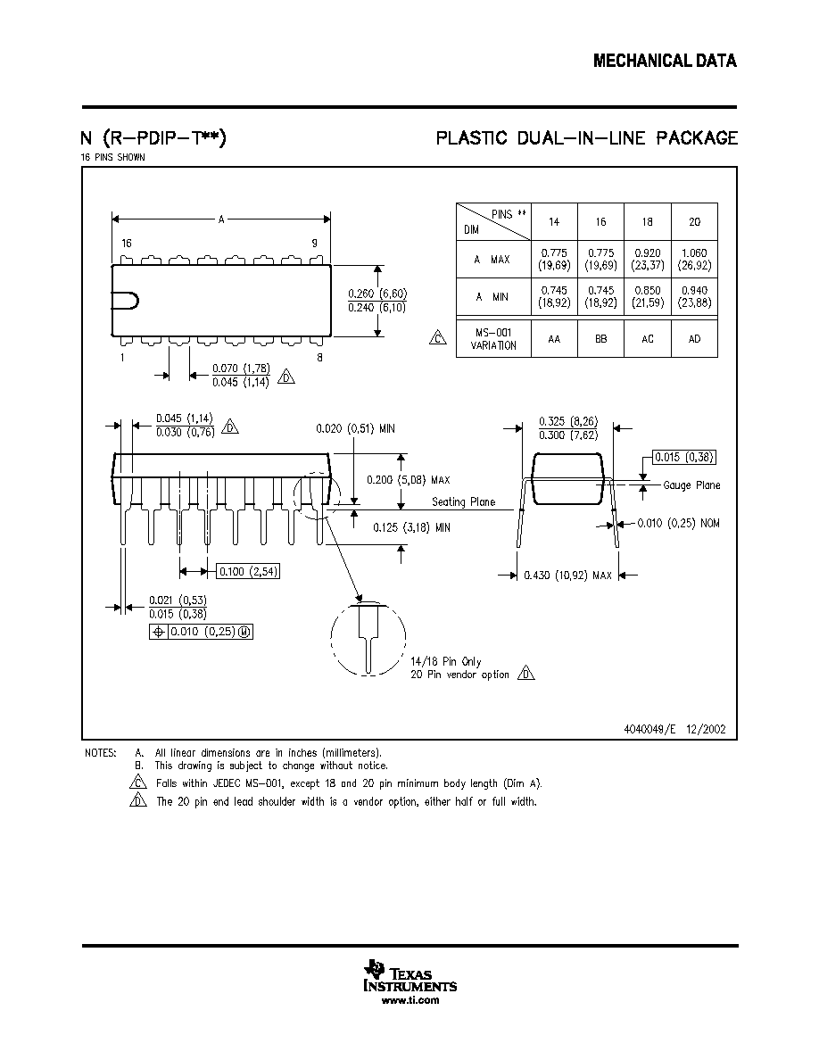
MECHANICAL DATA
MTSS001C ≠ JANUARY 1995 ≠ REVISED FEBRUARY 1999
POST OFFICE BOX 655303
∑
DALLAS, TEXAS 75265
PW (R-PDSO-G**)
PLASTIC SMALL-OUTLINE PACKAGE
14 PINS SHOWN
0,65
M
0,10
0,10
0,25
0,50
0,75
0,15 NOM
Gage Plane
28
9,80
9,60
24
7,90
7,70
20
16
6,60
6,40
4040064/F 01/97
0,30
6,60
6,20
8
0,19
4,30
4,50
7
0,15
14
A
1
1,20 MAX
14
5,10
4,90
8
3,10
2,90
A MAX
A MIN
DIM
PINS **
0,05
4,90
5,10
Seating Plane
0
∞
≠ 8
∞
NOTES: A. All linear dimensions are in millimeters.
B. This drawing is subject to change without notice.
C. Body dimensions do not include mold flash or protrusion not to exceed 0,15.
D. Falls within JEDEC MO-153

IMPORTANT NOTICE
Texas Instruments Incorporated and its subsidiaries (TI) reserve the right to make corrections, modifications,
enhancements, improvements, and other changes to its products and services at any time and to discontinue
any product or service without notice. Customers should obtain the latest relevant information before placing
orders and should verify that such information is current and complete. All products are sold subject to TI's terms
and conditions of sale supplied at the time of order acknowledgment.
TI warrants performance of its hardware products to the specifications applicable at the time of sale in
accordance with TI's standard warranty. Testing and other quality control techniques are used to the extent TI
deems necessary to support this warranty. Except where mandated by government requirements, testing of all
parameters of each product is not necessarily performed.
TI assumes no liability for applications assistance or customer product design. Customers are responsible for
their products and applications using TI components. To minimize the risks associated with customer products
and applications, customers should provide adequate design and operating safeguards.
TI does not warrant or represent that any license, either express or implied, is granted under any TI patent right,
copyright, mask work right, or other TI intellectual property right relating to any combination, machine, or process
in which TI products or services are used. Information published by TI regarding third-party products or services
does not constitute a license from TI to use such products or services or a warranty or endorsement thereof.
Use of such information may require a license from a third party under the patents or other intellectual property
of the third party, or a license from TI under the patents or other intellectual property of TI.
Reproduction of information in TI data books or data sheets is permissible only if reproduction is without
alteration and is accompanied by all associated warranties, conditions, limitations, and notices. Reproduction
of this information with alteration is an unfair and deceptive business practice. TI is not responsible or liable for
such altered documentation.
Resale of TI products or services with statements different from or beyond the parameters stated by TI for that
product or service voids all express and any implied warranties for the associated TI product or service and
is an unfair and deceptive business practice. TI is not responsible or liable for any such statements.
Following are URLs where you can obtain information on other Texas Instruments products and application
solutions:
Products
Applications
Amplifiers
amplifier.ti.com
Audio
www.ti.com/audio
Data Converters
dataconverter.ti.com
Automotive
www.ti.com/automotive
DSP
dsp.ti.com
Broadband
www.ti.com/broadband
Interface
interface.ti.com
Digital Control
www.ti.com/digitalcontrol
Logic
logic.ti.com
Military
www.ti.com/military
Power Mgmt
power.ti.com
Optical Networking
www.ti.com/opticalnetwork
Microcontrollers
microcontroller.ti.com
Security
www.ti.com/security
Telephony
www.ti.com/telephony
Video & Imaging
www.ti.com/video
Wireless
www.ti.com/wireless
Mailing Address:
Texas Instruments
Post Office Box 655303 Dallas, Texas 75265
Copyright
2005, Texas Instruments Incorporated