
UCC2946
UCC3946
SLUS247D ≠ APRIL 1997 ≠ REVISED JANUARY 2003
MICROPROCESSOR SUPERVISOR
WITH WATCHDOG TIMER
1
www.ti.com
FEATURES
D
Fully Programmable Reset Threshold
D
Fully Programmable Reset Period
D
Fully Programmable Watchdog Period
D
2% Accurate Reset Threshold
D
Input Voltage Down to 2 V
D
Input 18-
µ
A Maximum Input Current
D
Reset Valid Down to 1 V
DESCRIPTION
The UCCx946 is designed to provide accurate
microprocessor supervision, including reset and
watchdog functions. During power up, the device
asserts a reset signal RES with VDD as low as 1 V.
The reset signal remains asserted until the VDD
voltage rises and remains above the reset
threshold for the reset period. Both reset threshold
and reset period are programmable by the user.
The UCCx946 is also resistant to glitches on the
VDD line. Once RES has been deasserted, any
drops below the threshold voltage need to be of
certain time duration and voltage magnitude to
generate a reset signal. These values are shown
in Figure 1. An I/O line of the microprocessor may
be tied to the watchdog input (WDI) for watchdog
functions. If the I/O line is not toggled within a set
watchdog period, programmable by the user,
WDO is asserted. The watchdog function is
disabled during reset conditions.
The UCCx946 is available in 8-pin SOIC(D), 8-pin
PDIP (N) and 8-pin TSSOP(PW) packages to
optimize board space.
UDG≠02192
6
7
WDI
WP
8
VDD
3
5
POWER TO
CIRCUITRY
A3
A2
A1
A0
CLK
CLR
8≠BIT
COUNTER
400 nA
WDO
GND
EDGE DETECT
WATCHDOG
TIMING
100 mV
1.235 V
2
RTH
4
RP
400 nA
POWER ON RESET
RES
+
+
S
Q
Q
R
S
Q
Q
R
S
Q
Q
R
1
1.235 V
+
+
+
+
+
PRODUCTION DATA information is current as of publication date.
Products conform to specifications per the terms of Texas Instruments
standard warranty. Production processing does not necessarily include
testing of all parameters.
Copyright
2002, Texas Instruments Incorporated
UCC2946
UCC3946
SLUS247D ≠ APRIL 1997 ≠ REVISED JANUARY 2003
2
www.ti.com
ORDERING INFORMATION
T
PACKAGED DEVICES(3)
TA
(D)
(N)
(PW)
≠40
∞
C to 95
∞
C
UCC2946D
UCC2946N
UCC2946PW
0
∞
C to 70
∞
C
UCC3946D
UCC3946N
UCC3946PW
(1) The D and PW packages are also available taped and reeled. Add an R suffix to the device type (i.e., UCC2946DR) for quantities of 3,000
devices per reel.
These devices have limited built-in ESD protection. The leads should be shorted together or the device placed in conductive foam
during storage or handling to prevent electrostatic damage to the MOS gates.
ABSOLUTE MAXIMUM RATINGS
over operating free-air temperature range unless otherwise noted(1)
UCC2946
UCC3946
UNIT
Input voltage range, VIN
10
V
Junction temperature range, TJ
≠55 to 150
Storage temperature, Tstg
≠65 to 150
∞
C
Lead temperature 1,6 mm (1/16 inch) from case for 10 seconds
300
C
(1) Stresses beyond those listed under "absolute maximum ratings" may cause permanent damage to the device. These are stress ratings only,
and functional operation of the device at these or any other conditions beyond those indicated under "recommended operating conditions" is
not implied. Exposure to absolute-maximum-rated conditions for extended periods may affect device reliability. Voltages are with respect to
GND. Currents are positive into, and negative out of the specified terminal.
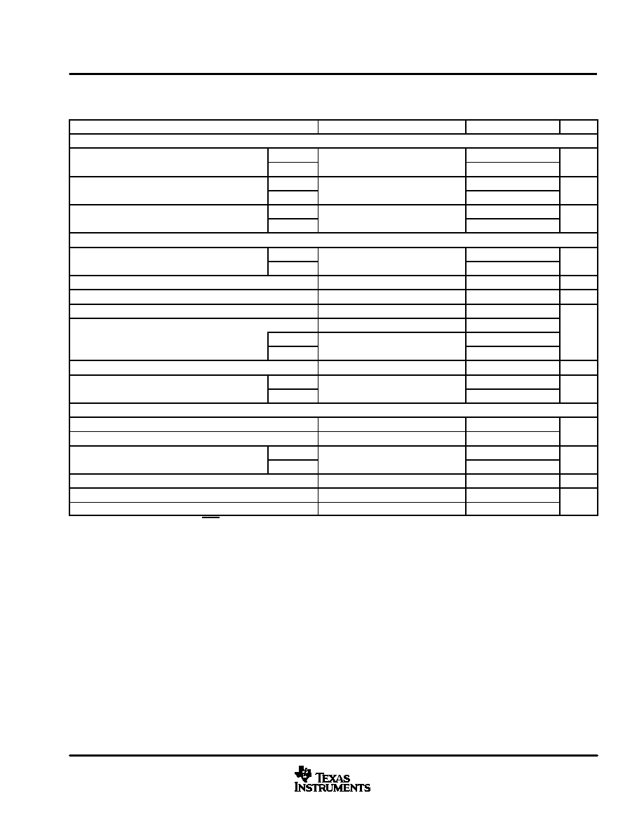
1
2
3
4
8
7
6
5
GND
RTH
RES
RP
VDD
WDI
WP
WDO
D PACKAGE
(TOP VIEW)
TERMINAL FUNCTIONS
TERMINAL
I/O
DESCRIPTION
NAME
NO.
I/O
DESCRIPTION
GND
1
≠
Ground reference for the device
RES
3
O
This pin is high only if the voltage on the RTH has risen above 1.235 V. Once RTH rises above the threshold, this
pin remains low for the reset period. This pin asserts low and remains low if the RTH voltage dips below 1.235 V for
an amount of time determined by Figure 1.
RTH
2
I
This input compares its voltage to an internal 1.25-V reference. By using external resistors, a user can program any
desired reset threshold.
RP
4
I
This pin allows the user to program the reset period by adjusting an external capacitor.
VDD
8
I
Supply voltage for the device.
WDI
7
I
This pin is the input to the watchdog timer. If this pin is not toggled or strobed within the watchdog period, WDO is
asserted.
WDO
5
O
This pin is the watchdog output. This pin is asserted low if the WDI pin is not strobed or toggled within the watchdog
period.
WP
6
I
This pin allows the user to program the watchdog period by adjusting an external capacitor.
UCC2946
UCC3946
SLUS247D ≠ APRIL 1997 ≠ REVISED JANUARY 2003
3
www.ti.com
ELECTRICAL CHARACTERISTICS
TA = 0
∞
C to 70
∞
C and 2.0 V
VDD
5.5 V for the UCC3946, TA = ≠40
∞
C to 95
∞
C and 2.1 V
VDD
5.5 V for the UCC2946, (unless
otherwise noted)
PARAMETER
TEST CONDITIONS
MIN
TYP
MAX
UNIT
REFERENCE
V
Operating oltage
UCC2946
2.1
5.5
V
VDD
Operating voltage
UCC3946
2.0
5.5
V
I
Supply current
UCC2946
12
18
A
IDD
Supply current
UCC3946
10
18
µ
A
V
Minimum operating voltage(1)
UCC2946
1.1
V
VDD(min)
Minimum operating voltage(1)
UCC3946
1.0
V
RESET SECTION
Reset threshold voltage
UCC2946
V
rising
1.170
1.235
1.260
V
Reset threshold voltage
UCC3946
VDD rising
1.190
1.235
1.260
V
Threshold hysteresis
15
mV
ILEAK
Input leakage current
5
nA
VOH
High-level output voltage
ISOURCE = 2 mA
VDD≠0.3
ISINK = 2 mA
0.1
V
VOL
Low level output voltage
UCC2946
I
20 A
VDD
1 V
0.4
V
VOL
Low-level output voltage
UCC3946
ISINK = 20
µ
A,
VDD = 1 V
0.2
VDD-to-output delay time
VDD = ≠1 mV/
µ
s
120
µ
s
Reset period
UCC2946
C
64 nF
140
200
320
ms
Reset period
UCC3946
CRP = 64 nF
160
200
260
ms
WATCHDOG SECTION
VIH
High-level input voltage, WDI
0.7
◊
VDD
V
VIL
Low-level input voltage, WDI
0.3
◊
VDD
V
Watchdog period
UCC2946
C
64 nF
0.96
1.60
2.56
s
Watchdog period
UCC3946
CRP = 64 nF
1.12
1.60
2.08
s
Watchdog pulse width
50
ns
VOH
High-level output voltage
ISOURCE = 2 mA
VDD≠0.3
V
VOL
Low-level output voltage
ISINK = 2 mA
0.1
V
(1) Minimum supply voltage where RES is considered valid.

UCC2946
UCC3946
SLUS247D ≠ APRIL 1997 ≠ REVISED JANUARY 2003
4
www.ti.com
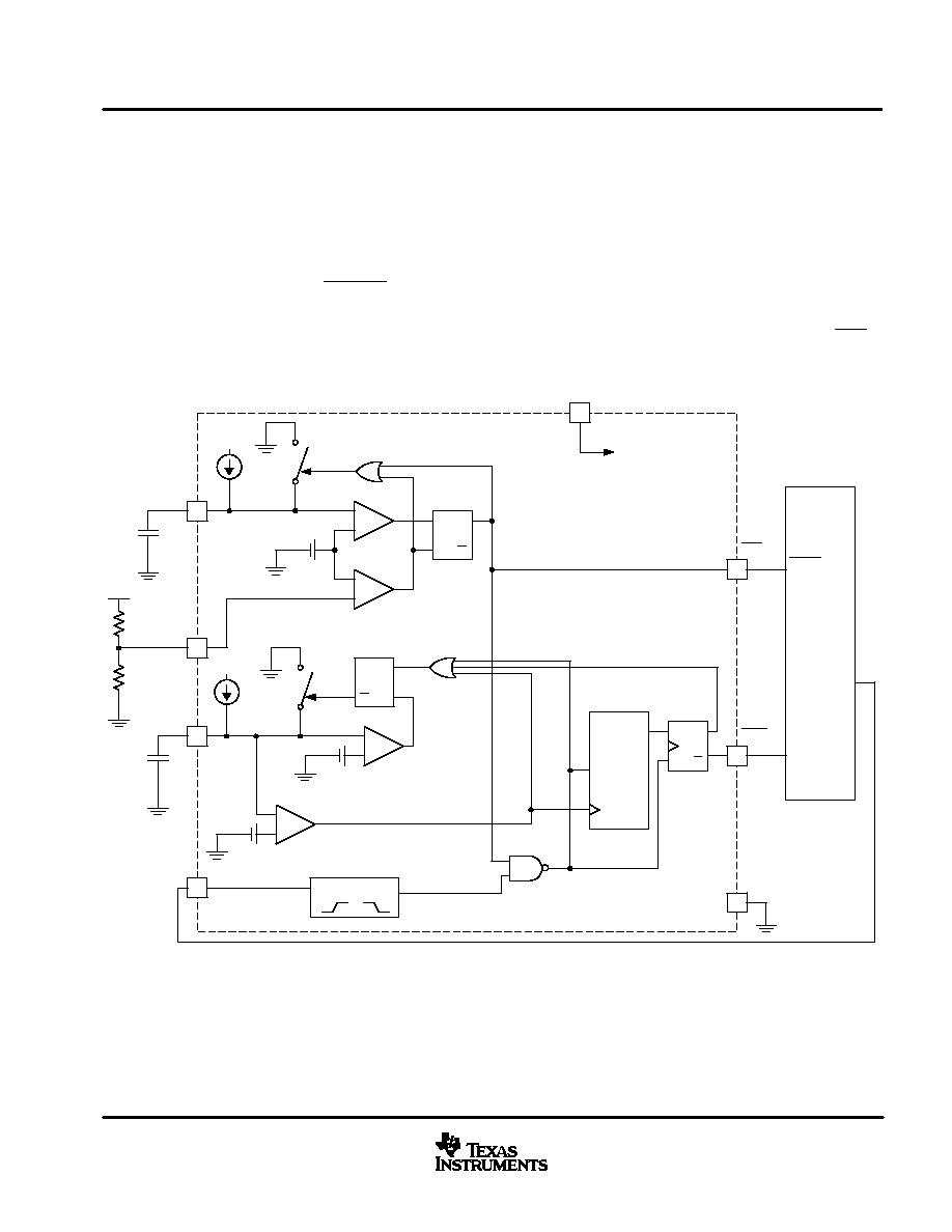
APPLICATION INFORMATION
The UCCx946 supervisory circuit provides accurate reset and watchdog functions for a variety of
microprocessor applications. The reset circuit prevents the microprocessor from executing code during
undervoltage conditions, typically during power-up and power-down. In order to prevent erratic operation in the
presence of noise, voltage glitches where voltage amplitude and time duration are less than the values specified
in Figure 1 are ignored.
100
40
0
110
120
130
140
150
160
170
180
20
100
60
80
120
180
140
160
200
Figure 1.
OVERDRIVE VOLTAGE WITH RESPECT TO
RESET THRESHOLD
vs
DELAY TO OUTPUT LOW ON R
ESB
V
TH
≠
Overdrive V
oltage
≠
mV
TDELAY ≠ Delay Time ≠
µ
s
RT Senses Glitch,
RES Goes Low for Reset Period
Glitches
Ignored,
RESB
Remains
High
The watchdog circuit monitors the microprocessor's activity, if the microprocessor does not toggle WDI during
the programmable watchdog period WDO goes low, alerting the microprocessor's interrupt of a fault. The WDO
pin is typically connected to the non-maskable input of the microprocessor so that an error recovery routine can
be executed.
UCC2946
UCC3946
SLUS247D ≠ APRIL 1997 ≠ REVISED JANUARY 2003
5
www.ti.com
APPLICATION INFORMATION
PROGRAMMING THE RESET VOLTAGE AND RESET PERIOD
The UCCx946 allows the reset trip voltage to be programmed with two external resistors. In most applications
VDD is monitored by the reset circuit, however, the design allows voltages other than VDD to be monitored.
Referring to Figure 2, the voltage below which reset is asserted is determined by:
V
RESET
+
1.235
R1
)
R2
R2
In order to keep quiescent currents low, resistor values in the megaohm range can be used for R1 and R2. A
manual reset can be easily implemented by connecting a momentary push switch in parallel with R2. RES is
ensured to be low with VDD voltages as low as 1 V.
UDG≠98002
6
7
WDI
WP
8
VDD
3
5
POWER TO
CIRCUITRY
WDO
GND
EDGE DETECT
WATCHDOG
TIMING
100 mV
2
RTH
4
RP
400 nA
POWER
ON RESET
VDD
RESET
NMI
I/O
uP
RES
+
≠
+
≠
+
≠
+
≠
+
S
Q
Q
R
1.235 V
S
Q
Q
R
R2
R1
400 nA
+
+
1.235 V
A3
A2
A1
A0
CLK
CLR
8≠BIT
COUNTER
S
Q
Q
R
1
CRP
CWP
Figure 2. Typical Application Diagram
(1)
UCC2946
UCC3946
SLUS247D ≠ APRIL 1997 ≠ REVISED JANUARY 2003
6
www.ti.com
APPLICATION INFORMATION
Once VDD rises above the programmed threshold, RES remains low for the reset period defined by:
T
RP
+
3.125
C
RP
where T
RP
is time in milliseconds and C
RP
is capacitance in nanofarads. C
RP
is charged with a precision current
source of 400 nA, a high-quality, low-leakage capacitor (such as an NPO ceramic) should be used to maintain
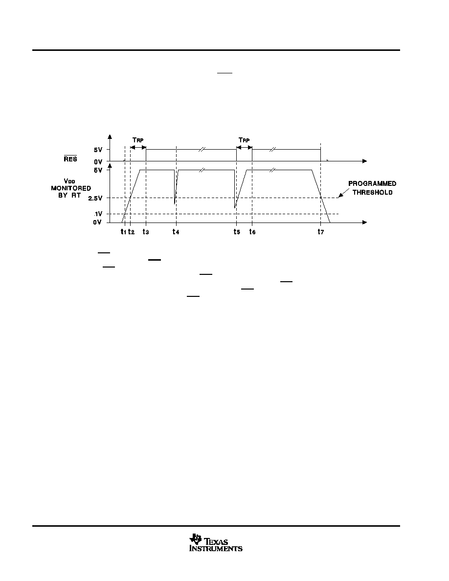
timing tolerances. Figure 3 illustrates the voltage levels and timings associated with the reset circuit.
UDG≠97067
t1: VDD > 1 V, RES is ensured low.
t2: VDD > programmed threshold, RES remains low for TRP.
t3: TRP expires, RES pulls high.
t4: Voltage glitch occurs, but is filtered at the RTH pin, RES remains high.
t5: Voltage glitch occurs whose magnitude and duration is greater than the RTH filter, RES is asserted for TRP.
t6: On completion of the TRP pulse the RTH voltage has returned and RES is pulled high.
t7: VDD dips below threshold (minus hysteresis), RES is asserted.
Figure 3. Reset Circuit Timings
(2)

UCC2946
UCC3946
SLUS247D ≠ APRIL 1997 ≠ REVISED JANUARY 2003
7
www.ti.com
APPLICATION INFORMATION
PROGRAMMING THE WATCHDOG PERIOD
The watchdog period is programmed with C
WP
as follows:
T
WP
+
25
C
WP
where T
WP
is in milliseconds and C
WP
is in nanofarads. A high-quality, low-leakage capacitor should be used
for C
WP
. The watchdog input WDI must be toggled with a high-to-low or low-to-high transition within the
watchdog period to prevent WDO from assuming a logic level low. WDO maintains the low logic level until WDI
is toggled or RES is asserted. If at any time RES is asserted, WDO assumes a high logic state and the watchdog
period be reinitiated. Figure 4 illustrates the timings associated with the watchdog circuit.
0V
VDD
t1
0V
VDD
VDD
0V
t2
t3
t4
t5
t6
t7
t8
t9
t10 t11
t12
t13
t14
RESET
WDI
WDO
TRP
TWP
UDG≠98007
t1: Microprocessor is reset.
t2: WDI is toggled some time after reset, but before TWP expires.
t3: WDI is toggled before TWP expires.
t4: WDI is toggled before TWP expires.
t5: WDI is not toggled before TWP expires and WDO asserts low, triggering the microprocessor to enter an error recovery routine.
t6: The
microprocessor's error recovery routine is executed and WDI is toggled, reinitiating the watchdog timer.
t7: WDI is toggled before TWP expires.
t8: WDI is toggled before TWP expires.
t9: RES is momentarily triggered, RES is asserted low for TRP.
t10: Microprocessor is reset, RES pulls high.
t11: WDI is toggled some time after reset, but before TWP expires.
t12: WDI is toggled before TWP expires.
t13: WDI is toggled before TWP expires.
t14: VDD dips below the reset threshold, RES is asserted.
Figure 4. Watchdog Circuit Timings
(3)

UCC2946
UCC3946
SLUS247D ≠ APRIL 1997 ≠ REVISED JANUARY 2003
8
www.ti.com
APPLICATION INFORMATION
CONNECTING WDO TO RES
In order to provide design flexibility, the reset and watchdog circuits in the UCCx946 have separate outputs.
Each output independently drives high or low, depending on circuit conditions explained previously.
In some applications, it may be desirable for either the RES or WDO to reset the microprocessor. This can be
done by connecting WDO to RES. If the pins try to drive to different output levels, the low output level dominates.
Additional current flows from VDD to GND during these states. If the application cannot support additional
current (during fault conditions), RES and WDO can be connected to the inputs of an OR gate whose output
is connected to the microprocessor's reset pin.
LAYOUT CONSIDERATIONS
A 0.1-
µ
F capacitor connected from VDD to GND is recommended to decouple the UCCx946 from switching
transients on the VDD supply rail.
Since RP and WP are precision current sources, capacitors C
RP
and C
WP
should be connected to these pins
with minimal trace length to reduce board capacitance. Care should be taken to route any traces with high
voltage potential or high speed digital signals away from these capacitors.
Resistors R1 and R2 generally have a high ohmic value, traces associated with these parts should be kept short
in order to prevent any transient producing signals from coupling into the high impedance RTH pin.
TYPICAL CHARACTERISTICS
Figure 5.
THRESHOLD RESISTANCE
vs
AMBIENT TEMPERATURE
V
RTH
≠
Threshold Resistance
≠
V
TA ≠ Ambient Temperature ≠
∞
C
≠55
1.22
1.20
≠35
≠15
5
25
45
65
85
105
125
1.21
1.25
1.23
1.24
1.26
VDD = 5 V
2
10.0
9.0
3
4
5
6
9.5
11.5
10.5
11.0
12.0
Figure 6.
VDD ≠ Input Voltage ≠ V
INPUT CURRENT
vs
INPUT VOLTAGE
I DD
≠
Input Current
≠
µ
A

IMPORTANT NOTICE
Texas Instruments Incorporated and its subsidiaries (TI) reserve the right to make corrections, modifications,
enhancements, improvements, and other changes to its products and services at any time and to discontinue
any product or service without notice. Customers should obtain the latest relevant information before placing
orders and should verify that such information is current and complete. All products are sold subject to TI's terms
and conditions of sale supplied at the time of order acknowledgment.
TI warrants performance of its hardware products to the specifications applicable at the time of sale in
accordance with TI's standard warranty. Testing and other quality control techniques are used to the extent TI
deems necessary to support this warranty. Except where mandated by government requirements, testing of all
parameters of each product is not necessarily performed.
TI assumes no liability for applications assistance or customer product design. Customers are responsible for
their products and applications using TI components. To minimize the risks associated with customer products
and applications, customers should provide adequate design and operating safeguards.
TI does not warrant or represent that any license, either express or implied, is granted under any TI patent right,
copyright, mask work right, or other TI intellectual property right relating to any combination, machine, or process
in which TI products or services are used. Information published by TI regarding third≠party products or services
does not constitute a license from TI to use such products or services or a warranty or endorsement thereof.
Use of such information may require a license from a third party under the patents or other intellectual property
of the third party, or a license from TI under the patents or other intellectual property of TI.
Reproduction of information in TI data books or data sheets is permissible only if reproduction is without
alteration and is accompanied by all associated warranties, conditions, limitations, and notices. Reproduction
of this information with alteration is an unfair and deceptive business practice. TI is not responsible or liable for
such altered documentation.
Resale of TI products or services with statements different from or beyond the parameters stated by TI for that
product or service voids all express and any implied warranties for the associated TI product or service and
is an unfair and deceptive business practice. TI is not responsible or liable for any such statements.
Mailing Address:
Texas Instruments
Post Office Box 655303
Dallas, Texas 75265
Copyright
2003, Texas Instruments Incorporated