 | –≠–ª–µ–∫—Ç—Ä–æ–Ω–Ω—ã–π –∫–æ–º–ø–æ–Ω–µ–Ω—Ç: UCC3952-4 | –°–∫–∞—á–∞—Ç—å:  PDF PDF  ZIP ZIP |
UCC3952-1/-2/-3/-4
DESCRIPTION
The UCC3952 is a monolithic BiCMOS lithium-ion battery protection circuit
that is designed to enhance the useful operating life of one cell recharge-
able battery pack. Cell protection features consist of internally trimmed
charge and discharge voltage limits, discharge current limit with a delayed
shutdown and an ultra low current sleep mode state when the cell is dis-
charged. Additional features include an on chip MOSFET for reduced exter-
nal component count and a charge pump for reduced power losses while
charging or discharging a low cell voltage battery pack. This protection cir-
cuit requires one external capacitor and is able to operate and safely shut-
down in the presence of a short circuit condition.
Enhanced Single Cell Lithium-Ion Battery Protection IC
FEATURES
∑
Protects sensitive Lithium Ion cells
from over-charging and
over-discharging
∑
Dedicated for one cell applications
∑
Integrated low impedance MOSFET
switch and sense resistor
∑
Precision trimmed overcharge and
overdischarge voltage limits
∑
Extremely low power drain
∑
3A current capacity
∑
Overcurrent and Short Circuit
Protection
∑
Reverse Charger Protection
∑
Thermal Protection
SLUS400A - FEBRUARY 2000
1
3
2
4
5
7
6
8
16
14
15
13
12
10
11
9
0.1
µ
F
3k
TCLK
N/C
BNEG
BNEG
BNEG
BNEG
BNEG
BNEG
PACK≠
PACK≠
PACK≠
PACK≠
PACK≠
N/C
CBPS
PACK+
LOAD
CHARGER
+
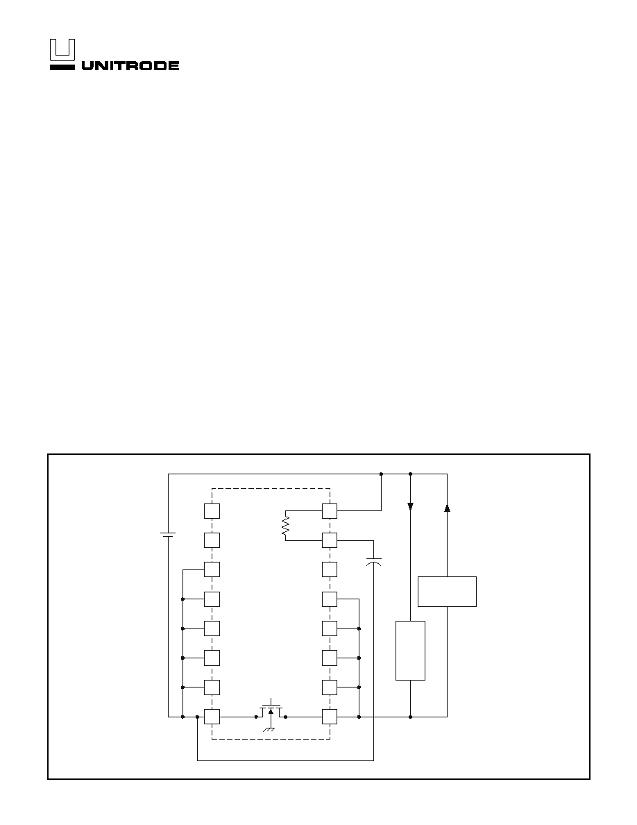
APPLICATION DIAGRAM
UDG-98205
2
UCC3952-1/-2/-3/-4
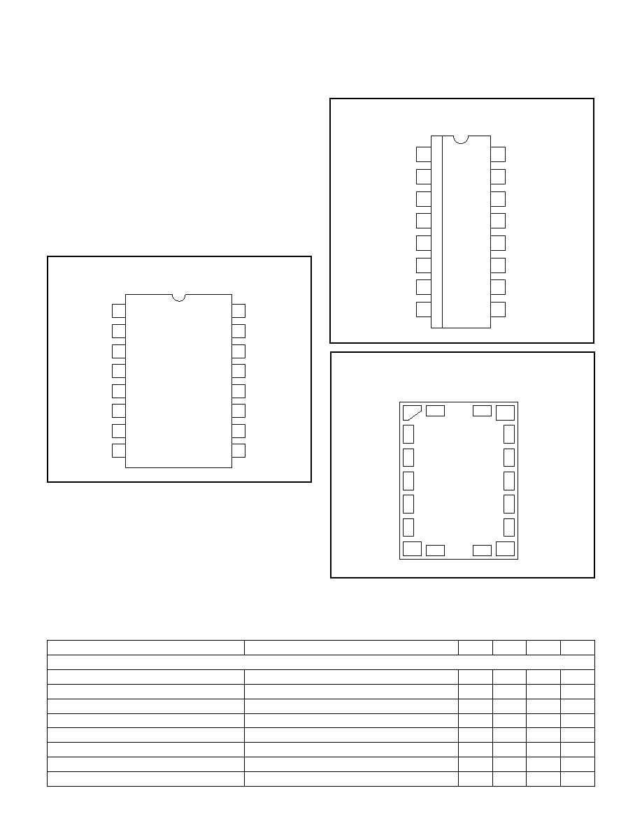
SOIC-16 (TOP VIEW)
DP Package
ABSOLUTE MAXIMUM RATINGS
Supply Voltage (PACK+ to BNEG) . . . . . . . . . . . . . . . . . . . . 7V
Maximum Forward Voltage (PACK+ to PACK≠) . . . . . . . . . 16V
Maximum Reverse Voltage
(where PACK+ to BNEG = 5V) . . . . . . . . . . . . . . . . . . . . . ≠8V
Maximum Cell Continuous Charge Current . . . . . . . . . . . . . . 3A
Junction Temperature . . . . . . . . . . . . . . . . . . . . ≠55∞C to 150∞C
Storage Temperature Range . . . . . . . . . . . . . . ≠40∞C to 125∞C
Currents are positive into, negative out of the specified termi-
nal. Consult Packaging Section of Databook for thermal limita-
tions and considerations of packages. All voltages are
referenced to GND.
1
2
3
4
5
6
7
8
16
15
14
13
12
11
10
9
N/C
TCLK
BNEG
BNEG
BNEG
N/C
SUB
SUB
SUB
SUB
N/C
PACK+
CBPS
PACK≠
PACK≠
PACK≠
CONNECTION DIAGRAMS
PACK+
N/C
BNEG
BNEG
BNEG
BNEG
BNEG
TCLK
BNEG
8
7
6
5
4
3
2
1
9
10
11
12
13
14
15
16
CBPS
N/C
PACK≠
PACK≠
PACK≠
PACK≠
PACK≠
TSSOP-16 (TOP VIEW)
PW Package
ELECTRICAL CHARACTERISTICS:
Temperature Range: ≠20∞C < T
A
< 70∞C, Unless otherwise stated. All voltages are
with respect to BNEG. T
A
= T
J
PARAMETER
TEST CONDITIONS
MIN
TYP
MAX
UNITS
State Transition Threshold Section
NORM to OV (V
OV
)
UCC3952-1
4.15
4.20
4.25
V
OV to NORM (V
OVR)
UCC3952-1
3.85
3.90
3.95
V
NORM to OV (V
OV
)
UCC3952-2
4.20
4.25
4.30
V
OV to NORM (V
OVR)
UCC3952-2
3.90
3.95
4.00
V
NORM to OV (V
OV
)
UCC3952-3
4.25
4.30
4.35
V
OV to NORM (V
OVR)
UCC3952-3
3.95
4.00
4.05
V
NORM to OV (V
OV
)
UCC3952-4
4.30
4.35
4.40
V
OV to NORM (V
OVR)
UCC3952-4
4.00
4.05
4.10
V
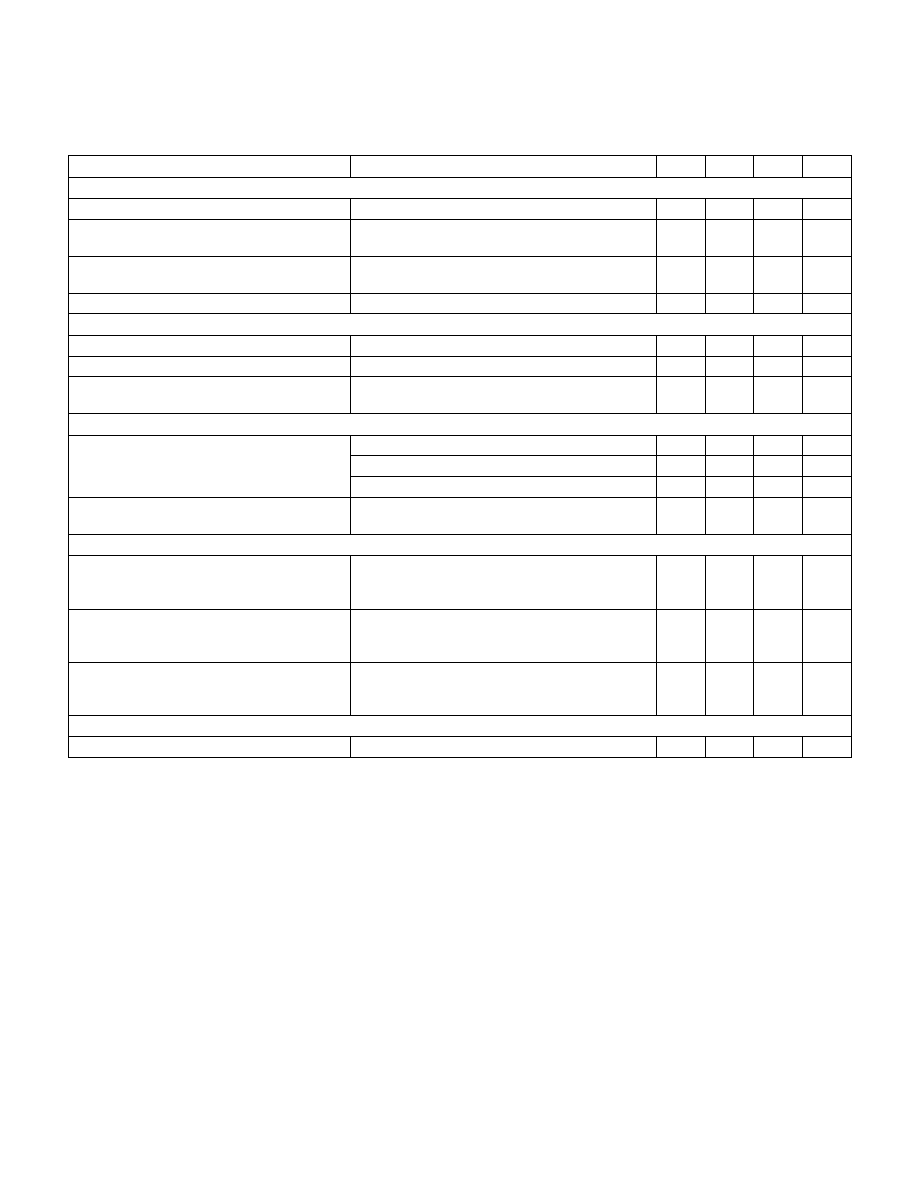
N/C
18
17
7
10
8
9
1
N/C
16
BNEG
CBPS
N/C
PACK≠
TCLK
PACK+
N/C
BNEG BNEG
PACK≠
15
14
2
3
4
5
BNEG
BNEG
BNEG
6
13
12
PACK≠
PACK≠ 11
PACK≠
Consult factory for GSH package availability.
BCC-18 (TOP VIEW)
GSH Package
3
UCC3952-1/-2/-3/-4
ELECTRICAL CHARACTERISTICS:
Temperature Range: ≠20∞C < T
A
< 70∞C, Unless otherwise stated. All voltages are
with respect to BNEG. T
A
= T
J
PARAMETER
TEST CONDITIONS
MIN
TYP
MAX
UNITS
State Transition Threshold Section (cont.)
OV Delay Time (T
OV
)
1
2
sec
NORM to UV (V
UV
)
UCC3952-1, UCC3952-2, UCC3952-3,
UCC3952-4
2.25
2.35
2.45
V
UV to NORM (V
UVR)
UCC3952-1, UCC3952-2, UCC3952-3,
UCC3952-4
2.55
2.65
2.75
V
Overdischarge Delay Time (T
OD
)
10
25
40
ms
Short Circuit Protection Section
ITHLD
Discharge current limit, PACK+ = 3.7V
3.0
4.5
A
TDLY
Discharge current delay, PACK+ = 3.7V, I = 6A
1
2.5
ms
R
RESET
Discharge current reset resistance,
PACK+ = 4.0
7.5
M
Bias Section
IDD
Normal operating current. V
UV
< V
PACK
< V
OV
5
8
µ
A
Operating current in overvoltage V
OV
< V
PACK
11
24
µ
A
Shutdown operating current V
PACK
< V
UV
2.5
µ
A
V
MIN
Minimum cell voltage when all circuits are
guaranteed to be fully functional
1.7
V
FET Switch Section
V
PACK
≠
PACK+ > V
OV
, I(SWITCH) = 1mA to 2A
Battery overcharged state switch permits
discharge current only.
100
400
mV
V
PACK
≠
PACK+ = 2.5V, I(SWITCH) = ≠1mA to ≠2A
Battery overdischarged state switch permits
charge current only.
≠600
≠100
mV
R
ON
In Normal Mode (when not in OV or UV). This
value includes package and bondwire resistance.
PACK+ = 2.5V
50
75
m
Thermal Shutdown Section
TS
Thermal shutdown temperature. (Note 1)
135
∞
C
Note 1. This parameter is guaranteed by design. Not 100% tested in production.
BNEG: Connect the negative terminal of the battery to
this pin.
PACK+: Connect to the positive terminal of the battery.
This pin is available to the user.
CBPS: This power supply bypass pin is connected to
PACK+ through an internal 10K resistor.
An external
0.1 F capacitor must be connected between this pin and
BNEG.
PACK≠: The negative terminal of the battery pack (nega-
tive terminal available to the user).
The internal FET
switch connects this terminal to the BNEG terminal to
give the battery pack user appropriate access to the bat-
tery. In an over-charged state, only discharge current is
permitted. In an over-discharged state, only charge cur-
rent is permitted.
SUB: (DP Package Only) Do not connect. These pins
must be electrically isolated from all other pins. These
pins may be soldered to isolated coppper pads for
heatsinking. However, most applications do not require
heatsinking.
TCLK: Production Test Mode pin. This pin is used to
provide a high frequency clock to the IC during produc-
tion testing. In an application this pin may be left uncon-
nected, or tied to BNEG.
PIN DESCRIPTIONS
4
UCC3952-1/-2/-3/-4
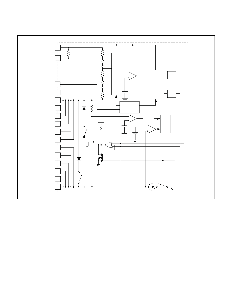
12
10
11
9
7
8
2
13
14
5
3
4
1
16
15
6
V
PUMP
TDLS
1mS
SETD
RST
SYSTEM
CLOCK
GENERATOR
SEL
4-1
MUX
V
UV
V
OV
V
UVR
V
OVR
THRESHOLD
COMPARATOR
THERMAL
SHUTDOWN
50mV
50mV
2M
10K
1.5V
PACK+
CBPS
TCLK
BNEG
BNEG
BNEG
BNEG
BNEG
BNEG
PACK≠
PACK≠
PACK≠
PACK≠
PACK≠
PACK≠
N/C
T
DEL
1SEC
T
DEL
10mS
STATE
MACHINE
LOGIC
OV
UV
CLK
APPLICATION INFORMATION
Figure 1. Detailed block diagram.
UDG-98209
Fig. 1 shows a detailed block diagram of the UCC3952.
Battery Voltage Monitoring
The battery cell voltage is sampled every 8ms by con-
necting a resistor divider across it and comparing the re-
sulting voltage to a precision internal reference voltage.
Under normal conditions (cell voltage is below Over Volt-
age threshold and above Under Voltage threshold), the
UCC3952 consumes less than 10 A of current and the
internal MOSFET is fully turned on with the aid of a
charge pump.
When the cell voltage falls below the Under Voltage
threshold for two consecutive samples, the IC discon-
nects the load from the battery pack and enters a super
low power mode. The pack will remain in this state until it
detects the application of a charger, at which point
charging is enabled. The requirement of two consecutive
readings below the UV threshold filters out momentary
drops in cell voltage due to load transients, preventing
nuisance trips.
If the cell voltage exceeds the Over Voltage threshold for
1sec, charging is disabled, however discharge current is
still allowed. This feature of the IC is explained further in
the section on Controlled Charge/Discharge Mode.
APPLICATION INFORMATION
PW package shown

5
UCC3952-1/-2/-3/-4
Over Current Monitoring and Protection
Discharge current is continuously monitored via an inter-
nal sense resistor. In the event of excessive current, an
Over Current condition is declared if the high current
(over 3A) persists for over 1ms. This delay allows for
charging of the system bypass capacitors without trip-
ping the overcurrent. A 0.1 F capacitor on the CBPS pin
provides momentary holdup for the IC to assure proper
operation in the event that a hard short suddenly pulls
the cell voltage below the minimum operating voltage.
Once an Over Current condition has been declared, the
internal MOSFET turns off. The only way to return the
pack to normal operation is to remove the load by un-
plugging the pack from the system. The overcurrent is re-
set when an internal pull down brings PACK(≠) to within
50mV of BNEG. At this point, the pack returns to its nor-
mal state of operation.
Controlled Charge/Discharge Mode
When the chip senses an over-voltage condition, it pre-
vents any additional charging, but allows discharge. This
is accomplished by activating a linear control loop which
controls the gate of the MOSFET based on the differen-
tial voltage across its drain to source terminals. The lin-
ear loop attempts to regulate the differential voltage
across the MOSFET to 100mV. When a light load is ap-
plied to the part, the loop adjusts the impedance of the
MOSFET to maintain 100mV across it. As the load in-
creases, the impedance of the MOSFET is decreased to
maintain the 100mV control. At heavy loads (still below
"over-current" limit level), the loop will not maintain regu-
lation and will drive the gate of the MOSFET to the bat-
tery voltage (not the charge-pump output voltage). The
MOSFET R
DS(on)
in the over-voltage state will be higher
than R
DS(on)
during normal operation. The voltage drop
(and associated power loss) across the internal MOSFET
in this mode of operation is still significantly lower than
the
typical
solution
of
two
external
back-to-back
MOSFETs, where the body diode is conducting.
When the chip senses an under-voltage condition, it dis-
connects the load from the battery pack and shuts itself
down to minimize current drain from the battery. Several
circuits remain powered and will detect placement of the
battery pack into a charger. Once the charger presence
is detected, the linear loop is activated and the chip al-
lows charging current into the battery. This linear control
mode of operation is in effect until the battery voltage
reaches a level of V
UVR
, at which time normal operation
is resumed.
APPLICATION INFORMATION (cont.)
UNITRODE CORPORATION
7 CONTINENTAL BLVD. ∑ MERRIMACK, NH 03054
TEL. (603) 424-2410 ∑ FAX (603) 424-3460