UCC3952A-1, UCC3952A-2, UCC3952A-3, UCC3952A-4
SINGLE CELL LITHIUM ION BATTERY PROTECTION IC
SLUS463C ≠ AUGUST 2000 ≠ REVISED MARCH 2001
1
POST OFFICE BOX 655303
∑
DALLAS, TEXAS 75265
POST OFFICE BOX 1443
∑
HOUSTON, TEXAS 77251≠1443
D
Protects Sensitive Lithium-Ion Cells From
Overcharging and Over-Discharging
D
Dedicated for One-Cell Applications
D
Integrated Low-Impedance MOSFET Switch
and Sense Resistor
D
Precision Trimmed Overcharge and
Overdischarge Voltage Limits
D
Extremely Low Power Drain
D
3.5-A Current Capacity
D
Overcurrent and Short-Circuit Protection
D
Reverse Charger Protection
D
Thermal Protection
description
The UCC3952A is a monolithic BiCMOS lithium≠ion battery protection circuit designed to enhance the useful
operating life of a one-cell rechargeable battery pack. Cell protection features include internally trimmed charge
and discharge voltage limits, discharge current limit with a delayed shutdown, and an ultra-low-current sleep
mode state when the cell is discharged. Additional features include an on-chip MOSFET for reduced external
component count and a charge pump for reduced power losses while charging or discharging a low-cell-voltage
battery pack. This protection circuit requires one external capacitor and can operate and safely shut down in
a short circuit condition.
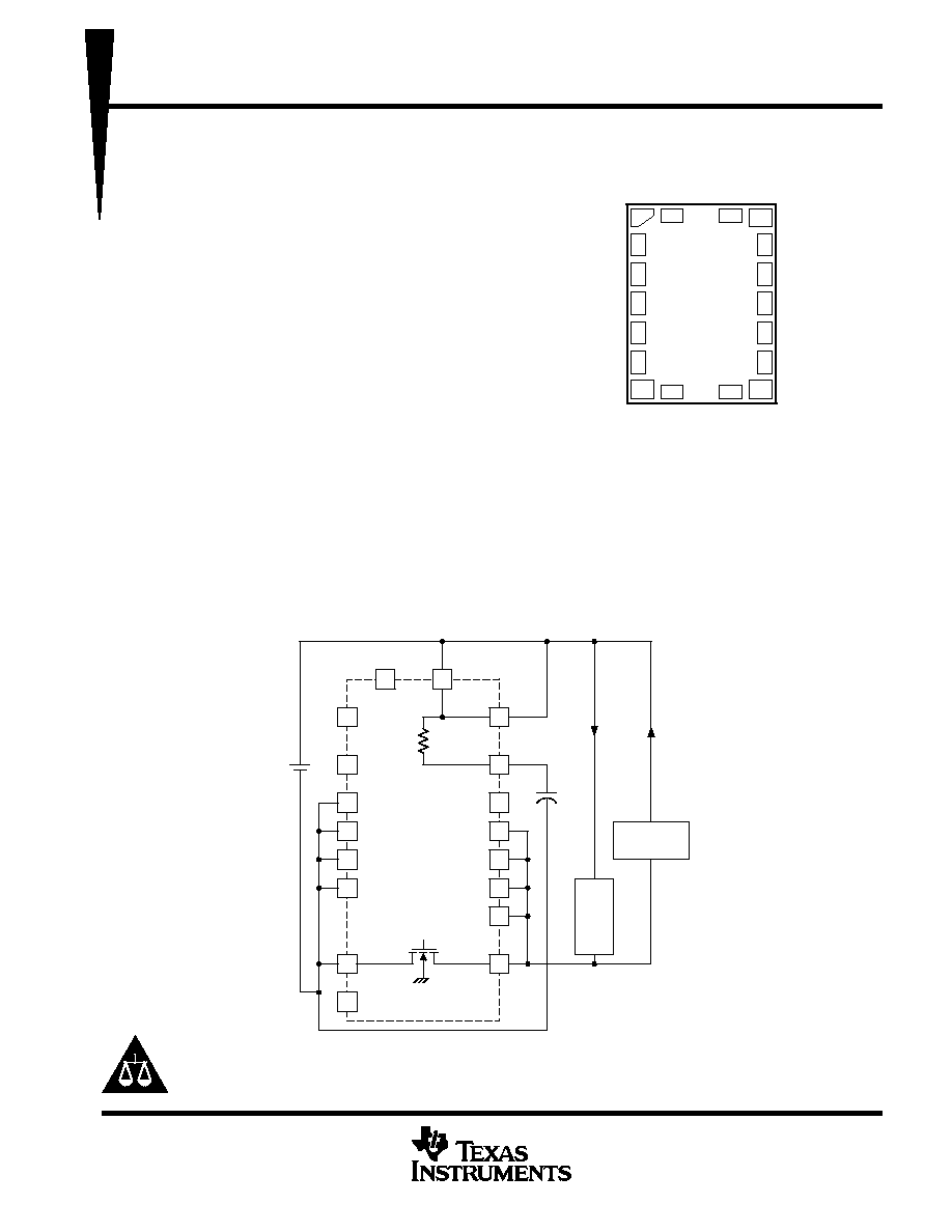
application diagram
UDG≠98205
18
3
2
4
5
7
6
8
16
14
15
13
12
10
11
9
0.1
µ
F
TCLK
NC
BNEG
BNEG
BNEG
NC
PACK≠
PACK≠
PACK≠
PACK≠
PACK≠
NC
CBPS
PACK+
LOAD
CHARGER
+
1
NC
17
PACK+
BNEG
BNEG
3 k
Copyright
2001, Texas Instruments Incorporated
Please be aware that an important notice concerning availability, standard warranty, and use in critical applications of
Texas Instruments semiconductor products and disclaimers thereto appears at the end of this data sheet.
18
17
7
10
8
9
1
NC
16
BNEG
CBPS
NC
PACK≠
15
14
2
3
4
5
BNEG
BNEG
BNEG
6
13
12
11
PACK≠
PACK≠
BNEG
PACK≠
PACK+
NC
GSH PACKAGE
(TOP VIEW)
TCLK
P
A
CK+
NC
P
ACK≠
PRODUCTION DATA information is current as of publication date.
Products conform to specifications per the terms of Texas Instruments
standard warranty. Production processing does not necessarily include
testing of all parameters.
UCC3952A-1, UCC3952A-2, UCC3952A-3, UCC3952A-4
SINGLE CELL LITHIUM ION BATTERY PROTECTION IC
SLUS463C ≠ AUGUST 2000 ≠ REVISED MARCH 2001
2
POST OFFICE BOX 655303
∑
DALLAS, TEXAS 75265
POST OFFICE BOX 1443
∑
HOUSTON, TEXAS 77251≠1443
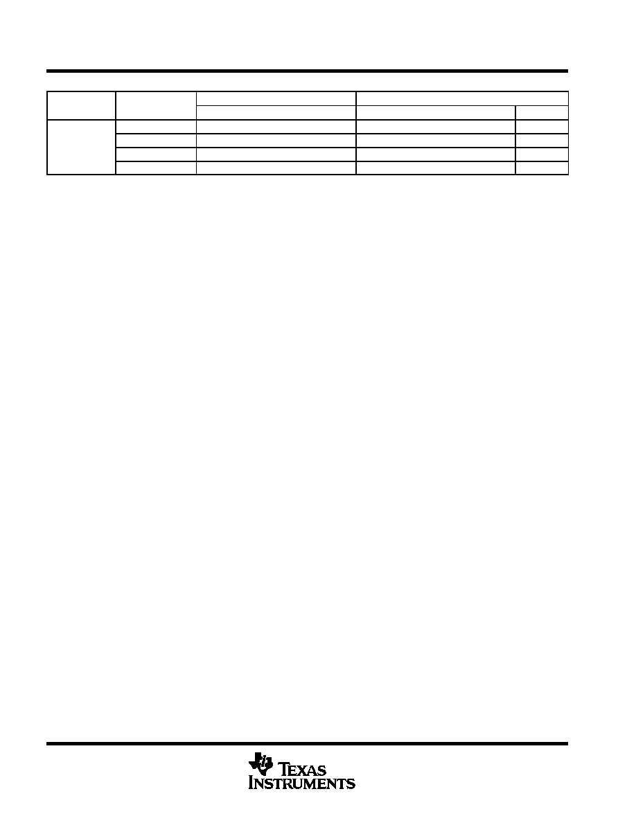
AVAILABLE OPTIONS
T
PACKAGES
NORMAL TO OVERCHARGE
OVERVOLTAGE TO NORMAL RECOVERY
TA
PACKAGES
BCC≠18 (GSH)
MIN
TYP
MAX
MIN
TYP
MAX
UNIT
UCC3952AGSH≠1
4.15
4.2
4.25
3.85
3.90
3.95
V
20
∞
C to 70
∞
C
UCC3952AGSH≠2
4.20
4.25
4.30
3.90
3.95
4.00
V
≠20
∞
C to 70
∞
C
UCC3952AGSH≠3
4.25
4.30
4.35
3.95
4.00
4.05
V
UCC3952AGSH≠4
4.30
4.35
4.40
4.00
4.05
4.10
V
absolute maximum ratings over operating free-air temperature (unless otherwise noted)
Supply voltage (PACK+ to BNEG)
7 V
. . . . . . . . . . . . . . . . . . . . . . . . . . . . . . . . . . . . . . . . . . . . . . . . . . . . . . . . . . . . .
Maximum forward voltage (PACK+ to PACK≠) 16
V
. . . . . . . . . . . . . . . . . . . . . . . . . . . . . . . . . . . . . . . . . . . . . . . . .
Maximum reverse voltage (where PACK+ to BNEG = 5V)
≠8 V
. . . . . . . . . . . . . . . . . . . . . . . . . . . . . . . . . . . . . . .
Maximum cell continuous charge current
3.5 A
. . . . . . . . . . . . . . . . . . . . . . . . . . . . . . . . . . . . . . . . . . . . . . . . . . . . .
Junction temperature, T
J
≠55
∞
C to 150
∞
C
. . . . . . . . . . . . . . . . . . . . . . . . . . . . . . . . . . . . . . . . . . . . . . . . . . . . . . . . . .
Storage temperature range, T
stg
≠65
∞
C to 150
∞
C
. . . . . . . . . . . . . . . . . . . . . . . . . . . . . . . . . . . . . . . . . . . . . . . . . . .
Stresses beyond those listed under "absolute maximum ratings" may cause permanent damage to the device. These are stress ratings only, and
functional operation of the device at these or any other conditions beyond those indicated under "recommended operating conditions" is not
implied. Exposure to absolute-maximum-rated conditions for extended periods may affect device reliability.
NOTE 1: Currents are positive into, negative out of the specified terminal. Consult Packaging Section of Data Book for thermal limitations and
considerations of packages. All voltages are referenced to GND.
UCC3952A-1, UCC3952A-2, UCC3952A-3, UCC3952A-4
SINGLE CELL LITHIUM ION BATTERY PROTECTION IC
SLUS463C ≠ AUGUST 2000 ≠ REVISED MARCH 2001
3
POST OFFICE BOX 655303
∑
DALLAS, TEXAS 75265
POST OFFICE BOX 1443
∑
HOUSTON, TEXAS 77251≠1443
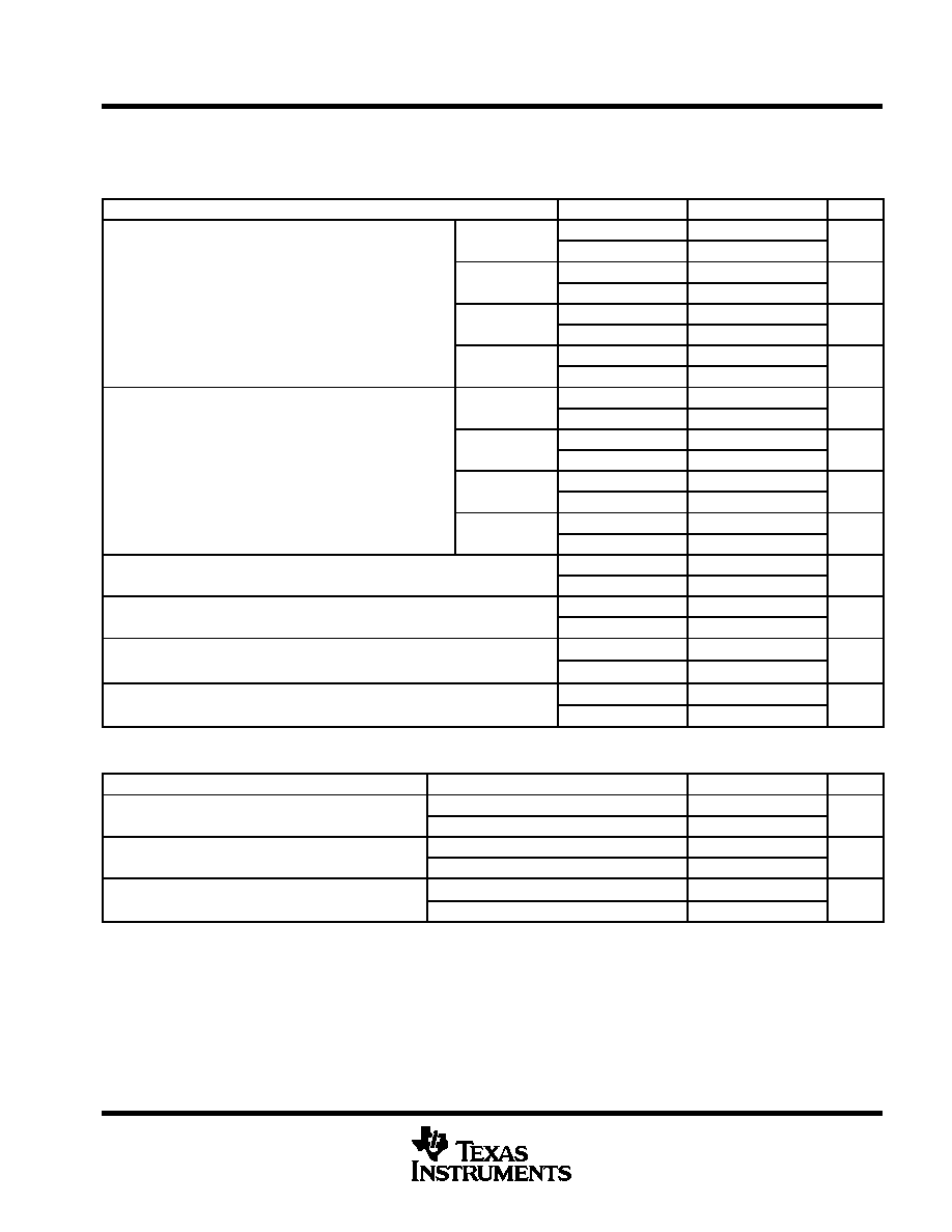
electrical characteristics, T
A
= ≠20
∞
C to 70
∞
C, all voltages are with respect to BNEG
(unless otherwise stated)
state transition threshold
PARAMETER
TEST CONDITIONS
MIN
TYP
MAX
UNITS
UCC3952A 1
4.15
4.20
4.25
V
UCC3952A≠1
TA = 25
∞
C
4.175
4.20
4.235
V
UCC3952A 2
4.20
4.25
4.30
V
V
Normal to o ercharge oltage
UCC3952A≠2
TA = 25
∞
C
4.225
4.25
4.285
V
VOV
Normal to overcharge voltage
UCC3952A 3
4.25
4.30
4.35
V
UCC3952A≠3
TA = 25
∞
C
4.275
4.30
4.335
V
UCC3952A 4
4.30
4.35
4.40
V
UCC3952A≠4
TA = 25
∞
C
4.325
4.35
4.385
V
UCC3952A 1
3.85
3.90
3.95
V
UCC3952A≠1
TA = 25
∞
C
3.87
3.90
3.94
V
UCC3952A 2
3.90
3.95
4.00
V
V
O ercharge to normal reco er
oltage
UCC3952A≠2
TA = 25
∞
C
3.92
3.95
3.99
V
VOVR
Overcharge to normal recovery voltage
UCC3952A 3
3.95
4.00
4.05
V
UCC3952A≠3
TA = 25
∞
C
3.97
4.00
4.04
V
UCC3952A 4
4.00
4.05
4.10
V
UCC3952A≠4
TA = 25
∞
C
4.02
4.05
4.09
V
V
Normal to ndercharge
2.25
2.35
2.45
V
VUV
Normal to undercharge
TA = 25
∞
C
2.26
2.35
2.44
V
V
Undercharge to normal reco er
2.55
2.65
2.75
V
VUVR
Undercharge to normal recovery
TA = 25
∞
C
2.57
2.65
2.73
V
tdOD
Overdischarge delay time
10
25
40
ms
tdOD
Overdischarge delay time
TA = 25
∞
C
13.5
25
36
ms
tdOV
Overvoltage delay time
1.0
1.75
2.5
s
tdOV
Overvoltage delay time
TA = 25
∞
C
1.15
1.75
2.3
s
short circuit protection
PARAMETER
TEST CONDITIONS
MIN
TYP
MAX
UNITS
I
Discharge current limit
PACK+ = 3.7 V
3.5
5
6.5
A
ITHLD
Discharge current limit
PACK+ = 3.7 V,
TA = 25
∞
C
3.8
5
6.3
A
t
Discharge c rrent dela
PACK+ = 3.7 V,
II = 6.5 A
1
2
3.0
ms
tdDLY
Discharge current delay
PACK+ = 3.7 V,
II = 6.5 A, TA = 25
∞
C
1.05
2
2.9
ms
RRESET
Discharge current reset resistance
PACK+ = 3.7 V
7.5
M
RRESET
Discharge current reset resistance
PACK+ = 3.7 V,
TA = 25
∞
C
7.4
M
UCC3952A-1, UCC3952A-2, UCC3952A-3, UCC3952A-4
SINGLE CELL LITHIUM ION BATTERY PROTECTION IC
SLUS463C ≠ AUGUST 2000 ≠ REVISED MARCH 2001
4
POST OFFICE BOX 655303
∑
DALLAS, TEXAS 75265
POST OFFICE BOX 1443
∑
HOUSTON, TEXAS 77251≠1443
electrical characteristics, T
A
= ≠20
∞
C to 70
∞
C, all voltages are with respect to BNEG (unless
otherwise stated) (continued)
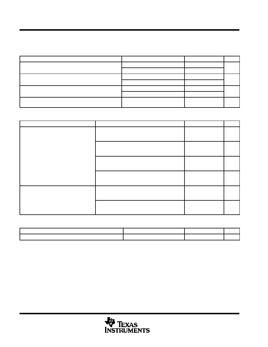
bias
PARAMETER
TEST CONDITIONS
MIN
TYP
MAX
UNITS
I
Supply current
VUV < VPACK < VOV
5
8
A
IDD
Supply current
VUV < VPACK < VOV, TA = 25
∞
C
5
7.5
µ
A
I
Operating s ppl c rrent in o er oltage
VOV < VPACK
11
24
A
IDDov
Operating supply current in overvoltage
V(OV) < V(PACK), TA = 25
∞
C
11
22
µ
A
I
Sh tdo n c rrent
V(PACK) = 2.0 V
2.5
A
ISD
Shutdown current
V(PACK) = 2.0 V, TA = 25
∞
C
2.25
µ
A
Vmin
Minimum cell voltage when all circuits are fully
functional
1.7
V
FET switch
PARAMETER
TEST CONDITIONS
MIN
TYP
MAX
UNITS
VPACK > VOV,
1 mA < ISWITCH < 2 A,
Battery overcharged state switch permits discharge
current only.
100
400
mV
V
Voltage at PACK
VPACK > VOV,
1 mA < ISWITCH < 2 A,
Battery overcharged state switch permits discharge
current only,
TA = 25
∞
C
100
350
mV
VPACK≠
Voltage at PACK≠
PACK+ = 2.5V,
≠2 mA < ISWITCH < ≠1 A,
Battery overdischarged state switch permits charge
current only.
≠600
≠100
mV
PACK+ = 2.5V,
≠2 mA < ISWITCH < ≠1 A,
Battery overdischarged state switch permits charge
current only,
TA = 25
∞
C
≠540
≠100
mV
R
Series resistance of the de ice
PACK+ = 2.5 V,
In normal mode (when not in OV or UV). This value
includes package and bondwire resistance.
60
80
m
RON
Series resistance of the device
PACK+ = 2.5 V,
TA = 25
∞
C
In normal mode (when not in OV or UV). This value
includes package and bondwire resistance.
60
70
m
thermal shutdown
PARAMETER
TEST CONDITIONS
MIN
TYP
MAX
UNITS
T(SD)
Thermal shutdown temperature (see Note 2)
135
∞
C
NOTE 2: This parameter is ensured by design and is not production tested.

UCC3952A-1, UCC3952A-2, UCC3952A-3, UCC3952A-4
SINGLE CELL LITHIUM ION BATTERY PROTECTION IC
SLUS463C ≠ AUGUST 2000 ≠ REVISED MARCH 2001
5
POST OFFICE BOX 655303
∑
DALLAS, TEXAS 75265
POST OFFICE BOX 1443
∑
HOUSTON, TEXAS 77251≠1443
APPLICATION INFORMATION
12
10
11
9
7
8
2
14
13
5
3
4
18
16
15
6
V
PUMP
TDLS
1 mS
SETD
RST
SYSTEM
CLOCK
GENERATOR
SEL
4≠1
MUX
V
UV
V
OV
V
UVR
V
OVR
THRESHOLD
COMPARATOR
THERMAL
SHUTDOWN
50 mV
50 mV
1.5 V
PACK+
CBPS
TCLK
BNEG
BNEG
BNEG
BNEG
BNEG
NC
PACK≠
PACK≠
PACK≠
PACK≠
NC
PACK≠
NC
T
DEL
1 SEC
T
DEL
10 mS
STATE
MACHINE
LOGIC
OV
UV
CLK
17
PACK+
1
NC
UDG≠98205
10 k
2 M
Figure 1. Detailed Block Diagram

UCC3952A-1, UCC3952A-2, UCC3952A-3, UCC3952A-4
SINGLE CELL LITHIUM ION BATTERY PROTECTION IC
SLUS463C ≠ AUGUST 2000 ≠ REVISED MARCH 2001
6
POST OFFICE BOX 655303
∑
DALLAS, TEXAS 75265
POST OFFICE BOX 1443
∑
HOUSTON, TEXAS 77251≠1443
pin descriptions
BNEG
Connect the negative terminal of the battery to this pin.
PACK+
Connect to the positive terminal of the battery. This pin is available to the user.
CBPS
This power supply bypass pin is connected to PACK+ through an internal 3-k
resistor. An external 0.1-
µ
F
capacitor must be connected between this pin and BNEG.
PACK≠
The negative terminal of the battery pack (negative terminal available to the user). The internal FET switch
connects this terminal to the BNEG terminal to give the battery pack user appropriate access to the battery. In
an overcharged state, only discharge current is permitted. In an overdischarged state, only charge current is
permitted.
TCLK
Production test mode pin. This pin is used to provide a high-frequency clock to the IC during production testing.
In an application, this pin is left unconnected or tied to BNEG.

UCC3952A-1, UCC3952A-2, UCC3952A-3, UCC3952A-4
SINGLE CELL LITHIUM ION BATTERY PROTECTION IC
SLUS463C ≠ AUGUST 2000 ≠ REVISED MARCH 2001
7
POST OFFICE BOX 655303
∑
DALLAS, TEXAS 75265
POST OFFICE BOX 1443
∑
HOUSTON, TEXAS 77251≠1443
APPLICATION INFORMATION
battery voltage monitoring
The battery cell voltage is sampled by connecting a resistor divider across it and comparing the resulting voltage
to a precision internal reference voltage. Under normal conditions (cell voltage is below the overvoltage
threshold and above the undervoltage threshold), the UCC3952A consumes less than 8
µ
A of current and the
internal MOSFET is fully turned on with the aid of a charge pump.
When the cell voltage falls below the undervoltage threshold for two consecutive samples, the IC disconnects
the load from the battery pack and enters a super-low-power mode. The pack remains in this state until it detects
the application of a charger, at which point charging is enabled. The requirement of two consecutive readings
below the undervoltage threshold filters out momentary drops in cell voltage due to load transients, preventing
nuisance trips.
If the cell voltage exceeds the overvoltage threshold for the overcharge delay time, charging is disabled;
however, discharge current is still allowed. This feature of the IC is explained further in the controlled
charge/discharge mode section of this document.
overcurrent monitoring and protection
Discharge current is continuously monitored via an internal sense resistor. In the event of excessive current,
an overcurrent condition is declared if the high current persists for t
dDLY
. This delay allows for charging of the
system bypass capacitors without tripping the overcurrent protection. A 0.1-
µ
F capacitor on the CBPS pin
provides momentary holdup for the IC to assure proper operation in the event that a hard short suddenly pulls
the cell voltage below the minimum operating voltage.
Once the overcurrent condition has been declared, the internal MOSFET turns off. To return the device to normal
operation, the UCC3952A needs to have a load impedance greater than 7.5 M
placed across PACK+ to
PACK≠. This typically can be achieved by removing the battery pack from the system. At this point, the pack
returns to its normal state of operation.
controlled charge/discharge mode
When the chip senses an overvoltage condition, it prevents any additional charging, but allows discharge. This
is accomplished by activating a linear control loop, which controls the gate of the MOSFET based on the
differential voltage across its drain-to-source terminals. The linear loop attempts to regulate the differential
voltage across the MOSFET to 100 mV. When a light load is applied to the part, the loop adjusts the impedance
of the MOSFET to maintain 100 mV across it. As the load increases, the impedance of the MOSFET is
decreased to maintain the 100-mV control. At heavy loads (still below the overcurrent limit), the loop does not
maintain regulation and drives the gate of the MOSFET to the battery voltage (not the charge-pump output
voltage). The MOSFET R
DS(on)
in the overvoltage state is higher than R
DS(on)
during normal operation. The
voltage drop (and associated power loss) across the internal MOSFET in this mode of operation is still
significantly lower than the typical solution of two external back-to-back MOSFETs, where the body diode is
conducting.
When the chip senses an undervoltage condition, it disconnects the load from the battery pack and shuts itself
down to minimize current drain from the battery. Several circuits remain powered and detect placement of the
battery pack into a charger. Once the charger presence is detected, the linear loop is activated and the chip
allows charging current into the battery. This linear control mode of operation is in effect until the battery voltage
reaches a level of V
UVR
, at which time normal operation is resumed.
UCC3952A-1, UCC3952A-2, UCC3952A-3, UCC3952A-4
SINGLE CELL LITHIUM ION BATTERY PROTECTION IC
SLUS463C ≠ AUGUST 2000 ≠ REVISED MARCH 2001
8
POST OFFICE BOX 655303
∑
DALLAS, TEXAS 75265
POST OFFICE BOX 1443
∑
HOUSTON, TEXAS 77251≠1443
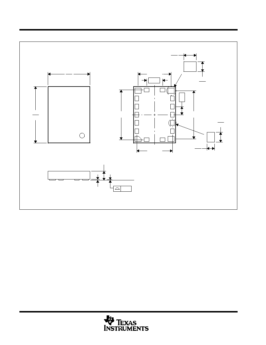
GSH (R-PLGA-N18)
PLASTIC LAND GRID ARRAY
0,65
0,05
1,30
4200956/A 07/00
3,50
3,30
0,80 MAX
0,10 MAX
Seating Plane
0,40
0,20
0,30
0,50
4,65
4,45
2,70 TYP
4,05 TYP
3,90 TYP
0,50
0,30
0,40
0,60
2,90 TYP
NOTES: A. All linear dimensions are in millimeters.
B. This drawing is subject to change without notice.

IMPORTANT NOTICE
Texas Instruments and its subsidiaries (TI) reserve the right to make changes to their products or to discontinue
any product or service without notice, and advise customers to obtain the latest version of relevant information
to verify, before placing orders, that information being relied on is current and complete. All products are sold
subject to the terms and conditions of sale supplied at the time of order acknowledgment, including those
pertaining to warranty, patent infringement, and limitation of liability.
TI warrants performance of its products to the specifications applicable at the time of sale in accordance with
TI's standard warranty. Testing and other quality control techniques are utilized to the extent TI deems necessary
to support this warranty. Specific testing of all parameters of each device is not necessarily performed, except
those mandated by government requirements.
Customers are responsible for their applications using TI components.
In order to minimize risks associated with the customer's applications, adequate design and operating
safeguards must be provided by the customer to minimize inherent or procedural hazards.
TI assumes no liability for applications assistance or customer product design. TI does not warrant or represent
that any license, either express or implied, is granted under any patent right, copyright, mask work right, or other
intellectual property right of TI covering or relating to any combination, machine, or process in which such
products or services might be or are used. TI's publication of information regarding any third party's products
or services does not constitute TI's approval, license, warranty or endorsement thereof.
Reproduction of information in TI data books or data sheets is permissible only if reproduction is without
alteration and is accompanied by all associated warranties, conditions, limitations and notices. Representation
or reproduction of this information with alteration voids all warranties provided for an associated TI product or
service, is an unfair and deceptive business practice, and TI is not responsible nor liable for any such use.
Resale of TI's products or services with
statements different from or beyond the parameters stated by TI for
that product or service voids all express and any implied warranties for the associated TI product or service,
is an unfair and deceptive business practice, and TI is not responsible nor liable for any such use.
Also see: Standard Terms and Conditions of Sale for Semiconductor Products. www.ti.com/sc/docs/stdterms.htm
Mailing Address:
Texas Instruments
Post Office Box 655303
Dallas, Texas 75265
Copyright
2001, Texas Instruments Incorporated