
UCC3952-1, UCC3952-2, UCC3952-3, UCC3952-4
Single Cell Lithium Ion Battery Protection IC
SLUS400D ≠ AUGUST 2000
1
POST OFFICE BOX 655303
∑
DALLAS, TEXAS 75265
D
Protects Sensitive Lithium-Ion Cells From
Overcharging and Over-Discharging
D
Dedicated for One-Cell Applications
D
Integrated Low-Impedance MOSFET Switch
and Sense Resistor
D
Precision Trimmed Overcharge and
Overdischarge Voltage Limits
D
Extremely Low Power Drain
D
3-A Current Capacity
D
Overcurrent and Short-Circuit Protection
D
Reverse Charger Protection
D
Thermal Protection
description
The UCC3952 monolithic BiCMOS lithium≠ion
battery protection circuit increases the useful
operating life of a one-cell rechargeable battery
pack. Cell protection features include internally
trimmed charge and discharge voltage limits,
discharge current limit with a delayed shutdown,
and an ultra-low-current sleep mode state when
the cell is discharged. Additional features include
an on-chip MOSFET for reduced external compo-
nent count and a charge pump for reduced power
losses while charging or discharging a low-cell-
voltage battery pack. This protection circuit
requires one external capacitor and can operate
and safely shut down in a short circuit condition.
Copyright
©
2000, Texas Instruments Incorporated
PRODUCTION DATA information is current as of publication date.
Products conform to specifications per the terms of Texas Instruments
standard warranty. Production processing does not necessarily include
testing of all parameters.
Please be aware that an important notice concerning availability, standard warranty, and use in critical applications of
Texas Instruments semiconductor products and disclaimers thereto appears at the end of this data sheet.
1
2
3
4
5
6
7
8
16
15
14
13
12
11
10
9
TCLK
NC
BNEG
BNEG
BNEG
BNEG
BNEG
BNEG
PACK+
CBPS
NC
PACK≠
PACK≠
PACK≠
PACK≠
PACK≠
PW PACKAGE
(TOP VIEW)
1
2
3
4
5
6
7
8
16
15
14
13
12
11
10
9
DP PACKAGE
(TOP VIEW)
TCLK
NC
NC
SUB
SUB
BNEG
BNEG
BNEG
PACK+
CBPS
NC
SUB
SUB
PACK≠
PACK≠
PACK≠

UCC3952-1, UCC3952-2, UCC3952-3, UCC3952-4
Single Cell Lithium Ion Battery Protection IC
SLUS400D ≠ AUGUST 2000
2
POST OFFICE BOX 655303
∑
DALLAS, TEXAS 75265
application diagram
1
3
2
4
5
7
6
8
16
14
15
13
12
10
11
9
0.1
µ
F
3 k
TCLK
N/C
BNEG
BNEG
BNEG
BNEG
BNEG
BNEG
PACK ≠
NC
CBPS
PACK +
LOAD
CHARGER
+
PACK ≠
PACK ≠
PACK ≠
PACK ≠
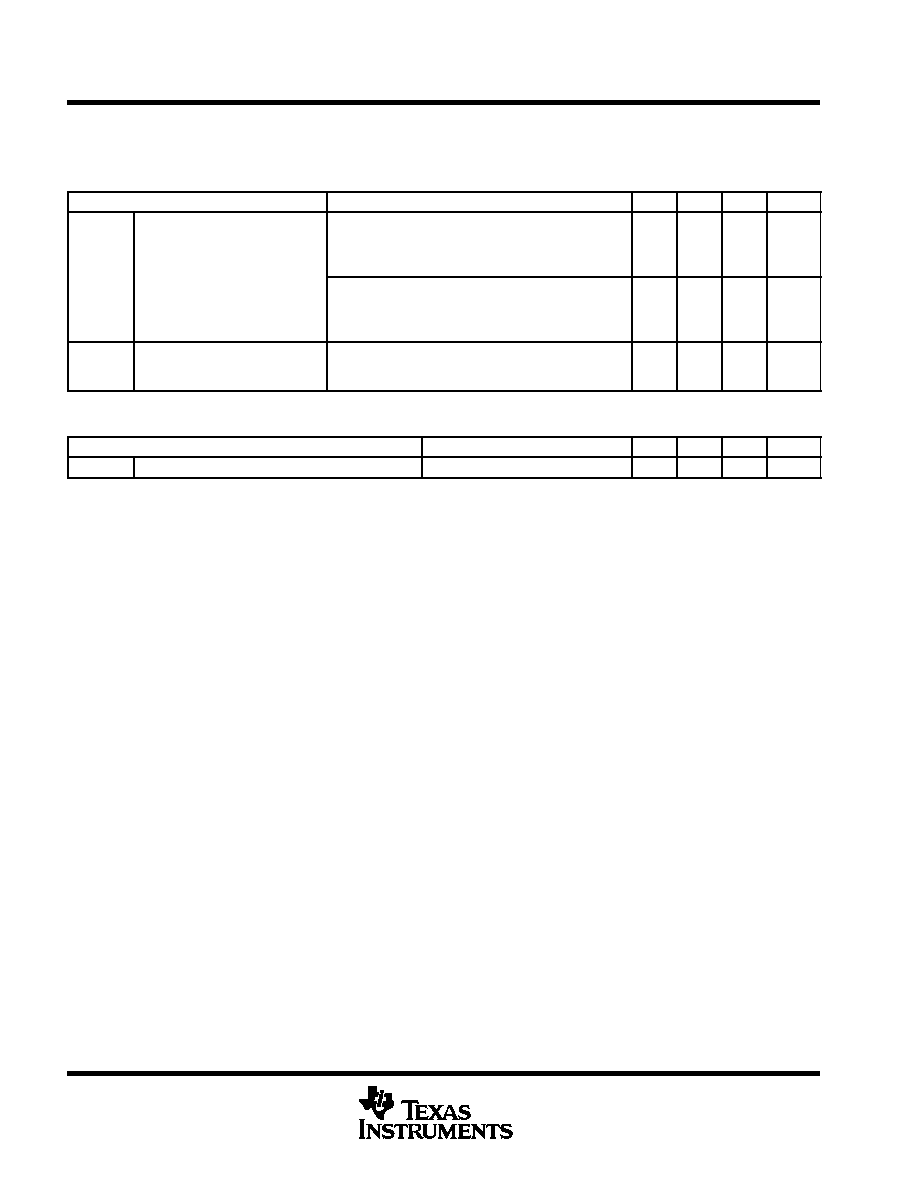
AVAILABLE OPTIONS
PACKAGES
TA
TSSOP≠16 (PW)
SOIC≠16 (DP)
UCC3952PW≠1
UCC3952DP≠1
≠20
∞
C to 70
∞
C
UCC3952PW≠2
UCC3952DP≠2
≠20
∞
C to 70
∞
C
UCC3952PW≠3
UCC3952DP≠3
UCC3952PW≠4
UCC3952DP≠4

UCC3952-1, UCC3952-2, UCC3952-3, UCC3952-4
Single Cell Lithium Ion Battery Protection IC
SLUS400D ≠ AUGUST 2000
3
POST OFFICE BOX 655303
∑
DALLAS, TEXAS 75265
absolute maximum ratings over operating free-air temperature (unless otherwise noted)
Supply voltage (PACK+ to BNEG)
7 V
. . . . . . . . . . . . . . . . . . . . . . . . . . . . . . . . . . . . . . . . . . . . . . . . . . . . . . . . . . . . .
Maximum forward voltage (PACK+ to PACK≠)
16 V
. . . . . . . . . . . . . . . . . . . . . . . . . . . . . . . . . . . . . . . . . . . . . . . . .
Maximum reverse voltage (where PACK+ to BNEG = 5V)
≠8 V
. . . . . . . . . . . . . . . . . . . . . . . . . . . . . . . . . . . . . . .
Maximum cell continuous charge current
3 A
. . . . . . . . . . . . . . . . . . . . . . . . . . . . . . . . . . . . . . . . . . . . . . . . . . . . . . .
Junction temperature, T
J
≠55
∞
C to 150
∞
C
. . . . . . . . . . . . . . . . . . . . . . . . . . . . . . . . . . . . . . . . . . . . . . . . . . . . . . . . . .
Storage Temperature range, T
stg
≠65
∞
C to 150
∞
C
. . . . . . . . . . . . . . . . . . . . . . . . . . . . . . . . . . . . . . . . . . . . . . . . . . .
Stresses beyond those listed under "absolute maximum ratings" may cause permanent damage to the device. These are stress ratings only, and
functional operation of the device at these or any other conditions beyond those indicated under "recommended operating conditions" is not
implied. Exposure to absolute-maximum-rated conditions for extended periods may affect device reliability.
NOTE 1: Currents are positive into, negative out of the specified terminal. Consult Packaging Section of Data Book for thermal limitations and
considerations of packages. All voltages are referenced to GND.
electrical characteristics, T
A
= ≠20
∞
C to 70
∞
C, all voltages are with respect to BNEG (unless
otherwise stated)
state transition threshold
PARAMETER
TEST CONDITIONS
MIN
TYP
MAX
UNITS
UCC3952≠1
4.15
4.20
4.25
V
Normal to overcharge voltage
UCC3952≠2
4.20
4.25
4.30
V
V(OV)
Normal to overcharge voltage
UCC3952≠3
4.25
4.30
4.35
V
UCC3952≠4
4.30
4.35
4.40
UCC3952≠1
3.85
3.90
3.95
V
Overcharge to normal recovery
UCC3952≠2
3.90
3.95
4.00
V
V(OVR)
Overcharge to normal recovery
voltage
UCC3952≠3
3.95
4.00
4.05
V
g
UCC3952≠4
4.00
4.05
4.10
V(UV)
Normal to undercharge
2.25
2.35
2.45
V
V(UVR)
Undercharge to normal recovery
2.55
2.65
2.75
V
td(OD)
Overcharge delay time
10
25
40
ms
short circuit protection
PARAMETER
TEST CONDITIONS
MIN
TYP
MAX
UNITS
I(THLD)
Discharge current limit
PACK+ = 3.7 V
3.0
6.0
A
td(DLY)
Discharge current delay
PACK+ = 3.7 V, II = 6 A
1
3.0
ms
R(RESET)
Discharge current reset resistance
PACK+ = 3.7 V
7.5
M
bias
PARAMETER
TEST CONDITIONS
MIN
TYP
MAX
UNITS
IDD
Supply current
V(UV) < V(PACK) < V(OV)
5
8
µ
A
IDD(OV)
Operating supply current in overvoltage
V(OV) < V(PACK)
11
24
µ
A
I(SD)
Shutdown current
V(PACK) = 2.0 V
2.5
µ
A
V(min)
Minimum cell voltage when all circuits are fully
functional
1.7
V
td(OV)
Overvoltage delay time
1
2
s
UCC3952-1, UCC3952-2, UCC3952-3, UCC3952-4
Single Cell Lithium Ion Battery Protection IC
SLUS400D ≠ AUGUST 2000
4
POST OFFICE BOX 655303
∑
DALLAS, TEXAS 75265
electrical characteristics, T
A
= ≠20
∞
C to 70
∞
C, all voltages are with respect to BNEG (unless
otherwise stated) (continued)
FET switch
PARAMETER
TEST CONDITIONS
MIN
TYP
MAX
UNITS
V
Voltage at PACK
PACK+ > VOV ,
I(SWITCH) = 1 mA to 2 A,
Battery overcharged state switch permits discharge
current only.
100
400
mV
V(PACK≠)
Voltage at PACK≠
PACK+ = 2.5V,
I(SWITCH) = ≠1 mA to ≠2 A,
Battery overdischarged state switch permits charge
current only.
≠600
≠100
mV
RON
Series resistance of the device
PACK+ = 2.5 V,
In normal mode (when not in OV or UV). This value
includes package and bondwire resistance.
50
75
m
thermal shutdown
PARAMETER
TEST CONDITIONS
MIN
TYP
MAX
UNITS
T(SD)
Thermal shutdown temperature (see Note 2)
135
∞
C
NOTE 2: This parameter is ensured by design and is not production tested.
detailed description
pin descriptions
BNEG
Connect the negative terminal of the battery to this pin.
PACK+
Connect to the positive terminal of the battery. This pin is available to the user.
CBPS
This power supply bypass pin is connected to PACK+ through an internal 3-k
resistor. An external 0.1-
µ
F
capacitor must be connected between this pin and BNEG.
PACK≠
The negative terminal of the battery pack (negative terminal available to the user). The internal FET switch
connects this terminal to the BNEG terminal to give the battery pack user appropriate access to the battery. In
an overcharged state, only discharge current is permitted. In an overdischarged state, only charge current is
permitted.
SUB (DP Package Only)
Do not connect. These pins must be electrically isolated from all other pins. The SUB pins may be soldered to
an isolated copper pad for heatsinking. However, most applications do not require heatsinking.
TCLK
Production test mode pin. This pin is used to provide a high-frequency clock to the IC during production testing.
In an application, this pin is left unconnected or tied to BNEG.
UCC3952-1, UCC3952-2, UCC3952-3, UCC3952-4
Single Cell Lithium Ion Battery Protection IC
SLUS400D ≠ AUGUST 2000
5
POST OFFICE BOX 655303
∑
DALLAS, TEXAS 75265
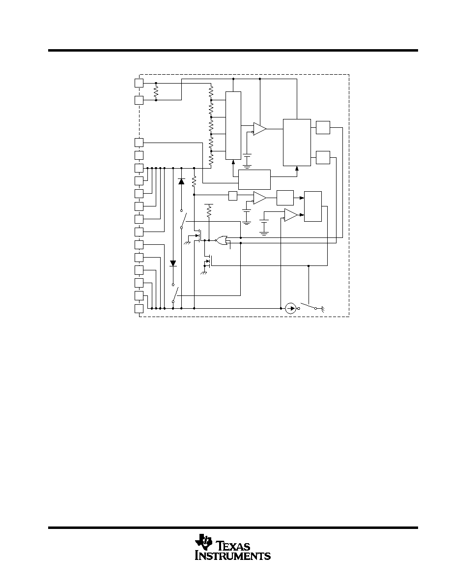
APPLICATION INFORMATION
12
10
11
9
7
8
2
14
5
3
4
1
16
15
6
V
PUMP
TDLS
1mS
SETD
RST
SYSTEM
CLOCK
GENERATOR
SEL
4≠1
MUX
V
UV
V
OV
V
UVR
V
OVR
THRESHOLD
COMPARATOR
THERMAL
SHUTDOWN
50mV
50mV
2M
3k
1.5V
PACK+
CBPS
TCLK
BNEG
BNEG
BNEG
BNEG
BNEG
BNEG
PACK≠
PACK≠
PACK≠
PACK≠
PACK≠
NC
N/C
T
DEL
1SEC
T
DEL
10mS
STATE
MACHINE
LOGIC
OV
UV
CLK
13
Figure 1. Detailed Block Diagram
battery voltage monitoring
The battery cell voltage is sampled every 8 ms by connecting a resistor divider across it and comparing the
resulting voltage to a precision internal reference voltage. Under normal conditions (cell voltage is below
overvoltage threshold and above undervoltage threshold), the UCC3952 consumes less than 10
µ
A of current
and the internal MOSFET is fully turned on with the aid of a charge pump.
When the cell voltage falls below the undervoltage threshold for two consecutive samples, the IC disconnects
the load from the battery pack and enters a super-low-power mode. The pack remains in this state until it detects
the application of a charger, at which point charging is enabled. The requirement of two consecutive readings
below the undervoltage threshold filters out momentary drops in cell voltage due to load transients, preventing
nuisance trips.
If the cell voltage exceeds the overvoltage threshold for 1 second, charging is disabled; however, discharge
current is still allowed. This feature of the IC is explained further in the
controlled charge/discharge mode section
of this document.

UCC3952-1, UCC3952-2, UCC3952-3, UCC3952-4
Single Cell Lithium Ion Battery Protection IC
SLUS400D ≠ AUGUST 2000
6
POST OFFICE BOX 655303
∑
DALLAS, TEXAS 75265
APPLICATION INFORMATION
overcurrent monitoring and protection
Discharge current is continuously monitored via an internal sense resistor. In the event of excessive current,
an overcurrent condition is declared if the high current (over 3 A) persists for over 1 ms. This delay allows for
charging of the system bypass capacitors without tripping the overcurrent protection. A 0.1-
µ
F capacitor on the
CBPS pin provides momentary holdup for the IC to assure proper operation in the event that a hard short
suddenly pulls the cell voltage below the minimum operating voltage.
Once an overcurrent condition has been declared, the internal MOSFET turns off. To return the device to normal
operation, the UCC3952 requires a load impedance greater than 7.5 M
across PACK+ to PACK≠. This
impedance is typically achieved by removing the battery pack from the system. At this point, the pack returns
to its normal state of operation.
controlled charge/discharge mode
When the chip senses an overvoltage condition, it prevents any additional charging, but allows discharge. This
is accomplished by activating a linear control loop, which controls the gate of the MOSFET based on the
differential voltage across its drain-to-source terminals. The linear loop attempts to regulate the differential
voltage across the MOSFET to 100 mV. When a light load is applied to the part, the loop adjusts the impedance
of the MOSFET to maintain 100 mV across it. As the load increases, the impedance of the MOSFET is
decreased to maintain the 100-mV control. At heavy loads (still below the overcurrent limit), the loop does not
maintain regulation and drives the gate of the MOSFET to the battery voltage (not the charge-pump output
voltage). The MOSFET R
DS(on)
in the overvoltage state is higher than RDS(on) during normal operation. The
voltage drop (and associated power loss) across the internal MOSFET in this mode of operation is still
significantly lower than the typical solution of two external back-to-back MOSFETs, where the body diode is
conducting.
When the chip senses an undervoltage condition, it disconnects the load from the battery pack and shuts itself
down to minimize current drain from the battery. Several circuits remain powered and detect placement of the
battery pack into a charger. Once the charger presence is detected, the linear loop is activated and the chip
allows charging current into the battery. This linear control mode of operation is in effect until the battery voltage
reaches a level of V
UVR
, at which time normal operation is resumed.
PACKAGING INFORMATION
Orderable Device
Status
(1)
Package
Type
Package
Drawing
Pins Package
Qty
Eco Plan
(2)
Lead/Ball Finish
MSL Peak Temp
(3)
UCC3952DP-1
ACTIVE
SOIC
D
16
40
None
CU SNPB
Level-1-220C-UNLIM
UCC3952DP-2
ACTIVE
SOIC
D
16
40
None
CU SNPB
Level-1-220C-UNLIM
UCC3952DP-3
ACTIVE
SOIC
D
16
40
None
CU SNPB
Level-1-220C-UNLIM
UCC3952DP-4
ACTIVE
SOIC
D
16
40
None
CU SNPB
Level-1-220C-UNLIM
UCC3952PW-1
ACTIVE
TSSOP
PW
16
90
None
CU NIPDAU
Level-2-220C-1 YEAR
UCC3952PW-2
ACTIVE
TSSOP
PW
16
90
None
CU NIPDAU
Level-2-220C-1 YEAR
UCC3952PW-3
ACTIVE
TSSOP
PW
16
90
None
CU NIPDAU
Level-2-220C-1 YEAR
UCC3952PW-4
ACTIVE
TSSOP
PW
16
90
None
CU NIPDAU
Level-2-220C-1 YEAR
UCC3952PWTR-1
ACTIVE
TSSOP
PW
16
2000
None
CU NIPDAU
Level-2-220C-1 YEAR
UCC3952PWTR-2
ACTIVE
TSSOP
PW
16
2000
None
CU NIPDAU
Level-2-220C-1 YEAR
UCC3952PWTR-3
ACTIVE
TSSOP
PW
16
2000
None
CU NIPDAU
Level-2-220C-1 YEAR
UCC3952PWTR-4
ACTIVE
TSSOP
PW
16
2000
None
CU NIPDAU
Level-2-220C-1 YEAR
(1)
The marketing status values are defined as follows:
ACTIVE: Product device recommended for new designs.
LIFEBUY: TI has announced that the device will be discontinued, and a lifetime-buy period is in effect.
NRND: Not recommended for new designs. Device is in production to support existing customers, but TI does not recommend using this part in
a new design.
PREVIEW: Device has been announced but is not in production. Samples may or may not be available.
OBSOLETE: TI has discontinued the production of the device.
(2)
Eco Plan - May not be currently available - please check
http://www.ti.com/productcontent
for the latest availability information and additional
product content details.
None: Not yet available Lead (Pb-Free).
Pb-Free (RoHS): TI's terms "Lead-Free" or "Pb-Free" mean semiconductor products that are compatible with the current RoHS requirements
for all 6 substances, including the requirement that lead not exceed 0.1% by weight in homogeneous materials. Where designed to be soldered
at high temperatures, TI Pb-Free products are suitable for use in specified lead-free processes.
Green (RoHS & no Sb/Br): TI defines "Green" to mean "Pb-Free" and in addition, uses package materials that do not contain halogens,
including bromine (Br) or antimony (Sb) above 0.1% of total product weight.
(3)
MSL, Peak Temp. -- The Moisture Sensitivity Level rating according to the JEDECindustry standard classifications, and peak solder
temperature.
Important Information and Disclaimer:The information provided on this page represents TI's knowledge and belief as of the date that it is
provided. TI bases its knowledge and belief on information provided by third parties, and makes no representation or warranty as to the
accuracy of such information. Efforts are underway to better integrate information from third parties. TI has taken and continues to take
reasonable steps to provide representative and accurate information but may not have conducted destructive testing or chemical analysis on
incoming materials and chemicals. TI and TI suppliers consider certain information to be proprietary, and thus CAS numbers and other limited
information may not be available for release.
In no event shall TI's liability arising out of such information exceed the total purchase price of the TI part(s) at issue in this document sold by TI
to Customer on an annual basis.
PACKAGE OPTION ADDENDUM
www.ti.com
11-Mar-2005
Addendum-Page 1

IMPORTANT NOTICE
Texas Instruments Incorporated and its subsidiaries (TI) reserve the right to make corrections, modifications,
enhancements, improvements, and other changes to its products and services at any time and to discontinue
any product or service without notice. Customers should obtain the latest relevant information before placing
orders and should verify that such information is current and complete. All products are sold subject to TI's terms
and conditions of sale supplied at the time of order acknowledgment.
TI warrants performance of its hardware products to the specifications applicable at the time of sale in
accordance with TI's standard warranty. Testing and other quality control techniques are used to the extent TI
deems necessary to support this warranty. Except where mandated by government requirements, testing of all
parameters of each product is not necessarily performed.
TI assumes no liability for applications assistance or customer product design. Customers are responsible for
their products and applications using TI components. To minimize the risks associated with customer products
and applications, customers should provide adequate design and operating safeguards.
TI does not warrant or represent that any license, either express or implied, is granted under any TI patent right,
copyright, mask work right, or other TI intellectual property right relating to any combination, machine, or process
in which TI products or services are used. Information published by TI regarding third-party products or services
does not constitute a license from TI to use such products or services or a warranty or endorsement thereof.
Use of such information may require a license from a third party under the patents or other intellectual property
of the third party, or a license from TI under the patents or other intellectual property of TI.
Reproduction of information in TI data books or data sheets is permissible only if reproduction is without
alteration and is accompanied by all associated warranties, conditions, limitations, and notices. Reproduction
of this information with alteration is an unfair and deceptive business practice. TI is not responsible or liable for
such altered documentation.
Resale of TI products or services with statements different from or beyond the parameters stated by TI for that
product or service voids all express and any implied warranties for the associated TI product or service and
is an unfair and deceptive business practice. TI is not responsible or liable for any such statements.
Following are URLs where you can obtain information on other Texas Instruments products and application
solutions:
Products
Applications
Amplifiers
amplifier.ti.com
Audio
www.ti.com/audio
Data Converters
dataconverter.ti.com
Automotive
www.ti.com/automotive
DSP
dsp.ti.com
Broadband
www.ti.com/broadband
Interface
interface.ti.com
Digital Control
www.ti.com/digitalcontrol
Logic
logic.ti.com
Military
www.ti.com/military
Power Mgmt
power.ti.com
Optical Networking
www.ti.com/opticalnetwork
Microcontrollers
microcontroller.ti.com
Security
www.ti.com/security
Telephony
www.ti.com/telephony
Video & Imaging
www.ti.com/video
Wireless
www.ti.com/wireless
Mailing Address:
Texas Instruments
Post Office Box 655303 Dallas, Texas 75265
Copyright
2005, Texas Instruments Incorporated