 | –≠–ª–µ–∫—Ç—Ä–æ–Ω–Ω—ã–π –∫–æ–º–ø–æ–Ω–µ–Ω—Ç: UCC5614N | –°–∫–∞—á–∞—Ç—å:  PDF PDF  ZIP ZIP |
UCC5614
SLUS349A ≠ DECEMBER 1994 ≠ REVISED APRIL 2003
9 LINE 3 TO 5 VOLT LOW CAPACITANCE SCSI ACTIVE TERMINATOR
1
www.ti.com
FEATURES
D
Complies with SCSI, SCSI≠2 and SPI≠2 Single
Ended Standards
D
2.7-V to 5.25-V Operation
D
1.8-pF Channel Capacitance during
Disconnect
D
0.5-
µ
A Supply Current in Disconnect Mode
D
110-
/2.5-k
Programmable Termination
D
Completely Meets SCSI Hot Plugging
D
≠400-mA Sourcing Current for Termination
D
+400-mA Sinking Current for Active Negation
Drivers
D
Trimmed Termination Current to 4%
D
Trimmed Impedance to 7%
D
Current Limit and Thermal Shutdown
Protection
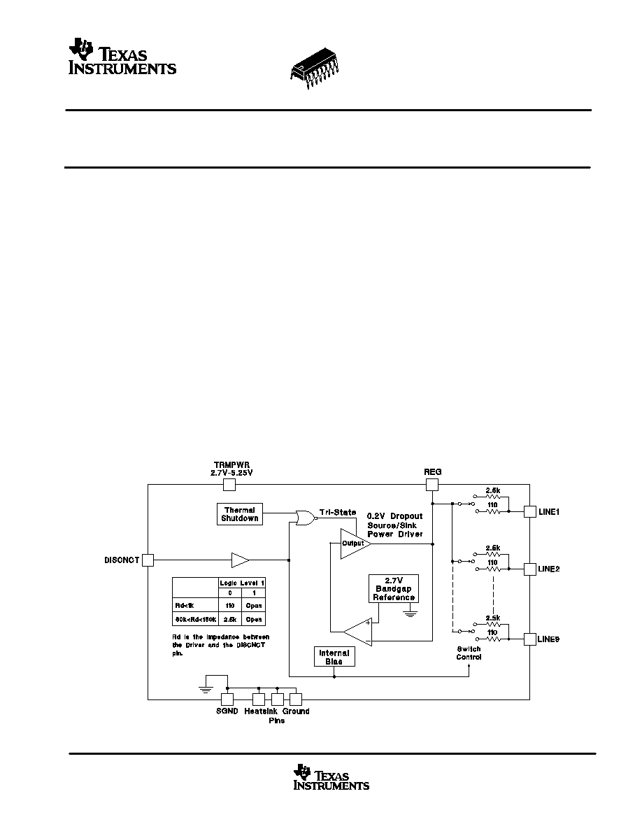
DESCRIPTION
The UCC5614 provides 9 lines of active termination for
a small computer system's interface (SCSI) parallel
bus. The SCSI standard recommends active
termination at both ends of the cable segment.
The UCC5614 is ideal for high performance 3.3-V SCSI
systems. The key features contributing to such low
operating voltage are the 0.1-V drop-out regulator and
the 2.7-V reference. During disconnect the supply
current is typically only 0.5
µ
A, which makes the device
attractive for battery powered systems.
The UCC5614 is designed with an ultra low channel
capacitance of 1.8 pF, which eliminates effects on signal
integrity from disconnected terminators at interim points
on the bus.
BLOCK DIAGRAM
PRODUCTION DATA information is current as of publication date.
Products conform to specifications per the terms of Texas Instruments
standard warranty. Production processing does not necessarily include
testing of all parameters.
Copyright
2003, Texas Instruments Incorporated
UCC5614
SLUS349A ≠ DECEMBER 1994 ≠ REVISED APRIL 2003
2
www.ti.com
DESCRIPTION (CONTINUED)
The UCC5614 can be programmed for either a 110-
or 2.5-k
termination. The 110-
termination is used for
standard SCSI bus lengths and the 2.5-k
termination is typically used in short bus applications. When driving
the TTL compatible DISCNCT pin directly, the 110-
termination is connected when the DISCNCT pin is driven
low, and disconnected when driven high. When the DISCNCT pin is driven through an impedance between
80 k
and 150 k
,
the terminator is in short bus mode. The 2.5-k
termination is connected when the DISCNCT
pin is driven low and disconnected when driven high.
The power amplifier output stage allows the UCC5614 to source full termination current and sink active negation
current when all termination lines are actively negated.
The UCC5614 is pin for pin compatible with Unitrode's other 9-line SCSI terminators, allowing lower capacitance
and lower voltage upgrades to existing systems. The UCC5614, as with all Unitrode terminators, is completely
hot pluggable and appears as high impedance at the terminating channels with VTRMPWR = 0 V or open.
Internal circuit trimming is utilized, first to trim the 110-
termination impedance to a 7% tolerance, and then most
importantly, to trim the output current to a 4% tolerance, as close to the max SCSI specification as possible,
which maximizes noise margin in fast SCSI operation.
Other features include thermal shutdown and current limit.
This device is offered in low thermal resistance versions of the industry standard 16-pin narrow body SOIC,
16-pin N and 24-pin TSSOP.
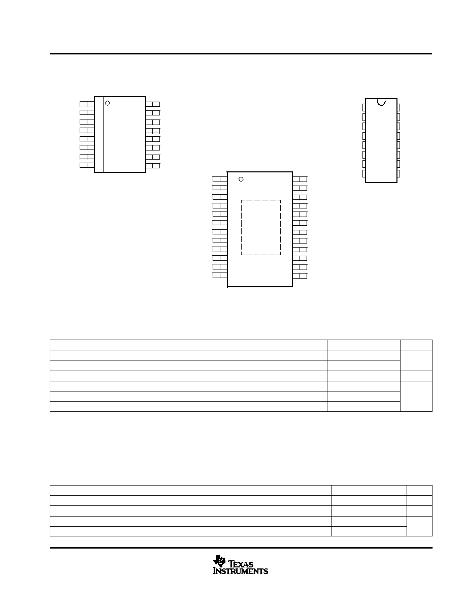
ORDERING INFORMATION
T
PACKAGED DEVICE
TA
SOIC-16 (DP)
{
DIL-16 (N)
TSSOP-24 (PWP)
}
0
∞
C to 70
∞
C
UCC5614DP
UCC5614N
UCC5614PWP
The DP package is available taped and reeled in quanities of 2,500. Add TR suffix to device type (e.g. UCC5614DPTR) to order quantities of
2,500 devices per reel.
The PWP package is available taped and reeled in quanities of 2,000. Add TR suffix to device type (e.g. UCC5614PWPTR) to order quantities
of 2,000 devices per reel.
UCC5614
SLUS349A ≠ DECEMBER 1994 ≠ REVISED APRIL 2003
3
www.ti.com
CONNECTION DIAGRAMS
1
2
3
4
5
6
7
8
16
15
14
13
12
11
10
9
LINE7
LINE8
LINE9
GND
SGND
DISCNCT
LINE1
LINE2
LINE6
LINE5
REG
GND
GND
TRMPWR
LINE4
LINE3
1
2
3
4
5
6
7
8
16
15
14
13
12
11
10
9
LINE7
LINE8
LINE9
N/C
SGND
DISCNCT
LINE1
LINE2
LINE6
LINE5
REG
N/C
N/C
TRMPWR
LINE4
LINE3
1
2
3
4
5
6
7
8
9
10
11
12
24
23
22
21
20
19
18
17
16
15
14
13
LINE7
LINE8
LINE9
N/C
SGND
GND
GND
GND
GND
DISCNCT
LINE1
LINE2
LINE6
LINE5
REG
REG
GND
GND
GND
GND
TRMPWR
TRMPWR
LINE4
LINE3
SOIC≠16 (Top View)
DP Package
(1) (2)
DIL≠16 (Top View)
N Package
(1)
TSSOP≠24 (Top View)
PWP Package
(1) (3)
NOTES: (1). Drawings are not to scale.
(2). DP package pin 5 serves as ground and pins 4,12 and 13 serve as heatsink ground.
(3). PWP package pin 5 serves as ground and pins 6,7,8,9,17,18,19 and 20 serve as heatsink ground.
ABSOLUTE MAXIMUM RATINGS
over operating free-air temperature range unless otherwise noted
{}
UCC5629
UNIT
TRMPWR voltage
6
V
Input voltage
0 to 7
V
Regulator output current
2
W
Storage temperature, Tstg
≠65 to 150
Operating junction temperature, TJ
≠55 to 150
∞
C
Lead temperature (soldering, 10 sec.)
300
C
Stresses beyond those listed under "absolute maximum ratings" may cause permanent damage to the device. These are stress ratings only,
and functional operation of the device at these or any other conditions beyond those indicated under "recommended operating conditions" is
not implied. Exposure to absolute-maximum-rated conditions for extended periods may affect device reliability. All voltages are with respect
to GND. Currents are positive into and negative out of, the specified terminal.
Currents are positive into, negative out of the specified terminal. Consult Packaging Section of Databook for thermal limitations and
considerations of packages. All voltages are referenced to GND.
RECOMMENDED OPERATING CONDITIONS
MIN
NOM
MAX
UNIT
TRMPWR voltage
2.7
5.25
V
Temperature ranges
0
70
∞
C
Signal line voltage
0
5
V
DISCNCT input voltage
0
TRMPWR
V
UCC5614
SLUS349A ≠ DECEMBER 1994 ≠ REVISED APRIL 2003
4
www.ti.com
ELECTRICAL CHARACTERISTICS
T
A
= 0
∞
C to 70
∞
C, TRMPWR = 3.3 V, DISCNCT = 0 V, R
DISCNCT
= 0
, T
A
= T
J
, (unless otherwise noted)
PARAMETER
TEST CONDITIONS
MIN
TYP
MAX
UNITS
Supply Current Section
Termpwr supply current
All termination lines = Open
1
2
mA
Termpwr supply current
All termination lines = 0.2 V
210
218
mA
Power down mode
DISCNCT = Trmpwr
0.5
5
µ
A
Output Section (110
≠ Terminator Lines)
Terminator impedance
102.3
110
117.7
Ohms
Output high voltage
(Note 1)
2.5
2.7
3.0
V
VLINE = 0.2 V TJ = 25
∞
C
≠22.1
≠23
≠24
VLINE = 0.2 V
≠21
≠23
≠24
Max output current
VLINE = 0.2 , TRMPWR = 3 V, TJ = 25
∞
C (Note
1)
≠20.2
≠23
≠24
mA
VLINE = 0.2 V, TRMPWR = 3 V (Note 1)
≠19
≠23
≠24
VLINE = 0.5 V
≠22.4
Output leakage
DISCNCT = 2.4 V, TRMPWR = 0 V to 5.25 V
10
400
nA
Output capacitance
DISCNCT = 2.4 V (Note 2) (DP Package)
1.8
2.5
pF
Output Section (2.5 k
≠ Terminator Lines) (RDISCNCT = 80 k
)
Terminator impedance
2
2.5
3
k
Output high voltage
TRMPWR = 3 V (Note 1)
2.5
2.7
3.0
V
Max output current
VLINE = 0.2 V
≠0.7
≠1
≠1.4
mA
VLINE = 0.2 V, TRMPWR = 3 V (Note 1)
≠0.6
≠1
≠1.5
mA
Output leakage
DISCNCT = 2.4 V, TRMPWR = 0 to 5.25 V
10
400
nA
Output capacitance
DISCNCT = 2.4 V (Note 2) (DP Package)
1.8
2.5
pF
Regulator Section
Regulator output voltage
5.25 V > TRMPWR > 3 V
2.5
2.7
3.0
V
Drop out voltage
All Termination Lines = 0.2 V
0.1
0.2
V
Short circuit current
VREG = 0 V
≠200
≠400
≠800
mA
Sinking current capability
VREG = 3 V
200
400
800
mA
Thermal shutdown
(Note 2)
170
∞
C
Thermal shutdown hysteresis
(Note 2)
10
∞
C
Disconnect Section
Disconnect threshold
RDISCNCT = 0 & 80 k
0.8
1.5
2.0
V
Input current
DISCNCT = 0 V
30
50
mA
NOTES:
1. Measuring each termination line while other eight are low (0.2 V).
2. Ensured by design. Not production tested.
UCC5614
SLUS349A ≠ DECEMBER 1994 ≠ REVISED APRIL 2003
5
www.ti.com
Terminal Functions
TERMINAL
I/O
DESCRIPTION
NAME
NO.
I/O
DESCRIPTION
DISCNCT
7
I
Taking this pin high causes the 9 channels to become high impedance and the chip to go into low
power mode. In short laptop buses an 80-k
to 150-k
resister to ground terminates the bus at 2.5
k
.
Less than 110
to ground enables the terminator.
GND
9
Ground reference for the device
LINE1 TO
LINE9
4
I
110-
termination channels
REG
9
o
Output of the internal 2.7-V regulator
TRMPWR
4
I
Power for the device
APPLICATION INFORMATION
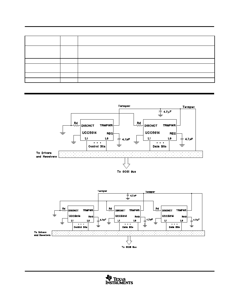
Figure 1. Typical SCSI Bus Configuration Utilizing two UCC5614 Devices
Figure 2. Typical Wide SCSI Bus Configuration Utilizing three UCC5614 Devices
UCC5614
SLUS349A ≠ DECEMBER 1994 ≠ REVISED APRIL 2003
6
www.ti.com
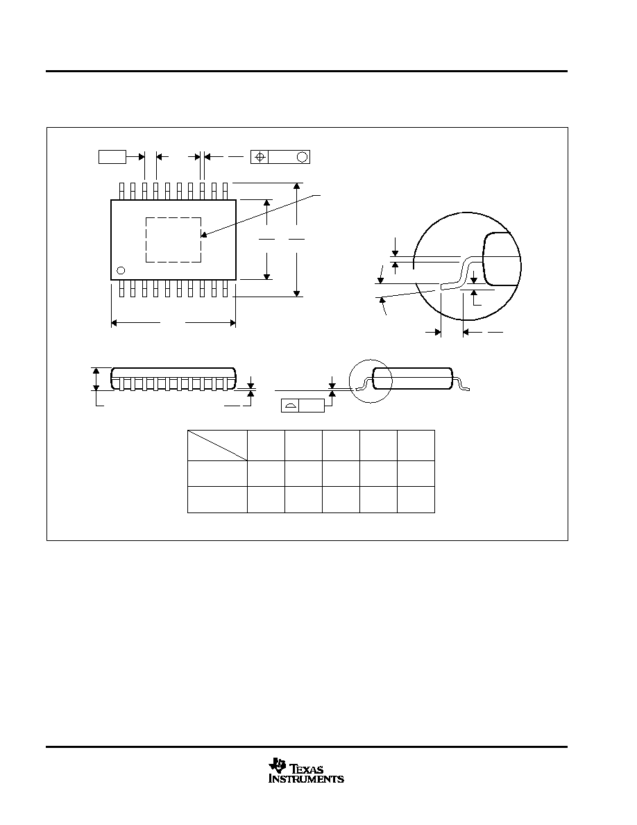
MECHANICAL DATA
PWP (R-PDSO-G**)
PowerPAD
PLASTIC SMALL-OUTLINE
4073225/F 10/98
0,50
0,75
0,25
0,15 NOM
Thermal Pad
(See Note D)
Gage Plane
28
24
7,70
7,90
20
6,40
6,60
9,60
9,80
6,60
6,20
11
0,19
4,50
4,30
10
0,15
20
A
1
0,30
1,20 MAX
16
14
5,10
4,90
PINS **
4,90
5,10
DIM
A MIN
A MAX
0,05
Seating Plane
0,65
0,10
M
0,10
0
∞
≠8
∞
20 PINS SHOWN
NOTES: A. All linear dimensions are in millimeters.
B. This drawing is subject to change without notice.
C. Body dimensions do not include mold flash or protrusions.
D. The package thermal performance may be enhanced by bonding the thermal pad to an external thermal plane.
This pad is electrically and thermally connected to the backside of the die and possibly selected leads.
E. Falls within JEDEC MO-153

IMPORTANT NOTICE
Texas Instruments Incorporated and its subsidiaries (TI) reserve the right to make corrections, modifications,
enhancements, improvements, and other changes to its products and services at any time and to discontinue
any product or service without notice. Customers should obtain the latest relevant information before placing
orders and should verify that such information is current and complete. All products are sold subject to TI's terms
and conditions of sale supplied at the time of order acknowledgment.
TI warrants performance of its hardware products to the specifications applicable at the time of sale in
accordance with TI's standard warranty. Testing and other quality control techniques are used to the extent TI
deems necessary to support this warranty. Except where mandated by government requirements, testing of all
parameters of each product is not necessarily performed.
TI assumes no liability for applications assistance or customer product design. Customers are responsible for
their products and applications using TI components. To minimize the risks associated with customer products
and applications, customers should provide adequate design and operating safeguards.
TI does not warrant or represent that any license, either express or implied, is granted under any TI patent right,
copyright, mask work right, or other TI intellectual property right relating to any combination, machine, or process
in which TI products or services are used. Information published by TI regarding third≠party products or services
does not constitute a license from TI to use such products or services or a warranty or endorsement thereof.
Use of such information may require a license from a third party under the patents or other intellectual property
of the third party, or a license from TI under the patents or other intellectual property of TI.
Reproduction of information in TI data books or data sheets is permissible only if reproduction is without
alteration and is accompanied by all associated warranties, conditions, limitations, and notices. Reproduction
of this information with alteration is an unfair and deceptive business practice. TI is not responsible or liable for
such altered documentation.
Resale of TI products or services with statements different from or beyond the parameters stated by TI for that
product or service voids all express and any implied warranties for the associated TI product or service and
is an unfair and deceptive business practice. TI is not responsible or liable for any such statements.
Mailing Address:
Texas Instruments
Post Office Box 655303
Dallas, Texas 75265
Copyright
2003, Texas Instruments Incorporated