
UCC561
SLUS413B -- MAY 1999 -- REVISED NOVEMBER 2002
LOW-VOLTAGE DIFFERENTIAL SCSI (LVD)
27-LINE REGULATOR SET
FEATURES
D
SCSI SPI--2, SPI--3 and SPI--4 LVD SCSI
27-Line, Low-Voltage Differential Regulator
D
2.7-V to 5.25-V Operation
D
Integrated Regulator Set for LVD SCSI
D
Differential Failsafe Bias
APPLICATIONS
D
Servers
D
Workstations
D
RAID Boxes
DESCRIPTION
The UCC561 low-voltage differential (LVD) regulator
set is designed to provide the correct references
voltages and bias currents for LVD termination resistor
networks (475 9, 121 9, and 475 9). The device also
provides a 1.3-V output for "diff sense" signaling. With
the proper resistor network, the UCC561 solution meets
the common mode bias impedance, differential bias,
and termination impedance requirements of SPI--2
(Ultra2), SPI--3 (Ultra3/Ultra160) and SPI--4 (Ultra320).
The UCC561 is not intended for SPI--5 applications.
This device incorporates into a single monolith, two
sink/source reference voltage regulators, a 1.3-V
buffered output and protection features. The protection
features include thermal shutdown and active
current-limiting circuitry. The UCC561 is offered in
16-pin SOIC (DP) package.
2
DIFSENS
3
TRMPWR
4
PGND
REF 0.75V
7
REG1
6
SOURCE/SINK REGULATOR
REG2
UDG--98093
REF 1.3 V
REF 1.75 V
1.75 V �50 mV
200 mA SOURCE/SINK
1.3 V �100 mV
0.75 V �50 mV
200 mA SOURCE/SINK
2.7 V TO 5.25 V
PRODUCTION DATA information is current as of publication date. Products
conform to specifications per the terms of Texas Instruments standard warranty.
Production processing does not necessarily include testing of all parameters.
Please be aware that an important notice concerning availability, standard warranty, and use in critical applications of Texas Instruments
semiconductor products and disclaimers thereto appears at the end of this data sheet.
www.ti.com
Copyright � 2002, Texas Instruments Incorporated
UCC561
SLUS413B -- MAY 1999 -- REVISED NOVEMBER 2002
www.ti.com
2
This integrated circuit can be damaged by ESD. Texas Instruments recommends that all integrated circuits be handled with appropriate
precautions. Failure to observe proper handling and installation procedures can cause damage.
ESD damage can range from subtle performance degradation to complete device failure. Precision integrated circuits may be more
susceptible to damage because very small parametric changes could cause the device not to meet its published specifications.
ORDERING INFORMATION
PRODUCT
PACKAGE--LEAD
PACKAGE
DESIGNATOR
SPECIFIED
TEMPERATURE
RANGE
ORDERING
NUMBER
TRANSPORT MEDIA,
QUANTITY
UCC561
SOIC--16
DP
0�C to 70�C
UCC561DP
Rail, 70
(1)
For the most current specification and package information, refer to our web site at www.ti.com.
ABSOLUTE MAXIMUM RATINGS
over operating free-air temperature range unless otherwise noted
(1)(2)
UCC561
UNIT
TERMPWR
6
V
Package dissipation
1.2
W
Junction temperature, T
J
--55 to 150
�C
Storage temperature, T
stg
--65 to 150
�C
(1)
Stresses beyond those listed under "absolute maximum ratings" may cause permanent damage to the device. These are stress ratings only, and
functional operation of the device at these or any other conditions beyond those indicated under "recommended operating conditions" is not
implied. Exposure to absolute-maximum-rated conditions for extended periods may affect device reliability.
(2)
Currents are positive into and negative out of the specified terminals.
RECOMMENDED OPERATING CONDITIONS
MIN
NOM
MAX UNIT
V
TERMPWR
, TermPower voltage
2.70
5.25
V
1
2
3
4
5
6
7
8
16
15
14
13
12
11
10
9
NC
TERMPWR
REG2
HSPGND
HSGND
REG1
DIFSENS
NC
NC
NC
NC
HSGND
HSGND
NC
NC
NC
DP PACKAGE
(TOP VIEW)
NC = No connection
UCC561
SLUS413B -- MAY 1999 -- REVISED NOVEMBER 2002
www.ti.com
3
ELECTRICAL CHARACTERISTICS
T
J
= 0�C to 70�C, V
TERMPWR
= 3.3 V unless otherwise noted
(1)
PARAMETER
TEST CONDITIONS
MIN
TYP
MAX
UNIT
TERMPWR Supply Current
TERMPWR supply current
No load
40
mA
TERMPWR voltage
2.70
5.25
V
Regulator
1.75-V regulator
REG1 (�125 mA)
1.70
1.75
1.80
1.3-V regulator
--5 mA � I
DIFSENS
� 50 mA
1.2
1.3
1.4
V
0.75-V regulator
REG2 (�125 mA)
0.70
0.75
0.80
V
1.75-V regulator source current
V
O
= 1.25 V
--200
1.75-V regulator sink current
V
O
= 2.25 V
200
1.75-V regulator source current limit
(1)
--200
--700
mA
1.75-V regulator sink current limit
(1)
200
700
mA
1.3-V regulator source current
V
DIFSENS
= 0 V
--5
--15
1.3-V regulator sink current
V
DIFSENS
= 2.4 V
50
200
mA
0.75-V regulator source current
V
O
= 0.25 V
--200
0.75-V regulator sink current
V
O
= 1.25 V
200
A
0.75-V regulator source current limit
(1)
--200
--700
mA
0.75-V regulator sink current limit
(1)
200
700
(1)
Ensured by design. Not production tested.
TERMINAL FUNCTIONS
TERMINAL
I/O
DESCRIPTION
NAME
NO.
I/O
DESCRIPTION
HSPGND
4
--
Heat sink power ground pin.
HSGND
5, 12, 13
--
Heat sink ground pin which should be attached to the ground plane on a multilayer board or large cop-
per area on a 2 layer board.
REG1
6
O
1.75-V source/sink regulated output voltage pin. The part is internally current limited for both sinking
and sourcing current to prevent damage. For best performance, a 4.7-mF low-ESR capacitor is recom-
mended. Lead lengths should be kept to a minimum.
REG2
3
O
0.75-V source/sink regulated output voltage pin. The part is internally current limited for both sinking
and sourcing current to prevent damage. For best performance, a 4.7-mF low-ESR capacitor is recom-
mended. Lead lengths should be kept to a minimum.
DIFSENS
7
O
1.3-V source/sink regulated output voltage pin. The part is internally current limited to the SCSI SPI--2
through SPI--4 standards for both sinking and sourcing current to prevent damage.
TERMPWR
2
I
Supply voltage pin. The pin should be decoupled with at least a 2.2-mF low-ESR capacitor. For best
performance, a 4.7-mF low--ESR capacitor is recommended. Lead lengths should be kept to a mini-
mum.
UCC561
SLUS413B -- MAY 1999 -- REVISED NOVEMBER 2002
www.ti.com
4
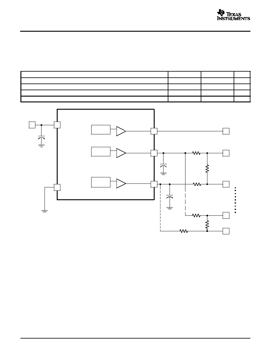
APPLICATION INFORMATION
The resistor stack with the 1.75-V and 0.75-V reference gives the correct differential impedance, bias voltage,
common mode differential impedance, and common mode voltage as show in Table 1.
Table 1. UCC561 Resistor Stack vs. Standard (SPI--2 through SPI--4)
PARAMETER
UCC561
STANDARD
UNITS
Differential Impedance
107.3
100 to 110
W
Differential bias voltage
112.9
100 to 125
mV
Common-mode differential impedance
237
100 to 300
W
Common-mode voltage
1.25
1.2 to 1.3
V
UDG--98096
1.3 V �100 mV
1.75 V �50 mV
200 mA SOURCE/SINK
L1+
L27--
L27+
SOURCE/SINK REGULATOR
REF
1.3V
7
DIFSENS
DIFSENS: SOURCE ONLY FROM TERMPWR
2
TERMPWR
4
PGND
L1--
121 1%
121 1%
6
REF
1.75V
4.7
mF
REG1
3
REG2
SOURCE/SINK REGULATOR
REF
0.75V
200mA SOURCE/SINK
4.7
mF
DIFSENS
475 1%
475 1%
475 1%
475 1%
4.7
mF
TERMPWR
2.7V TO 5.25V
0.75 V �50 mV
Figure 1. Low-Voltage Differential Discrete Resistor Stack

PACKAGING INFORMATION
Orderable Device
Status
(1)
Package
Type
Package
Drawing
Pins Package
Qty
Eco Plan
(2)
Lead/Ball Finish
MSL Peak Temp
(3)
UCC561DP
ACTIVE
SOIC
D
16
40
Green (RoHS &
no Sb/Br)
CU NIPDAU
Level-1-260C-UNLIM
UCC561DPG4
ACTIVE
SOIC
D
16
40
Green (RoHS &
no Sb/Br)
CU NIPDAU
Level-1-260C-UNLIM
UCC561DPTR
ACTIVE
SOIC
D
16
2500 Green (RoHS &
no Sb/Br)
CU NIPDAU
Level-1-260C-UNLIM
UCC561DPTRG4
ACTIVE
SOIC
D
16
2500 Green (RoHS &
no Sb/Br)
CU NIPDAU
Level-1-260C-UNLIM
UCC561TD
OBSOLETE
TO-220
KC
5
TBD
Call TI
Call TI
(1)
The marketing status values are defined as follows:
ACTIVE: Product device recommended for new designs.
LIFEBUY: TI has announced that the device will be discontinued, and a lifetime-buy period is in effect.
NRND: Not recommended for new designs. Device is in production to support existing customers, but TI does not recommend using this part in
a new design.
PREVIEW: Device has been announced but is not in production. Samples may or may not be available.
OBSOLETE: TI has discontinued the production of the device.
(2)
Eco
Plan
-
The
planned
eco-friendly
classification:
Pb-Free
(RoHS)
or
Green
(RoHS
&
no
Sb/Br)
-
please
check
http://www.ti.com/productcontent
for the latest availability information and additional product content details.
TBD: The Pb-Free/Green conversion plan has not been defined.
Pb-Free (RoHS): TI's terms "Lead-Free" or "Pb-Free" mean semiconductor products that are compatible with the current RoHS requirements
for all 6 substances, including the requirement that lead not exceed 0.1% by weight in homogeneous materials. Where designed to be soldered
at high temperatures, TI Pb-Free products are suitable for use in specified lead-free processes.
Green (RoHS & no Sb/Br): TI defines "Green" to mean Pb-Free (RoHS compatible), and free of Bromine (Br) and Antimony (Sb) based flame
retardants (Br or Sb do not exceed 0.1% by weight in homogeneous material)
(3)
MSL, Peak Temp. -- The Moisture Sensitivity Level rating according to the JEDEC industry standard classifications, and peak solder
temperature.
Important Information and Disclaimer:The information provided on this page represents TI's knowledge and belief as of the date that it is
provided. TI bases its knowledge and belief on information provided by third parties, and makes no representation or warranty as to the
accuracy of such information. Efforts are underway to better integrate information from third parties. TI has taken and continues to take
reasonable steps to provide representative and accurate information but may not have conducted destructive testing or chemical analysis on
incoming materials and chemicals. TI and TI suppliers consider certain information to be proprietary, and thus CAS numbers and other limited
information may not be available for release.
In no event shall TI's liability arising out of such information exceed the total purchase price of the TI part(s) at issue in this document sold by TI
to Customer on an annual basis.
PACKAGE OPTION ADDENDUM
www.ti.com
4-Nov-2005
Addendum-Page 1
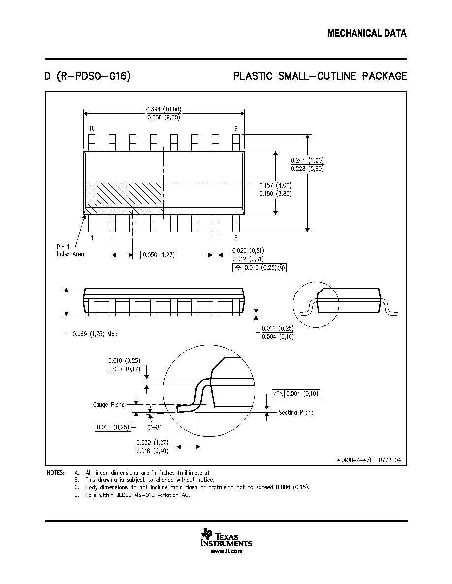
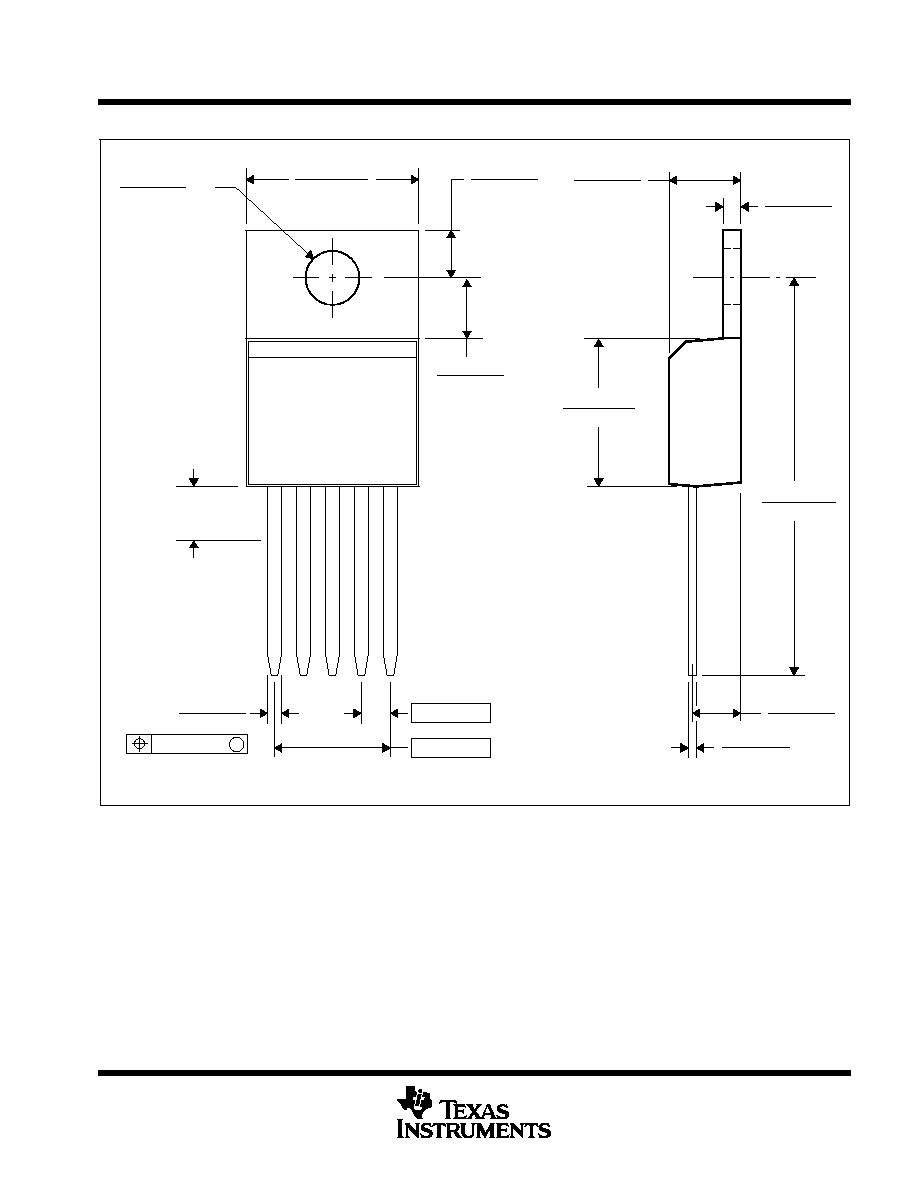
MECHANICAL DATA
MSOT008B � JANUARY 1995 � REVISED SEPTEMBER 2000
1
POST OFFICE BOX 655303
�
DALLAS, TEXAS 75265
KC (R-PSFM-T5)
PLASTIC FLANGE-MOUNT
4040208/E 09/00
0.420 (10,67)
0.185 (4,70)
0.055 (1,40)
0.147 (3,73)
0.340 (8,64)
1.037 (26,34)
0.040 (1,02)
0.030 (0,76)
0.997 (25,32)
0.380 (9,65)
0.330 (8,38)
0.137 (3,48)
0.045 (1,14)
0.175 (4,46)
0.113 (2,87)
0.122 (3,10)
0.025 (0,64)
0.102 (2,59)
0.012 (0,30)
0.103 (2,62)
0.146 (3,71)
0.156 (3,96)
DIA
(see Note C)
0.125 (3,18)
0.067 (1,70)
0.268 (6,81)
5
1
M
0.010 (0,25)
NOTES: A. All linear dimensions are in inches (millimeters).
B. This drawing is subject to change without notice.
C. Lead dimensions are not controlled within this area.
D. All lead dimensions apply before solder dip.
E. The center lead is in electrical contact with the mounting tab.

IMPORTANT NOTICE
Texas Instruments Incorporated and its subsidiaries (TI) reserve the right to make corrections, modifications,
enhancements, improvements, and other changes to its products and services at any time and to discontinue
any product or service without notice. Customers should obtain the latest relevant information before placing
orders and should verify that such information is current and complete. All products are sold subject to TI's terms
and conditions of sale supplied at the time of order acknowledgment.
TI warrants performance of its hardware products to the specifications applicable at the time of sale in
accordance with TI's standard warranty. Testing and other quality control techniques are used to the extent TI
deems necessary to support this warranty. Except where mandated by government requirements, testing of all
parameters of each product is not necessarily performed.
TI assumes no liability for applications assistance or customer product design. Customers are responsible for
their products and applications using TI components. To minimize the risks associated with customer products
and applications, customers should provide adequate design and operating safeguards.
TI does not warrant or represent that any license, either express or implied, is granted under any TI patent right,
copyright, mask work right, or other TI intellectual property right relating to any combination, machine, or process
in which TI products or services are used. Information published by TI regarding third-party products or services
does not constitute a license from TI to use such products or services or a warranty or endorsement thereof.
Use of such information may require a license from a third party under the patents or other intellectual property
of the third party, or a license from TI under the patents or other intellectual property of TI.
Reproduction of information in TI data books or data sheets is permissible only if reproduction is without
alteration and is accompanied by all associated warranties, conditions, limitations, and notices. Reproduction
of this information with alteration is an unfair and deceptive business practice. TI is not responsible or liable for
such altered documentation.
Resale of TI products or services with statements different from or beyond the parameters stated by TI for that
product or service voids all express and any implied warranties for the associated TI product or service and
is an unfair and deceptive business practice. TI is not responsible or liable for any such statements.
Following are URLs where you can obtain information on other Texas Instruments products and application
solutions:
Products
Applications
Amplifiers
amplifier.ti.com
Audio
www.ti.com/audio
Data Converters
dataconverter.ti.com
Automotive
www.ti.com/automotive
DSP
dsp.ti.com
Broadband
www.ti.com/broadband
Interface
interface.ti.com
Digital Control
www.ti.com/digitalcontrol
Logic
logic.ti.com
Military
www.ti.com/military
Power Mgmt
power.ti.com
Optical Networking
www.ti.com/opticalnetwork
Microcontrollers
microcontroller.ti.com
Security
www.ti.com/security
Telephony
www.ti.com/telephony
Video & Imaging
www.ti.com/video
Wireless
www.ti.com/wireless
Mailing Address:
Texas Instruments
Post Office Box 655303 Dallas, Texas 75265
Copyright
2005, Texas Instruments Incorporated