
UCC5628
SLUS302B ≠ DECEMBER 1994 ≠ REVISED APRIL 2003
MULTIMODE SCSI 14 LINE TERMINATOR
1
www.ti.com
FEATURES
D
Auto Selection Single Ended (SE) or Low
Voltage Differential (LVD) Termination
D
Meets SCSI≠1, SCSI≠2, SCSI≠3, SPI, Ultra
(Fast≠20), Ultra2 (SPI≠2 LVD), Ultra3, Ultra160
(SPI≠3) and Ultra320 (SPI≠4) Standards
D
2.7V to 5.25V Operation
D
Differential Failsafe Bias
D
Thermal packaging for low junction
temperature and better MTBF
DESCRIPTION
The UCC5628 Multimode SCSI terminator provides a
smooth transition into the low-voltage differential SCSI
parallel interface (SPI≠2, SPI≠3 and SPI≠4). It
automatically senses the bus, via DIFFB, and switches
the termination to either single ended (SE) or
low-voltage differential (LVD) SCSI, dependent on
which type of devices are connected to the bus. The
UCC5628 can not be used on a high voltage differential
(HVD), EIA485, differential SCSI bus. If the UCC5628
detects a HVD SCSI device, it switches to a
high-impedance state.
BLOCK DIAGRAM
UDG≠98099
REF
1.25V
36
DISCNCT
REG
L1+
L14
L14+
SOURCE/SINK REGULATOR
REF
1.3V
35
DIFFSENS
HPD
SE
34
DIFFB
0.6V
2.15V
52.5
2
52.5
1
110
10
REF
2.7V
SE GND SWITCH
3
TRMPWR
25
GND
4≠9
HS/GND
28≠33
HS/GND
L1
124
52.5
12
52.5
11
110
124
10
µ
A
1.3V
(NOISE LOAD)
MODE
SE
LVD
DISCNCT
ALL SWITCHES
UP
DOWN
OPEN
SE GND SWITCH
56mV
≠ +
+ ≠
≠ +
56mV
56mV
56mV
+ ≠
27
26
LVD
ENABLE
ENABLE
≠15 mA
ISOURCE
≠5 mA
50
µ
A
ISINK
200
µ
A
These devices have limited built-in ESD protection. The leads should be shorted together or the device placed in conductive foam
during storage or handling to prevent electrostatic damage to the MOS gates.
PRODUCTION DATA information is current as of publication date.
Products conform to specifications per the terms of Texas Instruments
standard warranty. Production processing does not necessarily include
testing of all parameters.
Copyright
2003, Texas Instruments Incorporated
UCC5628
SLUS302B ≠ DECEMBER 1994 ≠ REVISED APRIL 2003
2
www.ti.com
DESCRIPTION (CONTINUED)
The Multimode terminator contains all functions required to terminate and auto detect and switch modes for
SPI≠2, SPI≠3 and SPI≠4 bus architectures. Single ended, differential impedances and currents are trimmed for
maximum effectiveness. Fail-safe biasing is provided to insure signal integrity. Device/bus type detection
circuitry is integrated into the terminator to provide automatic switching of termination between single ended
and LVD SCSI and a high impedance for HVD SCSI. The multimode function provides all the performance
analog functions necessary to implement SPI≠2 termination in a single monolithic device.
The UCC5628 is offered in a 48-pin LQFP package for a temperature range of 0
∞
C to 70
∞
C.
ABSOLUTE MAXIMUM RATINGS
over operating free-air temperature range unless otherwise noted
{}
UCC5628
UNIT
TRMPWR voltage
6
V
Signal line voltage
0 to 6
V
Package Dissipation
2
W
Storage temperature, Tstg
≠65 to 150
Operating junction temperature, TJ
≠55 to 150
∞
C
Lead temperature (soldering, 10 sec.)
300
C
Stresses beyond those listed under "absolute maximum ratings" may cause permanent damage to the device. These are stress ratings only,
and functional operation of the device at these or any other conditions beyond those indicated under "recommended operating conditions" is
not implied. Exposure to absolute-maximum-rated conditions for extended periods may affect device reliability. All voltages are with respect
to GND. Currents are positive into and negative out of, the specified terminal.
Currents are positive into, negative out of the specified terminal. Consult Packaging Section of Databook for thermal limitations and
considerations of packages. All voltages are referenced to GND.
RECOMMENDED OPERATING CONDITIONS
MIN
NOM
MAX
UNIT
TRMPWR voltage
2.7
5.25
V
Temperature ranges
0
70
∞
C
ORDERING INFORMATION
T
DISCONNECT STATUS
PACKAGED DEVICE
{
TA
DISCONNECT STATUS
LQFP≠48 (FQP)
0
∞
C to 70
∞
C
UCC5628FQP
The LQFP packages are available taped and reeled. Add TR suffix to device type (e.g. UCC5628FQPTR) to order quantities of 2,500 devices
per reel.

UCC5628
SLUS302B ≠ DECEMBER 1994 ≠ REVISED APRIL 2003
3
www.ti.com
CONNECTION DIAGRAM
12 11 10
9
13
8
7
6
5
4
3
2
1
14
15
16
17
18
19
20
21
22
23
24
25 26 27 28
29 30 31 32
33 34 35 36
48
47
46
45
44
43
42
41
40
39
38
37
TRMPWR
HS/GND
HS/GND
HS/GND
L1≠
L1+
REG
HS/GND
HS/GND
HS/GND
L9≠
L10+
L9+
DIFFSENS
DISCNCT
HS/GND
DIFFB
HS/GND
HS/GND
GND
SE
LVD
HS/GND
HS/GND
HS/GND
L4+
L3≠
L3+
L2≠
L2+
L4≠
L5+
L6+
L5≠
L7+
L6≠
L7≠
L11+
L11≠
L10≠
L12≠
L13+
L12+
L14+
L14≠
L13≠
L8≠
L8+
ELECTRICAL CHARACTERISTICS
T
A
= T
J
= 0
∞
C to 70
∞
C, TRMPWR = 3.3 V, (unless otherwise noted)
PARAMETER
TEST CONDITIONS
MIN
TYP
MAX
UNITS
TRMPWR Supply Current Section
LVD mode
20
25
mA
TRMPWR supply current
SE mode
1.6
10.0
mA
TRMPWR su
ly current
Disabled terminator
250
400
µ
A
Regulator Section
1.25-V regulator
LVD mode
1.15
1.25
1.35
V
1.25-V regulator source current
VREG = 0 V
≠375
≠700
≠1000
mA
1.25-V regulator sink current
VREG = 3.3 V
170
300
700
mA
1.3-V regulator
Diff sense
1.2
1.3
1.4
V
1.3-V regulator source current
VREG = 0 V
≠15
≠5
mA
1.3-V regulator sink current
VREG = 3.3 V
50
200
µ
A
2.7-V regulator
SE mode
2.5
2.7
3.0
V
2.7-V regulator source current
VREG = 0 V
≠375
≠700
≠1000
mA
2.7-V regulator sink current
VREG = 3.3 V
170
300
700
mA
Differential Termination Section
Differential impedance
100
105
110
Common mode impedence
(2)
110
150
165
Differential bias voltage
100
125
mV
Common mode bias
1.15
1.25
1.35
V
Output capacitance
Single Ended Measurement to Ground (Note 1)
3
pF
UCC5628
SLUS302B ≠ DECEMBER 1994 ≠ REVISED APRIL 2003
4
www.ti.com
ELECTRICAL CHARACTERISTICS
T
A
= T
J
= 0
∞
C to 70
∞
C, TRMPWR = 3.3 V, (unless otherwise noted)
PARAMETER
TEST CONDITIONS
MIN
TYP
MAX
UNITS
Single Ended Termination Section
Impedance
(3)
Z
+
VL
X
*
0.2 V
IL
X
102.3
110.0
117.7
W
Termination current
Signal level 0.2 V,
all lines low
≠21.0
≠24.0
≠25.4
mA
Termination current
Signal level 0.5 V
≠18.0
≠22.4
mA
Output leakage
400
nA
Output capacitance
Single ended measurement to ground (1)
3
pF
Single ended GND impedance
I = 10 mA
20
60
W
Disconnect and Diff Buffer Input Section
DISCNCT threshold
0.8
2.0
V
DISCNCT input current
10
30
mA
Diff buffer single ended to LVD threshold
0.5
0.7
V
Diff buffer LVD to HPD threshold
1.9
2.4
V
DIFFB input current
≠10
10
mA
Status Bits (SE, LVD) Output Section
ISOURCE
VLOAD = 2.4 V
≠4
≠6
mA
ISINK
VLOAD = 0.4 V
2
5
mA
NOTES:
1. Ensured by design. Not production tested.
2.
Z
CM
+
1.2 V
I
VCM
)
0.6 V
*
I
VCM
*
0.6 V , where VCM=voltage measured with L+ tied to L≠ and zero current applied.
3. VLX= Output voltage for each terminator minus output pin (L1≠ through L14≠) with each pin unloaded.
ILX = Output current for each terminator minus output pin (L1≠ through L14≠) with the minus output pin forced to 0.2 V.
TERMINAL FUNCTIONS
TERMINAL
I/O
DESCRIPTION
NAME
NO.
I/O
DESCRIPTION
DIFFB
34
I
DIFFSENS filter pin should be connected to a 4.7-
µ
F capacitor and a 50-k
resistor.
DIFFSENS
35
O
The SCSI bus Diff sense line to detect what types of devices are connected to the SCSI bus.
DISCNCT
36
I
Disconnect pin shuts down the terminator when it is not at the end of the bus. The disconnect pin
high enables the terminator.
GND
25
Analog ground.
HS/GND
Heatsink ground pins must be connected to a large ground area.
LINEn≠
Signal line active line for single ended or negative line in differential applications for the SCSI bus.
LINEn+
Ground line for single ended or positive line for differential applications for the SCSI bus.
LVD
27
O
TTL compatible status bit indicating that the device has detected the bus in LVD mode. This output is
not valid in disconnect mode.
REG
10
O
Regulator bypass pin, must be connected to a 4.7-
µ
F capacitor.
SE
26
O
TTL compatible status bit indicating that the device has detected the bus in single ended mode. This
output is not valid in disconnect mode.
TRMPWR
3
VIN 2.7-V to 5.25-V supply, bypass near the terminators with a 4.7-
µ
F capacitor to ground.

UCC5628
SLUS302B ≠ DECEMBER 1994 ≠ REVISED APRIL 2003
5
www.ti.com
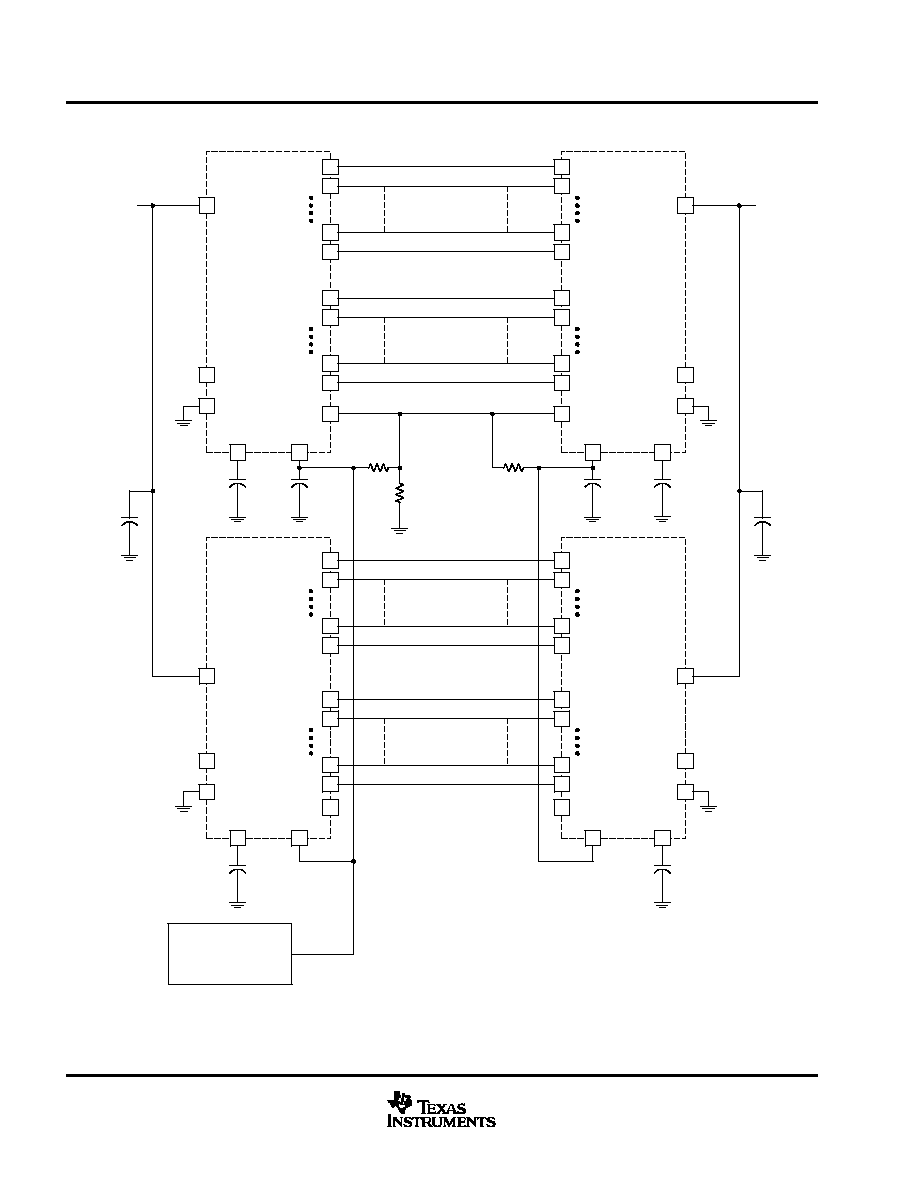
APPLICATION INFORMATION
The UCC5628 is a multimode active terminator with selectable single ended (SE) and low voltage differential
(LVD) SCSI termination integrated into a monolithic component. Mode selection is accomplished with the diff
sense signal.
The diff sense signal is a three level signal, which is driven at each end of the bus by one active terminator. A
LVD or multimode terminator drives the diff sense line to 1.3 V. If diff sense is at 1.3 V, then bus is in LVD mode.
If a single ended SCSI device is plugged into the bus, the diff sense line is shorted to ground. With diff sense
shorted to ground, the terminator changes to single ended mode to accommodate the SE device. If a HVD
device is plugged in to the bus, the diff sense line is pulled high and the terminator shuts down.
The diff sense line is driven and monitored by the terminator through a 50-Hz noise filter for SPI≠2 and a 100-ms
to 300-ms filter for SPI≠3 and SPI≠4 at the DIFFB input pin. A set of comparators, that allow for ground shifts,
determine the bus status as follows. Any diff sense signal below 0.5 V is single ended, between 0.7 V and 1.9
V is LVD and above 2.4 V is HVD.
In the single ended mode, a multimode terminator has a 110-
terminating resistor connected to a 2.7-V
termination voltage regulator. The 2.7-V regulator is used on all unitrode terminators designed for 3.3-V
systems. This requires the terminator to operate in specification down to 2.7-V TRMPWR voltage to allow for
the 3.3-V supply tolerance, an unidirectional fusing device and cable drop. At each L+ pin, a ground driver drives
the pin to ground, while in single ended mode. The ground driver is specially designed so it will not effect the
capacitive balance of the bus when the device is in LVD or disconnect mode. The device requirements call for
1.5-pF balance on the lines of a differential pair. The terminator capacitance has to be a small part of the
capacitance imbalance.
Layout is very critical for Ultra2, Ultra3, Ultra160 and Ultra320 systems. Multilayer boards need to adhere to the
120-
impedance standard, including connector and feed-through. This is normally done on the outer layers
with 4-mil etch and 4-mil spacing between the runs within a pair, and a minimum of 8-mil spacing to the next
pair. This spacing between the pairs reduces potential crosstalk. Beware of feed-throughs and each
through-hole connection adds a lot of capacitance. Standard power and ground plane spacing yields about 1
pF to each plane. Each feed-through will add about 2.5 pF to 3.5 pF. Enlarging the clearance holes on both power
and ground planes can reduce the capacitance and opening up the power and ground planes under the
connector can reduce the capacitance for through-hole connector applications. Microstrip technology is
normally too low of impedance and should not be used. It is designed for 50
rather than 120-
differential
systems.
Capacitance balance is critical for Ultra2, Ultra3, Ultra160 and Ultra320. The balance capacitance standard is
0.5 pF per line with the balance between pairs of 2 pF. The components are designed with very tight balance,
typically 0.1 pF between pins in a pair and 0.3 pF between pairs. Layout balance is critical, feed-throughs and
etch length must be balanced, preferably no feed-throughs would be used. Capacitance for devices should be
measured in the typical application, material and components above and below the circuit board effect the
capacitance.
Multimode terminators need to consider power dissipation; the UCC5628 is offered in a power package with
heat sink ground pins. These heat-sink ground pins are directly connected to the die mount paddle under the
die and conduct heat from the die to reduce the junction temperature. These pins need to be connected to etch
area or a feed-through per pin connecting to the ground plane layer on a multilayer board.
In 3.3-V TRMPWR systems, the UCC3912 should be used to replace the fuse and diode. This reduces the
voltage drop, allowing for cable drop to the far end terminator. 3.3-V battery systems normally have a 10%
tolerance. The UCC3912 is 150-mV drop under LVD loads, allowing 150-mV drop in the cable system. All
Unitrode LVD and multimode terminators are designed for 3.3-V systems, operating down to 2.7 V.
UCC5628
SLUS302B ≠ DECEMBER 1994 ≠ REVISED APRIL 2003
6
www.ti.com
APPLICATION INFORMATION
UDG≠98100
REG
TRMPWR
DISCNCT
TRMPWR
DIFFB
REG
DIFFB
TRMPWR
TRMPWR
4.7
µ
F
4.7
µ
F*
4.7
µ
F
4.7
µ
F*
3
36
35
10
34
35
34
10
3
DISCNCT 36
DIFFSENS
DIFFSENS
REG
TRMPWR
DISCNCT
DIFFB
4.7
µ
F
3
36
10
34
DATA LINES (15)
TRMPWR
REG
DIFFB
4.7
µ
F
34
10
DATA LINES (15)
3
DISCNCT 36
4.7
µ
F
50 k
220 k
50 k
SCSI CONTROLLER
DIFFSENS
4.7
µ
F
CONTROL LINES
9 BITS
L1+
L1≠
L9+
L9≠
L1+
L1≠
L9+
L9≠
4 BITS OF THE HIGH BYTE
L10+
L10≠
L13+
L13≠
L10+
L10≠
L13+
L13≠
L1+
L1≠
L9+
L9≠
L1+
L1≠
L9+
L9≠
LOW BYTE 8 BITS
PLUS PARITY
L10+
L10≠
L14+
L14≠
L10+
L10≠
L14+
L14≠
HIGH BYTE 4 BITS
PLUS PARITY
35
35 NC
NC
GND
25
GND
25
25
GND
25
GND
NOTE: A 220-k
resistor is added to ground to insure the transceivers will come up in single-ended mode when no terminator is enabled. The
controller DIFFSENS ties to the DIFFB pin on the terminators, only one RC network should be on a device.
NOTE: * For SPI≠2 systems a 20-k
resistor and 0.1-
µ
F capacitor is used. For SPI≠3 and SPI≠4 systems a 50-k
resistor and 4.7-
µ
F capacitor
is used.
UCC5628
SLUS302B ≠ DECEMBER 1994 ≠ REVISED APRIL 2003
7
www.ti.com
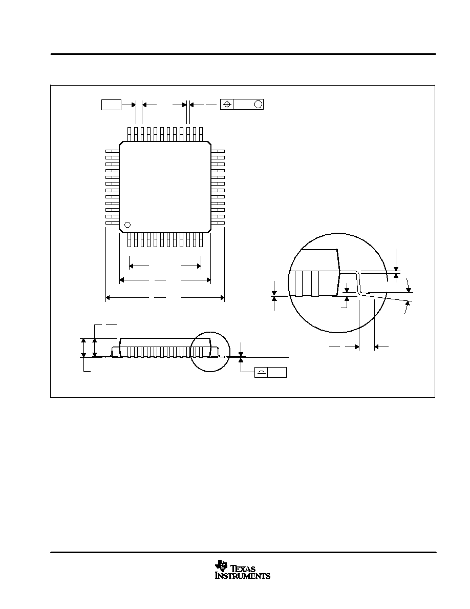
MECHANICAL DATA
PT (S-PQFP-G48)
PLASTIC QUAD FLATPACK
4040052/C 11/96
0,13 NOM
0,17
0,27
25
24
SQ
12
13
36
37
6,80
7,20
1
48
5,50 TYP
0,25
0,45
0,75
0,05 MIN
SQ
9,20
8,80
1,35
1,45
1,60 MAX
Gage Plane
Seating Plane
0,10
0
∞
≠7
∞
0,50
M
0,08
NOTES: A. All linear dimensions are in millimeters.
B. This drawing is subject to change without notice.
C. Falls within JEDEC MS-026
D. This may also be a thermally enhanced plastic package with leads conected to the die pads.

IMPORTANT NOTICE
Texas Instruments Incorporated and its subsidiaries (TI) reserve the right to make corrections, modifications,
enhancements, improvements, and other changes to its products and services at any time and to discontinue
any product or service without notice. Customers should obtain the latest relevant information before placing
orders and should verify that such information is current and complete. All products are sold subject to TI's terms
and conditions of sale supplied at the time of order acknowledgment.
TI warrants performance of its hardware products to the specifications applicable at the time of sale in
accordance with TI's standard warranty. Testing and other quality control techniques are used to the extent TI
deems necessary to support this warranty. Except where mandated by government requirements, testing of all
parameters of each product is not necessarily performed.
TI assumes no liability for applications assistance or customer product design. Customers are responsible for
their products and applications using TI components. To minimize the risks associated with customer products
and applications, customers should provide adequate design and operating safeguards.
TI does not warrant or represent that any license, either express or implied, is granted under any TI patent right,
copyright, mask work right, or other TI intellectual property right relating to any combination, machine, or process
in which TI products or services are used. Information published by TI regarding third≠party products or services
does not constitute a license from TI to use such products or services or a warranty or endorsement thereof.
Use of such information may require a license from a third party under the patents or other intellectual property
of the third party, or a license from TI under the patents or other intellectual property of TI.
Reproduction of information in TI data books or data sheets is permissible only if reproduction is without
alteration and is accompanied by all associated warranties, conditions, limitations, and notices. Reproduction
of this information with alteration is an unfair and deceptive business practice. TI is not responsible or liable for
such altered documentation.
Resale of TI products or services with statements different from or beyond the parameters stated by TI for that
product or service voids all express and any implied warranties for the associated TI product or service and
is an unfair and deceptive business practice. TI is not responsible or liable for any such statements.
Mailing Address:
Texas Instruments
Post Office Box 655303
Dallas, Texas 75265
Copyright
2003, Texas Instruments Incorporated