 | –≠–ª–µ–∫—Ç—Ä–æ–Ω–Ω—ã–π –∫–æ–º–ø–æ–Ω–µ–Ω—Ç: UCC5631A | –°–∫–∞—á–∞—Ç—å:  PDF PDF  ZIP ZIP |

UCC5631A
DESCRIPTION
The UCC5631A Multimode SCSI Terminator provides a smooth transition
into the next generation of the SCSI Parallel Interface (SPI-2). It automati-
cally senses the bus, via DIFFB, and switches the termination to either sin-
gle ended (SE) or low voltage differential (LVD) SCSI, dependent on which
type of devices are connected to the bus. The UCC5631A can not be used
on a HVD, EIA485, differential SCSI bus. If the UCC5631A detects a HVD
SCSI device, it switches to a high impedance state.
The Multimode terminator contains all functions required to terminate and
auto detect and switch modes for SPI-2 bus architectures. Single Ended
and Differential impedances and currents are trimmed for maximum effec-
tiveness. Fail Safe biasing is provided to insure signal integrity. Device/Bus
type detection circuitry is integrated into the terminator to provide automatic
switching of termination between single ended and LVD SCSI and a high
impedance for HVD SCSI. The multimode function provides all the perfor-
mance analog functions necessary to implement SPI-2 termination in a sin-
gle monolithic device.
The UCC5631A is offered in a 36 pin SSOP package, as well as a 48 pin
LQFP package for a temperature range of 0∞C to 70∞C.
Multimode SCSI 9 Line Terminator
FEATURES
∑
Auto Selection Single Ended (SE) or
Low Voltage Differential (LVD)
Termination
∑
Meets SCSI-1, SCSI-2, SCSI-3, SPI,
Ultra (Fast-20), Ultra2 (SPI-2 LVD)
and Ultra3 Standards
∑
2.7V to 5.25V Operation
∑
Differential Failsafe Bias
∑
Thermal packaging for low junction
temperature and better MTBF
∑
Master/Slave Input
∑
Supports Active Negation
∑
3pF Channel Capacitance
∑
Reversed Disconnect Polarity
SLUS443 - OCTOBER 1999
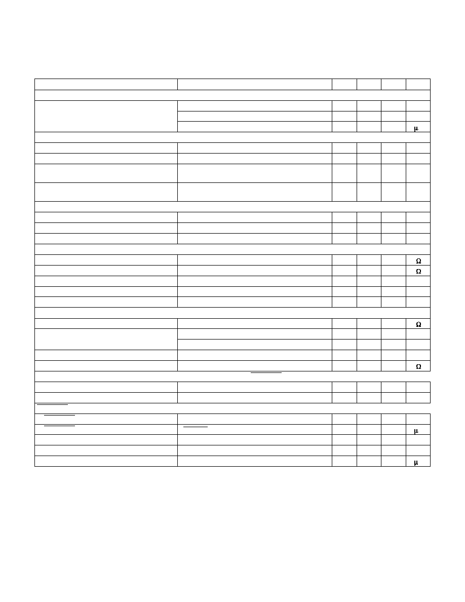
LVD REF 1.25V
17
DISCNCT
REG
L1+
L9≠
L9+
SOURCE/SINK REGULATOR
REF 1.3V
20
DIFSENS
≠15mA
I
SOURCE
≠5mA
50
µ
A
I
SINK
200
µ
A
HIPD
LVD
SE
21
DIFFB
0.6V
2.15V
52.5
32
52.5
31
110
1
SE REF 2.7V
SE GND SWITCH
36
TRMPWR
18
GND
9
L1≠
124
52.5
5
52.5
4
110
124
10
µ
A
1.3V
(NOISE LOAD)
SE GND SWITCH
56mV
≠ +
+ ≠
≠ +
56mV
56mV
56mV
+ ≠
MODE
ALL
SWITCHES
SE
LVD
HIPD
DISCNCT
UP
DOWN
OPEN
OPEN
35
HIPD
34
LVD
33
SE
19
ENABLE
SWITCHES
MSTR/SLV
PATENTED CIRCUIT DESIGN
8
HS/GND
10
27
26
28
BLOCK DIAGRAM
UDG-99165
Note: Indicated pinout is for 36 pin SSOP package.

2
UCC5631A
ABSOLUTE MAXIMUM RATINGS
TRMPWR Voltage . . . . . . . . . . . . . . . . . . . . . . . . . . . . . . . . . 6V
Signal Line Voltage . . . . . . . . . . . . . . . . . . . . . 0V to TRMPWR
Package Power Dissipation . . . . . . . . . . . . . . . . . . . . . . . . . 2W
Storage Temperature . . . . . . . . . . . . . . . . . . . ≠65∞C to +150∞C
Junction Temperature . . . . . . . . . . . . . . . . . . . ≠55∞C to +150∞C
Lead Temperature (Soldering, 10sec.) . . . . . . . . . . . . . +300∞C
All voltages are with respect to pin 18. Currents are positive
into, negative out of the specified terminal. Consult Packaging
Section of the Databook for thermal limitations and consider-
ations of packages.
RECOMMENDED OPERATING CONDITIONS
TRMPWR Voltage . . . . . . . . . . . . . . . . . . . . . . . . 2.7V to 5.25V
L3+
HS/GND
L9≠
L9+
L8≠
TRMPWR
N/C
N/C
HS/GND
L2≠
HS/GND
L1+
L1≠
L2+
REG
HS/GND
L3≠
L8+
HS/GND
HS/GND
L4+
L4≠
14
13
12
11
10
9
8
7
6
5
4
3
2
1
23
24
25
26
27
28
29
30
31
32
33
34
35
36
18
17
16
15
DIFF B
MSTR/SLV
DIFSENS
19
20
21
22
L5+
L5≠
DISCNCT
GND
L7≠
L7+
L6≠
L6+
HIPD
LVD
SE
CONNECTION DIAGRAM
48
47
46
45
1
44
43
42
41
40
39
38
37
2
3
4
5
6
7
8
9
10
11
12
13
14
15
16
17
18
19
20
21
22
23
24
36
35
34
33
32
31
30
29
28
27
26
25
NC
L3+
L3≠
L4+
L4≠
HS/GND
GND
DISCNCT
L5+
HS/GND
HS/GND
L1+
L1≠
L2+
L2≠
NC
HS/GND
REG
NC
NC
TERMPWR
NC
LVD
HIPD
L8+
L8≠
L9+
L9≠
HS/GND
N/C
DIFFB
DIFSENS
L6+
HS/GND
L7+
L6≠
L7≠
HS/GND
HS/GND
HS/GND
L5≠
HS/GND
HS/GND
SE
HS/GND
HS/GND
HS/GND
MSTR/SLV
LQFP-48 (Top View)
FQP Package
QSOP-36 (Top View)
MWP Package
3
UCC5631A
ELECTRICAL CHARACTERISTICS
Unless otherwise stated, these specifications apply for T
A
= T
J
= 0∞C to 70∞C,
TRMPWR = 2.7V to 5.25V.
PARAMETER
TEST CONDITIONS
MIN
TYP
MAX
UNITS
TRMPWR Supply Current Section
TRMPWR Supply Current
LVD Mode (No Load)
13
20
mA
SE Mode (No Load)
1.6
10
mA
Disabled
250
400
A
Regulator Section
REG Output Voltage (LVD Mode)
0.5V
V
CM
2.0V (Note1)
1.15
1.25
1.35
V
REG Output Voltage (SE Mode)
0V
V
L≠
4.2V (Note2)
2.5
2.7
3.0
V
REG Short-Circuit Source Current
(LVD and SE Modes)
V
REG
= 0V
≠800
≠420
≠225
mA
REG Short-Circuit Sink Current
(LVD and SE Modes)
V
REG
= 3.0V
100
180
800
mA
DIFSENS Output Section
Output Voltage
≠5mA
I
DIFSENS
50
µ
A
1.2
1.3
1.4
V
Short-Circuit Source Current
V
DIFSENS
= 0V
≠15
≠8
≠5
mA
Short-Circuit Sink Current
V
DIFSENS
= 2.75V
50
80
200
µ
A
Differential Termination Section (Applies to each line pair, 1-9, in LVD mode)
Differential Impedance
100
105
110
Common Mode Impedance
L+ and L≠ shorted together. (Note 3)
110
140
165
Differential Bias Voltage
100
125
mV
Common Mode Bias Voltage
L+ and L≠ shorted together.
1.15
1.25
1.35
V
Output Capacitance
Single ended measurement to ground. (Note 4)
3
pF
Single Ended Termination Section (Applies to each line pair, 1-9, in SE mode)
Impedance
(Note 5)
102.3
110
117.7
Termination Current
Signal Level 0.2V
≠25.4
≠21
mA
Signal Level 0.5V
≠22.4
≠18
mA
Output Capacitance
Single ended measurement to ground. (Note 4)
3
pF
Single Ended GND Switch Impedance
I= 10mA
20
60
Disconnected Termination Section (Applies to each line pair, 1-9, in DISCNCT or HIPD mode)
Output Leakage
400
nA
Output Capacitance
Single ended measurement to ground. (Note 4)
3
pF
DISCNCT and DIFFB Input Section
DISCNCT Threshold
0.8
2.0
V
DISCNCT Input Current
V
DISCNCT
= 0V
≠30
≠10
≠ 3
A
DIFFB Single Ended to LVD Threshold
0.5
0.7
V
DIFFB LVD to HIPD Threshold
1.9
2.4
V
DIFFB Input Current
0V
V
DIFFB
2.75V
≠1
1
A
4
UCC5631A
PIN DESCRIPTIONS
DIFFB:
Input pin for the comparators that select SE,
LVD, or HIPD modes of operation. This pin should be de-
coupled with a 0.1 F capacitor to ground and then cou-
pled to the DIFSENS pin through a 20k resistor.
DIFSENS: Connects to the Diff Sense line of the SCSI
bus. The bus mode is controlled by the voltage level on
this pin.
DISCNCT: Input pin used to shut down the terminator if
the terminator is not connected at the end of the bus.
Connect this pin to ground to disable the terminator or
open pin to activate the terminator.
HIPD: TTL compatible status bit. This output pin is high
when a high voltage differential device is detected on the
bus.
HS/GND: Heat sink ground pins. These should be con-
nected to large area PC board traces to increase the
power dissipation capability.
GND: Power Supply return.
L1≠ thru L9≠: Termination lines. These are the active
lines in SE mode and are the negative lines for LVD
mode. In HIPD mode, these lines are high impedance.
L1+ thru L9+: Termination lines. These lines switch to
ground in SE mode and are the positive lines for LVD
mode. In HIPD mode, these lines are high impedance.
MSTR/SLV: If the terminator is enabled, this input pin en-
ables / disables the DIFSENS driver, when connected to
TRMPWR or ground respectively. When the terminator is
disabled, the DIFSENS driver is off, independent of this
input.
LVD: TTL compatible status bit. This output pin is high
when the SCSI bus is in LVD mode.
REG:
Regulator output bypass pin. This pin must be
connected to a 4.7 F capacitor to ground.
SE: TTL compatible status bit. This output pin is high
when the SCSI bus is in SE mode.
TRMPWR: 2.7V to 5.25V power input pin.
ELECTRICAL CHARACTERISTICS
Unless otherwise stated, these specifications apply for T
A
= T
J
= 0∞C to 70∞C,
TRMPWR = 2.7V to 5.25V.
PARAMETER
TEST CONDITIONS
MIN
TYP
MAX
UNITS
Master/Slave (MSTR/SLV) Input Section
MSTR/SLV Threshold
V
TRMPWR
= 2.7V
0.8
1.9
V
V
TRMPWR
= 3.3V
1
2.4
V
V
TRMPWR
= 5.25V
1.5
3.7
V
MSTR/SLV Input Current
≠1
1
A
Status Bits (SE, LVD, HIPD) Output Section
I
SOURCE
V
LOAD
= 2.4V
≠8.7
≠4
mA
I
SINK
V
LOAD
= 0.5V
3
6
mA
V
LOAD
= 0.4V
2
5
mA
Note 1: V
CM
is applied to all L+ and L≠ lines simultaneously.
Note 2: V
L≠
is applied to all L≠ lines simultaneously.
Note 3:
(
)
(
)
(
)
Z
V
V
I
I
CM
at V
V
at V
V
CM
CM
=
-
-
=
=
2 0
0 5
2
0 5
.
.
.
;
Note 4: Guaranteed by design. Not 100% tested in production.
Note 5:
( )
( )
Z
V
V
I
L X
L X
=
-
0 2
.
; where
VL
(X)
= Output voltage for each terminator minus output pin (L1≠ through L9≠) with each pin unloaded.
IL
(X )
= Output current for each terminator minus output pin (L1≠ through L9≠) with the minus output pin forced to 0.2V.

5
UCC5631A
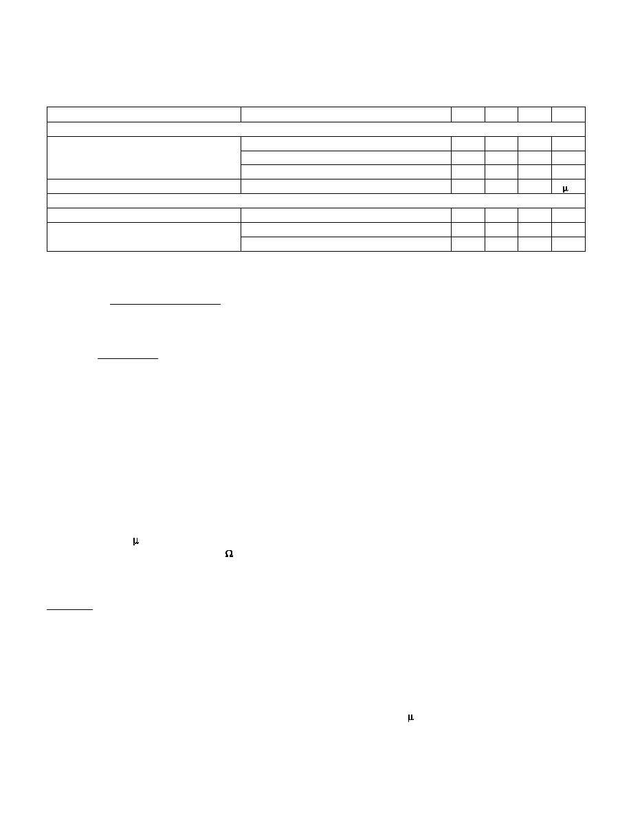
REG
TERMPWR
DISCNCT
TERMPWR
DIFFB
REG
DIFF B
TERMPWR
TERMPWR
4.7
µ
F
.
4.7
µ
F
.
0.1
µ
F
.
4.7
µ
F
0.1
µ
F
.
36
17
20
1
21
20
21
1
CONTROL LINES
36
DISCNCT 17
CONTROL LINES
DIFSENS
DIFSENS
REG
TERMPWR
DISCNCT
DIFF B
4.7
µ
F
.
36
17
1
21
DATA LINES (9)
REG
TERMPWR
DIFFB
4.7
µ
F
.
36
19
1
21
DATA LINES (9)
TERMPWR
REG
DIFFB
4.7
µ
F
21
1
DATA LINES (9)
36
DISCNCT 17
TERMPWR
REG
DIFFB
4.7
µ
F
21
1
DATA LINES (9)
36
DISCNCT 17
4.7
µ
F
.
MSTR/SLV
19
19
MSTR/SLV
19
MSTR/SLV
19
MSTR/SLV
MSTR/SLV
19
DISCNCT
17
MSTR/SLV
20k
20k
APPLICATION INFORMATION
Figure 2. Application diagram.
UDG-99166
All SCSI buses require a termination network at each
end to function properly. Specific termination require-
ments differ, depending on which types of SCSI devices
are present on the bus.
The UCC5631A is used in multi-mode active termination
applications, where single ended (SE) and low voltage
differential (LVD) devices might coexist. The UCC5631A
has both SE and LVD termination networks integrated
into a single monolithic component. The correct termina-
tion network is automatically determined by the SCSI bus
"DIFSENS" signal.
The SCSI bus DIFSENS signal line is used to identify
which types of SCSI devices are present on the bus. On
power-up, the UCC5631A DIFSENS drivers will try to de-
liver 1.3V to the DIFSENS line. If only LVD devices are
present, the DIFSENS line will be successfully driven to
1.3V and the terminators will configure for LVD operation.
If any single ended devices are present, they will present
a short to ground on the DIFSENS line, signaling the
UCC5631A(s) to configure into the SE mode, accommo-
dating the SE devices. Or, if any high voltage differential
(HVD) devices are present, the DIFSENS line is pulled
high and the terminator will enter a high impedance
state, effectively disconnecting from the bus.

6
UCC5631A
UNITRODE CORPORATION
7 CONTINENTAL BLVD. ∑ MERRIMACK, NH 03054
TEL. (603) 424-2410 ∑ FAX (603) 424-3460
The DIFSENS line is monitored by each terminator
through a 50Hz noise filter at the DIFFB input pin. A set
of comparators detect and select the appropriate termi-
nation for the bus as follows. If the DIFSENS signal is be-
low 0.5V, the termination network is SE. Between 0.7V
and 1.9V, the termination network switches to LVD, and
above 2.4V is HVD, causing the terminators to discon-
nect from the bus. The thresholds accommodate differ-
ences in ground potential that can occur with long lines.
Three UCC5631A multi-mode parts are required at each
end of the bus to terminate 27 (18 data, plus 9 control)
lines. Each part includes a DIFSENS driver, but only one
is necessary to drive the line. A MSTR/SLV input pin is
provided to disable the other two. The "master" part must
have its' MSTR/SLV pin connected to TRMPWR and the
two "slave" parts must have the MSTR/SLV inputs
grounded. Only the "master" is connected directly to the
SCSI bus DIFSENS line. The DIFFB inputs on all three
parts are connected together, allowing them to share the
same 50Hz noise filter. This multi-mode terminator oper-
ates in full specification down to 2.7V TRMPWR voltage.
This accommodates 3.3V systems, with allowance for the
3.3V supply tolerance (+/- 10%), a unidirectional fusing
device and cable drop. In 3.3V TRMPWR systems, the
UCC3912 is recommended in place of the fuse and di-
ode. The UCC3912's lower voltage drop allows additional
margin over the fuse and diode, for the far end termina-
tor.
Layout is critical for Ultra2 and Ultra3 systems. The SPI-2
standard for capacitance loading is 10pF maximum from
each positive and negative signal line to ground, and a
maximum of 5pF between the positive and negative sig-
nal lines of each pair is allowed. These maximum capaci-
tances apply to differential bus termination circuitry that
is not part of a SCSI device, (e.g. a cable terminator). If
the termination circuitry is included as part of a SCSI de-
vice, (e.g., a host adaptor, disk or tape drive), then the
corresponding requirements are 30pF maximum from
each positive and negative signal line to ground and
15pF maximum between the positive and negative signal
lines of each pair.
The SPI-2 standard for capacitance balance of each pair
and balance between pairs is more stringent. The stan-
dard is 0.75pF maximum difference from the positive and
negative signal lines of each pair to ground. An additional
requirement is a maximum difference of 2pF when com-
paring pair to pair. These requirements apply to differen-
tial bus termination circuitry that is not part of a SCSI
device. If the termination circuitry is included as part of a
device, then the corresponding balance requirements are
2.25pF maximum difference within a pair, and 3pF from
pair to pair.
Feed-throughs,
through-hole
connections,
and
etch
lengths
need
to
be
carefully
balanced. Standard
multi-layer power and ground plane spacing add about
1pF to each plane. Each feed-through will add about
2.5pF to 3.5pF. Enlarging the clearance holes on both
power and ground planes will reduce the capacitance.
Similarly, opening up the power and ground planes under
the
connector
will
reduce
the
capacitance
for
through-hole connector applications. Capacitance
will
also be affected by components, in close proximity,
above and below the circuit board.
Unitrode multi-mode terminators are designed with very
tight balance, typically 0.1pF between pins in a pair and
0.3pF between pairs. At each L+ pin, a ground driver
drives the pin to ground, while in single ended mode. The
ground driver is specially designed to not effect the ca-
pacitive balance of the bus when the device is in LVD or
disconnect mode.
Multi-layer boards need to adhere to the 120
imped-
ance standard, including the connectors and feed-
throughs. This is normally done on the outer layers with
4 mil etch and 4 mil spacing between runs within a pair,
and a minimum of 8 mil spacing to the adjacent pairs to
reduce crosstalk. Microstrip technology is normally too
low of impedance and should not be used. It is designed
for 50
rather than 120
differential systems. Careful
consideration must be given to the issue of heat man-
agement. A multi-mode terminator, operating in SE
mode, will dissipate as much as 130mW of instanta-
neous power per active line with TRMPWR = 5.25V. The
UCC5631A is offered in a 36 pin SSOP and a 48 lead
LFQP. Both packages include heat sink ground pins.
These heat sink/ground pins are directly connected to
the die mount paddle under the die and conduct heat
from the die to reduce the junction temperature. All of the
HS/GND pins need to be connected to etch area or a
feed-through per pin connecting to the ground plane
layer on a multi-layer board.
APPLICATION INFORMATION (cont.)