UCC5640
SLUS314B - JANUARY 2000 - REVISED MARCH 2002
FEATURES
∑ First LVD only Active Terminator
∑ Meets SCSI SPI-2 Ultra2 (Fast-40)
SPI-3 Ultra3 / Ultra160 (Fast-80) and
SPI-4 (Fast-160) Ultra320 Standards
∑ 2.7V to 5.25V Operation
∑ Differential Failsafe Bias
Low Voltage Differential (LVD) SCSI 9 Line Terminator
REF 1.25V
15
DISCNCT
27
LVD*
1
REG
11
DIFFB
4
L1≠
3
L1+
26
L9≠
25
L9+
56mV
SOURCE/SINK REGULATOR
REF 1.3V
1.3V
± 0.1V
0.7V > 0.5V
2.4V > 1.9V
HIGH IMPEDANCE RECEIVER
EVEN WITH POWER OFF
SINGLE
ENDED
HIGH POWER
DIFFERENTIAL
12
DIFSENS
SOURCE 5≠15mA
SINK 200
µA MAXIMUM (NOISE LOAD)
OPEN CIRCUIT ON POWER OFF
OR OPEN CIRCUIT IN A
DISABLED TERMINATOR MODE
10
µA
28
TRMPWR
LOW
FREQUENCY
FILTER
50Hz ≠ 60Hz
20k
124
124
52
52
52
52
4.7
µF
0.1
µF
14
GND
SOURCE ONLY FROM TRMPWR AND THE ENABLED TERMINATIONS
2.7V to 5.25V
56mV
+
≠
≠
+
56mV
+
≠
56mV
≠
+
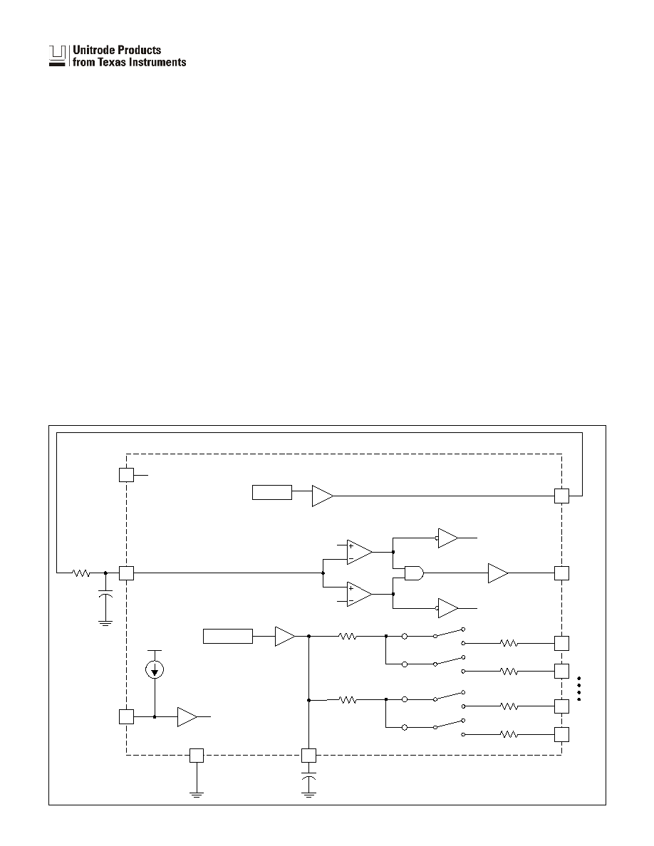
BLOCK DIAGRAM
UDG-98181
DESCRIPTION
The UCC5640 is an active terminator for Low Voltage Differential (LVD)
SCSI networks. This LVD only design allows the user to reach peak bus
performance while reducing system cost. The device is designed as an ac-
tive Y-terminator to improve the frequency response of the LVD Bus. De-
signed with a 1.5pF channel capacitance, the UCC5640 allows for minimal
bus loading for a maximum number of peripherals. With the UCC5640, the
designer will be able to comply with the Fast-40 SPI-2, Fast-80 SPI-3 and
Fast-160 SPI-4 specifications. The UCC5640 also provides a much-
needed system migration path for ever improving SCSI system standards.
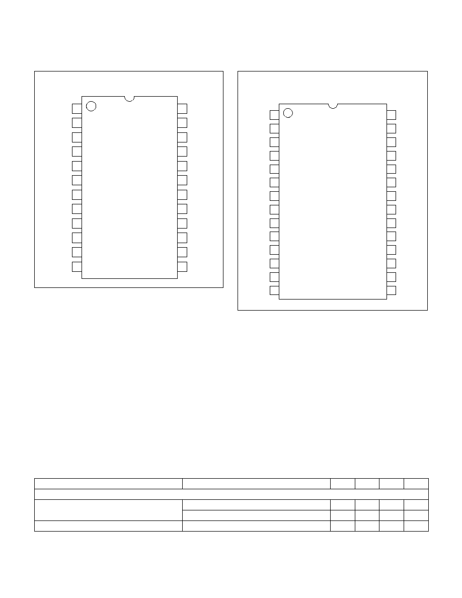
This device is available in the 24 pin TSSOP and 28 pin TSSOP for ease
of layout use.
The UCC5640 is not designed for use in single ended or high voltage dif-
ferential systems.
* 28 pin package only
2
UCC5640
ABSOLUTE MAXIMUM RATINGS
TERMPWR Voltage. . . . . . . . . . . . . . . . . . . . . . . . . . . . . . . +6V
Signal Line Voltage . . . . . . . . . . . . . . . . . . . . . . . . . . 0V to 3.6V
Package Dissipation . . . . . . . . . . . . . . . . . . . . . . . . . . . . . . . 1W
Storage Temperature . . . . . . . . . . . . . . . . . . . ≠65∞C to +150∞C
Junction Temperature . . . . . . . . . . . . . . . . . . . ≠55∞C to +150∞C
Lead Temperature (Soldering, 10 sec.) . . . . . . . . . . . . . +300∞C
Currents are positive into negative out of the specified terminal.
consult Packaging Section of Databook for thermal limitations
and considerations of package.
RECOMMENDED OPERATING CONDITIONS
TERMPWR Voltage . . . . . . . . . . . . . . . . . . . . . . . 2.7V to 5.25V
DIFFB
L6+
L8≠
L8+
L7≠
TRMPWR
L1+
L4≠
L3+
L4+
L1≠
L2+
L2≠
REG
L3≠
DIFSENS
L7+
L6≠
L5≠
12
11
10
9
8
7
6
5
4
3
2
1
13
14
15
16
17
18
19
20
21
22
23
24
L5+
L9≠
L9+
GND
DISCNCT
CONNECTION DIAGRAMS
TSSOP-24 (Top View)
PW24 Package
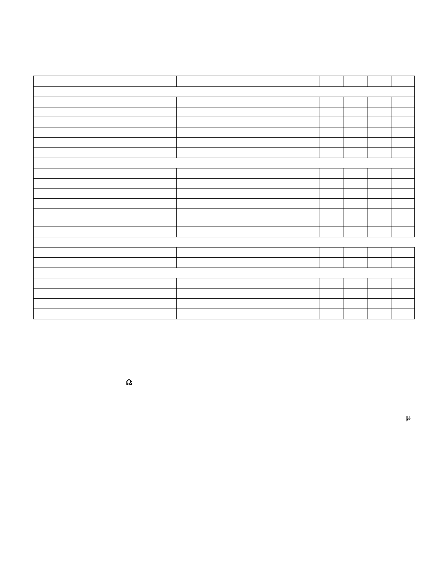
ELECTRICAL CHARACTERISTICS:
Unless otherwise stated, specifications apply for T
A
= 0∞C to 70∞C,
TRMPWR = 3.3V. T
A
= T
J
.
PARAMETER
TEST CONDITIONS
MIN
TYP
MAX
UNITS
TRMPWR Supply Current Section
TRMPWR Supply Current
No Load
25
mA
Disabled Terminator
400
µA
TRMPWR Voltage
2.7
5.25
V
DIFFB
L6+
L8≠
L8+
L7≠
TRMPWR
L1+
N/C
L4≠
L3+
L4+
L1≠
L2+
L2≠
REG
L3≠
DIFSENS
L7+
L6≠
L5≠
N/C
GND
14
13
12
11
10
9
8
7
6
5
4
3
2
1
15
16
17
18
19
20
21
22
23
24
25
26
27
28
L5+
N/C
DISCNCT
L9≠
L9+
LVD
TSSOP-28 (Top View)
PW28 Package
3
UCC5640
ELECTRICAL CHARACTERISTICS:
Unless otherwise stated, specifications apply for T
A
= 0∞C to 70∞C,
TRMPWR = 3.3V. T
A
= T
J
.
PARAMETER
TEST CONDITIONS
MIN
TYP
MAX
UNITS
Regulator Section
1.25V Regulator
DIFSENS connected to DIFFB
1.15
1.25
1.35
V
1.25V Regulator Source Current
DIFSENS connected to DIFFB
≠100
≠80
mA
1.25V Regulator Sink Current
DIFSENS connected to DIFFB
80
100
mA
1.3V Regulator
DIFFB connected to GND
1.2
1.3
1.4
V
1.3V Regulator Source Current
DIFSENS to GND
≠15
≠5
mA
1.3V Sink Current
DIFSENS to 3.3V
50
200
µA
Differential Termination Section
Differential Impedance
≠2.5mA to 4.5mA
100
105
110
Common Mode Impedance
L+ connected to L≠
110
150
165
Differential Bias Voltage
No load, L+ or L≠
100
125
mV
Common Mode Bias
1.15
1.25
1.35
V
Output Leakage, Disconnect
DISCNCT, TRMPWR = 0 to 5.25V,
V
LINE
= 0.2 to 5.25V
10
400
nA
Output Capacitance
Single ended measurement to ground (Note 1)
3
pF
Low Voltage Differential (LVD) Status Bit Section
I
SOURCE
V
LOAD
= 2.4V
≠6
≠4
mA
I
SINK
V
LOAD
= 0.4V
2
5
mA
Disconnect & Differential Sense Input Section
DISCNCT Threshold
0.8
2
V
Input Current
At 0V and 3.3V
≠30
≠10
µA
Differential Sense SE to LVD Threshold
0.5
0.7
V
Differential Sense LVD to HPD Threshold
1.9
2.4
V
Note 1: Guaranteed by design. Not 100% tested in production.
PIN DESCRIPTION
DIFFB: Differential sense filter pin should be connected
to a 4.7
µF capacitor and 50k resistor to Diff Sense.
DIFSENS: The SCSI bus differential sense line to detect
what type of devices are connected to the SCSI Bus.
DISCNCT: Disconnect pin shuts down the terminator
when it is not at the end of the bus.
GND: Ground.
L
n
≠: Negative line in differential applications for the
SCSI Bus.
L
n
+: Positive line for differential applications for the
SCSI Bus.
LVD: (28 pin package only) Indicates that the bus is in
LVD mode.
REG: Regulator bypass; must be connected to a 4.7 F
capacitor to ground.
TRMPWR: V
IN
2.7V to 5.25V power supply.

4
UCC5640
All SCSI buses require a termination network at each end to function properly. Specific termination requirements dif-
fer, depending on which types of SCSI driver devices are present on the bus. The UCC5640 is a low-voltage differen-
tial (LVD)-only device. It senses which types of drivers are present on the bus. If it detects the presence of a
single-ended (SE) or high-voltage differential (HVD) driver, the UCC5640 will place itself in a high-impedance input
state, effectively disconnecting the chip from the bus.
The UCC5640 senses what kinds of drivers are present on the bus by the voltage on SCSI bus control line
DIFFSENS, which is monitored by the DIFFB input pin. The DIFSENS output pin on the UCC5640 attempts to drive a
DIFFSENS control line to 1.3V. If only LVD devices are present, the DIFFSENS line will be successfully driven to that
voltage. If HVD drivers are present, they will pull the DIFFSENS line high. If any single-ended drivers are present, they
pull the DIFSENS line to ground (even if HVD drivers are also present on the bus). If the voltage on the DIFFB is be-
low 0.5V or above 2.4V, the UCC5640 enters the high-impedance SE/HVD state. If it is between 0.7V and 1.9V, the
UCC5640 enters the LVD mode. These thresholds accommodate differences in ground potential that can occur be-
tween the ends of long bus lines.
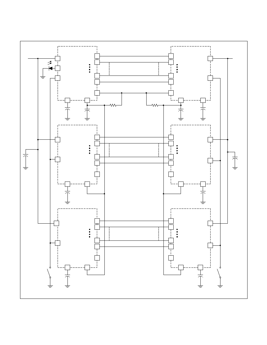
Three UCC5640 ICs are required at each end of the SCSI bus to terminate 27 lines (18 data, 9 control). Every
UCC5640 contains a DIFSENS driver, but only one should be used to drive the line at each end. The DIFSENS pin on
the other devices should be left unconnected.
On power up (the voltage on the TRMPWR pin rising above 2.7V), the UCC5640 assumes the SE/HVD mode.
The DIFFB inputs on all three chips at each end of the bus should be connected together. Properly filtered, noise on
DIFFB will not cause a false mode change. There should be a shared 50Hz noise filter implemented on DIFFB at
each end of the bus as close as possible to the DIFFB pins. This is implemented with a 50k
resistor between the
DIFFB and DIFSENS pins, and a 4.7 F capacitor from DIFFB to ground. See the Typical Application diagram at the
end of this datasheet.
In LVD mode, the regulated voltage is switched to 1.25V and a resistor network is presented to each line pair that pro-
vides common-mode impedance of 150
and differential impedance of 105 . The lines in each differential pair are bi-
ased so that when not driven, Line(n)+ and Line(n)- are driven 56mV below and above the common-mode bias
voltage (1.25V) respectively.
In SE/HVD mode, all the terminating resistors are switched off the bus. The 1.25V and 1.3V (DIFSENS) regulators are
left on.
When the disconnect input (DISCNCT) is active (high), the terminating resistors are switched off the bus and both
voltage regulators are turned off to save power. The mode change filter/delay function is still active and the LVD pin (in
the 28-pin package) continues to indicate the correct bus mode.
APPLICATION INFORMATION
5
UCC5640
The UCC5640 operates down to a TRMPWR voltage of 2.7V. This accommodates a 3.3V system with allowance for
supply tolerance (+10%), a unidirectional fusing device, and cable drop. The UCC3912 or UCC3918 is recommended
on a 3.3V systems and the UCC3916 is recommended on 5V systems in place of a fuse and diode implementation,
as its lower voltage drop provides additional voltage margin for the system.
Layout is important in all SCSI implementations and critical in SPI-3 and SPI-4 systems, which have stringent require-
ments on both the absolute value of capacitance on differential signal lines and the balancing of capacitance between
paired lines and from pair to pair.
Feedthroughs, through-hole connections, and etch lengths need to be carefully balanced. Standard multilayer power
and ground plane spacing adds about 1pF to each plane. Each feed-through will add 2.5pF to 3.5pF. Enlarging the
clearance holes on both power and ground planes reduces capacitance. Opening up the power and ground planes
under a through-hole connector reduces added capacitance in those applications. Capacitance is also affected by
components in close proximity on both sides of the board.
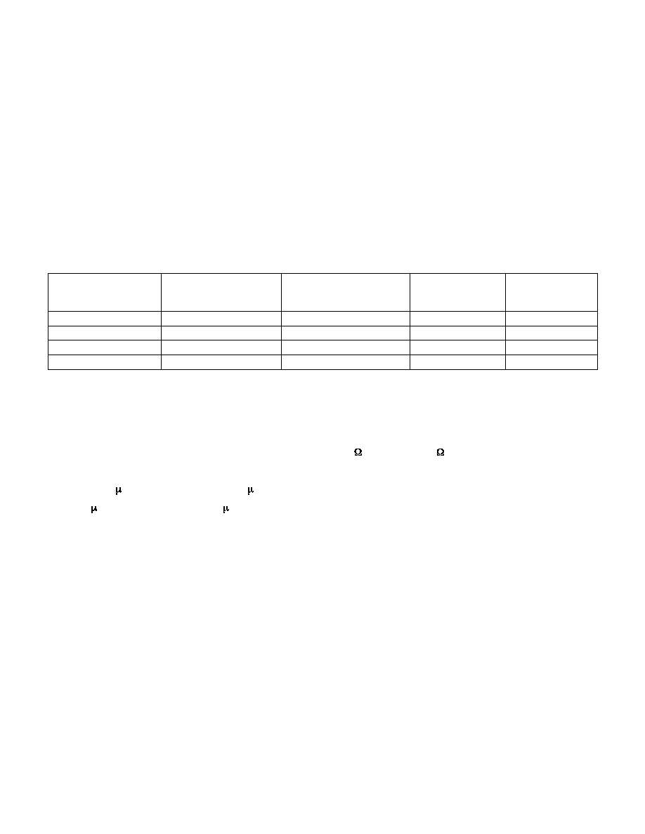
Maximum Capacitance
SCSI Class
Trace to GND:
REQ, ACK, DATA, Parity,
P_CRCA
Trace to Trace:
REQ, ACK, DATA, Parity,
P_CRCA
Trace to GND:
Other signals
Trace to Trace:
Other Signals
Ultra1
25 pF
N/A
25 pF
N/A
Ultra2
20 pF
10 pF
25 pF
13 pF
Ultra3/Ultra160
15 pF
8 pF
25 pF
13 pF
Ultra320
13 pF
6.5 pF
21 pF (est.)
10 pF (est.)
TI terminators are designed with very tightly controlled capacitance on their signal lines. Between the positive and
negative lines in a differential pair the difference is typically no more than 0.1pF, and only 0.3pF between pairs.
Multi-layer boards need to adhere to the 120W impedance standard, including the connector and feedthroughs. Bus
traces are normally run on the outer layers of the board with 4-mil etch and 4-mil spacing between the two lines in
each differential pair, and a minimum of 8-mil spacing to adjacent pairs to minimize crosstalk. Microstrip technology is
too low in impedance and should not be used-it is designed for 50
rather than 120
differential systems.
Decoupling capacitors should be installed as close as possible to the following input pins of the UCC5640:
TRMPWR: 4.7 F capacitor to ground, 0.01 F capacitor to ground (high-frequency, low ESR)
REG: 4.7 F capacitor to ground, 0.01 F capacitor to ground (high-frequency, low ESR)
APPLICATION INFORMATION
6
UCC5640
REG
TRMPWR
DISCNCT
TRMPWR
DIFFB
REG
Termpower
Termpower
28
15
12
1
11
11
1
24
DISCNCT 13
CONTROL LINES (9)
50k
50k
DIFF SENSE
3
2
4
3
4.7
µF
4.7
µF
25
22
26
23
L1+
L1≠
L9+
L9≠
L1+
L1≠
L9+
L9≠
4.7
µF
DIFFB
10
4.7
µF
REG
TRMPWR
DISCNCT
TRMPWR
DIFFB
REG
28
15
1
11
1
24
DISCNCT 13
DATA LINES (9)
3
2
4
3
4.7
µF
25
22
26
23
L1+
L1≠
L9+
L9≠
L1+
L1≠
L9+
L9≠
4.7
µF
DIFFB
10
REG
TRMPWR
DISCNCT
TRMPWR
DIFFB
REG
28
15
1
11
1
24
DISCNCT 13
DATA LINES (9)
3
2
4
3
4.7
µF
25
22
26
23
L1+
L1≠
L9+
L9≠
L1+
L1≠
L9+
L9≠
4.7
µF
DIFFB
10
4.7
µF
4.7
µF
UCC5640PW28
UCC5640PW24
UCC5640PW24
UCC5640PW28
UCC5640PW24
UCC5640PW28
27
LVD
S2*
S1*
* CLOSE S1 AND S2 TO CONNECT TERMINATORS
12
11
11
12
NC
NC
NC
NC
Figure 1. Application diagram.
APPLICATION INFORMATION
UDG-98180

IMPORTANT NOTICE
Texas Instruments Incorporated and its subsidiaries (TI) reserve the right to make corrections, modifications,
enhancements, improvements, and other changes to its products and services at any time and to discontinue
any product or service without notice. Customers should obtain the latest relevant information before placing
orders and should verify that such information is current and complete. All products are sold subject to TI's terms
and conditions of sale supplied at the time of order acknowledgment.
TI warrants performance of its hardware products to the specifications applicable at the time of sale in
accordance with TI's standard warranty. Testing and other quality control techniques are used to the extent TI
deems necessary to support this warranty. Except where mandated by government requirements, testing of all
parameters of each product is not necessarily performed.
TI assumes no liability for applications assistance or customer product design. Customers are responsible for
their products and applications using TI components. To minimize the risks associated with customer products
and applications, customers should provide adequate design and operating safeguards.
TI does not warrant or represent that any license, either express or implied, is granted under any TI patent right,
copyright, mask work right, or other TI intellectual property right relating to any combination, machine, or process
in which TI products or services are used. Information published by TI regarding third≠party products or services
does not constitute a license from TI to use such products or services or a warranty or endorsement thereof.
Use of such information may require a license from a third party under the patents or other intellectual property
of the third party, or a license from TI under the patents or other intellectual property of TI.
Reproduction of information in TI data books or data sheets is permissible only if reproduction is without
alteration and is accompanied by all associated warranties, conditions, limitations, and notices. Reproduction
of this information with alteration is an unfair and deceptive business practice. TI is not responsible or liable for
such altered documentation.
Resale of TI products or services with statements different from or beyond the parameters stated by TI for that
product or service voids all express and any implied warranties for the associated TI product or service and
is an unfair and deceptive business practice. TI is not responsible or liable for any such statements.
Mailing Address:
Texas Instruments
Post Office Box 655303
Dallas, Texas 75265
Copyright
2002, Texas Instruments Incorporated