UCC5641
SLUS397 - JANUARY 2000
FEATURES
∑ First LVD only Active Terminator
∑ Meets SCSI SPI-2 Ultra2 (Fast-40)
and Ultra3 / Ultra160 (Fast-80)
Standards
∑ 2.7V to 5.25V Operation
∑ Differential Failsafe Bias
∑ Reversed Disconnect Polarity
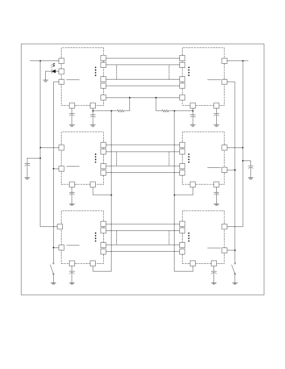
Low Voltage Differential (LVD) SCSI 9 Line Terminator
REF 1.25V
15
DISCNCT
27
LVD*
1
REG
11
DIFFB
4
L1≠
3
L1+
26
L9≠
25
L9+
56mV
SOURCE/SINK REGULATOR
REF 1.3V
1.3V
± 0.1V
0.7V > 0.5V
2.4V > 1.9V
HIGH IMPEDANCE RECEIVER
EVEN WITH POWER OFF
SINGLE
ENDED
HIGH POWER
DIFFERENTIAL
12
DIFSENS
SOURCE 5≠15mA
SINK 200
µA MAXIMUM (NOISE LOAD)
OPEN CIRCUIT ON POWER OFF
OR OPEN CIRCUIT IN A
DISABLED TERMINATOR MODE
10
µA
28
TRMPWR
LOW
FREQUENCY
FILTER
50Hz ≠ 60Hz
20k
124
124
52
52
52
52
4.7
µF
0.1
µF
14
GND
SOURCE ONLY FROM TRMPWR AND THE ENABLED TERMINATIONS
2.7V to 5.25V
56mV
+
≠
≠
+
56mV
+
≠
56mV
≠
+
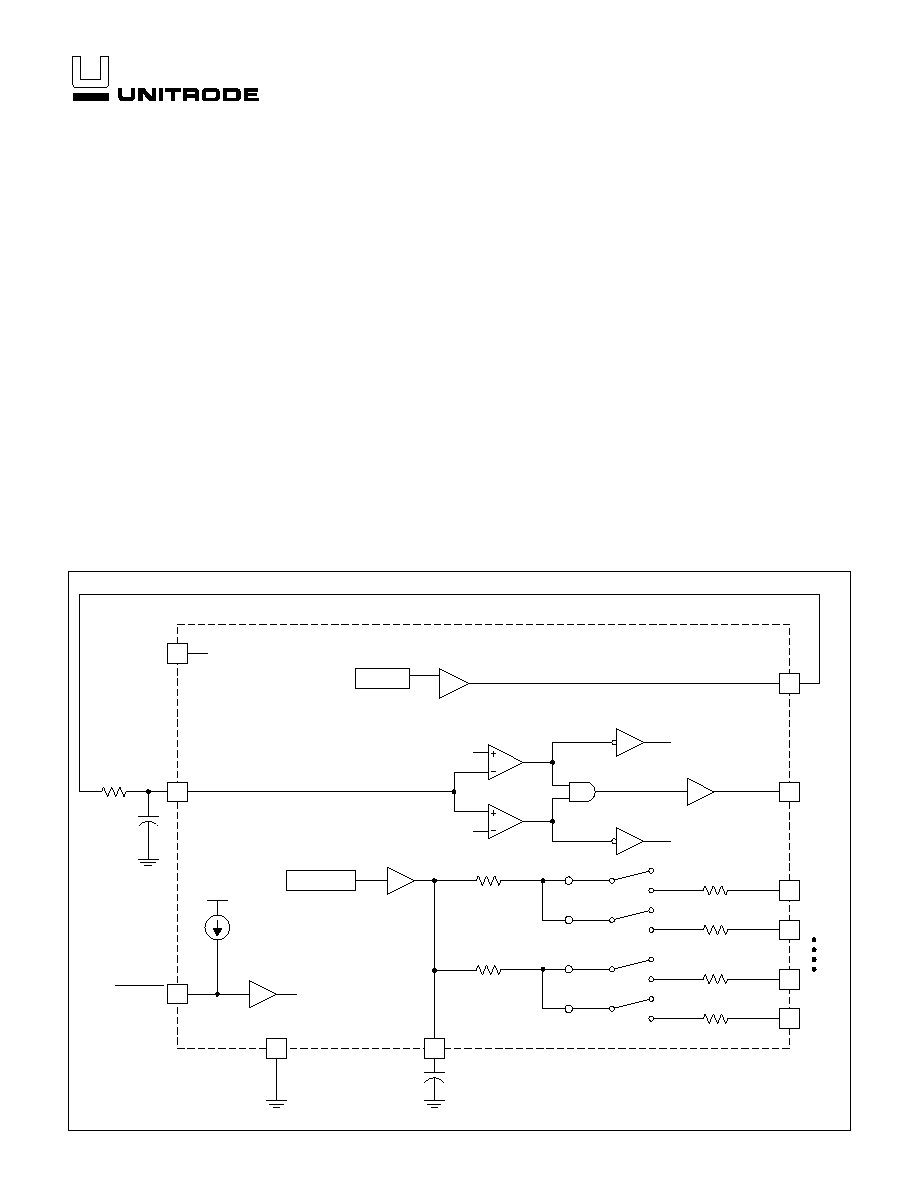
BLOCK DIAGRAM
UDG-99160
DESCRIPTION
The UCC5641 is an active terminator for Low Voltage Differential (LVD)
SCSI networks. This LVD only design allows the user to reach peak bus
performance while reducing system cost. The device is designed as an
active Y-terminator to improve the frequency response of the LVD Bus.
Designed with a 1.5pF channel capacitance, the UCC5641 allows for mini-
mal bus loading for a maximum number of peripherals. With the
UCC5641, the designer will be able to comply with the Fast-40 SPI-2 and
Fast-80 SPI-3 specifications. The UCC5641 also provides a much-needed
system migration path for ever improving SCSI system standards. This de-
vice is available in the 24 pin TSSOP and 28 pin TSSOP for ease of lay-
out use.
The UCC5641 is not designed for use in single ended or high voltage dif-
ferential systems.
* 28 pin package only
2
UCC5641
ABSOLUTE MAXIMUM RATINGS
TERMPWR Voltage. . . . . . . . . . . . . . . . . . . . . . . . . . . . . . . +6V
Signal Line Voltage . . . . . . . . . . . . . . . . . . . . . . . . . . 0V to 3.6V
Package Dissipation . . . . . . . . . . . . . . . . . . . . . . . . . . . . . . . 1W
Storage Temperature . . . . . . . . . . . . . . . . . . . ≠65∞C to +150∞C
Junction Temperature . . . . . . . . . . . . . . . . . . . ≠55∞C to +150∞C
Lead Temperature (Soldering, 10 sec.) . . . . . . . . . . . . . +300∞C
Currents are positive into negative out of the specified terminal.
consult Packaging Section of Databook for thermal limitations
and considerations of package.
RECOMMENDED OPERATING CONDITIONS
TERMPWR Voltage . . . . . . . . . . . . . . . . . . . . . . . 2.7V to 5.25V
DIFFB
L6+
L8≠
L8+
L7≠
TRMPWR
L1+
L4≠
L3+
L4+
L1≠
L2+
L2≠
REG
L3≠
DIFSENS
L7+
L6≠
L5≠
12
11
10
9
8
7
6
5
4
3
2
1
13
14
15
16
17
18
19
20
21
22
23
24
L5+
L9≠
L9+
GND
DISCNCT
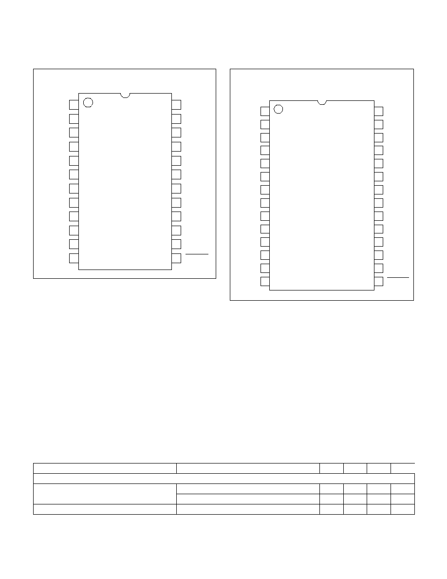
CONNECTION DIAGRAMS
TSSOP-24 (Top View)
PW24 Package
ELECTRICAL CHARACTERISTICS:
Unless otherwise stated, specifications apply for T
A
= 0∞C to 70∞C,
TRMPWR = 3.3V. T
A
= T
J
.
PARAMETER
TEST CONDITIONS
MIN
TYP
MAX
UNITS
TRMPWR Supply Current Section
TRMPWR Supply Current
No Load
25
mA
Disabled Terminator
400
µA
TRMPWR Voltage
2.7
5.25
V
DIFFB
L6+
L8≠
L8+
L7≠
TRMPWR
L1+
N/C
L4≠
L3+
L4+
L1≠
L2+
L2≠
REG
L3≠
DIFSENS
L7+
L6≠
L5≠
N/C
GND
14
13
12
11
10
9
8
7
6
5
4
3
2
1
15
16
17
18
19
20
21
22
23
24
25
26
27
28
L5+
N/C
DISCNCT
L9≠
L9+
LVD
TSSOP-28 (Top View)
PW28 Package

3
UCC5641
ELECTRICAL CHARACTERISTICS:
Unless otherwise stated, specifications apply for T
A
= 0∞C to 70∞C,
TRMPWR = 3.3V. T
A
= T
J
.
PARAMETER
TEST CONDITIONS
MIN
TYP
MAX
UNITS
Regulator Section
1.25V Regulator
DIFSENS connected to DIFFB
1.15
1.25
1.35
V
1.25V Regulator Source Current
DIFSENS connected to DIFFB
≠100
≠80
mA
1.25V Regulator Sink Current
DIFSENS connected to DIFFB
80
100
mA
1.3V Regulator
DIFFB connected to GND
1.2
1.3
1.4
V
1.3V Regulator Source Current
DIFSENS to GND
≠15
≠5
mA
1.3V Sink Current
DIFSENS to 3.3V
50
200
µA
Differential Termination Section
Differential Impedance
≠2.5mA to 4.5mA
100
105
110
Common Mode Impedance
L+ connected to L≠
110
150
165
Differential Bias Voltage
No load, L+ or L≠
100
125
mV
Common Mode Bias
1.15
1.25
1.35
V
Output Leakage, Disconnect
DISCNCT, TRMPWR = 0 to 5.25V,
V
LINE
= 0.2 to 5.25V
10
400
nA
Output Capacitance
Single ended measurement to ground (Note 1)
3
pF
Low Voltage Differential (LVD) Status Bit Section
I
SOURCE
V
LOAD
= 2.4V
≠6
≠4
mA
I
SINK
V
LOAD
= 0.4V
2
5
mA
Disconnect & Differential Sense Input Section
DISCNCT Threshold
0.8
2
V
Input Current
At 0V and 3.3V
≠30
≠10
µA
Differential Sense SE to LVD Threshold
0.5
0.7
V
Differential Sense LVD to HPD Threshold
1.9
2.4
V
Note 1: Guaranteed by design. Not 100% tested in production.
PIN DESCRIPTION
DIFFB: Differential sense filter pin should be connected
to a 0.1
µF capacitor and 20k resistor to Diff Sense.
DIFSENS: The SCSI bus differential sense line to detect
what type of devices are connected to the SCSI Bus.
DISCNCT: Disconnect pin shuts down the terminator
when it is not at the end of the bus.
GND: Ground.
L
n
≠: Negative line in differential applications for the
SCSI Bus.
L
n
+: Positive line for differential applications for the
SCSI Bus.
LVD: (28 pin package only) Indicates that the bus is in
LVD mode.
REG: Regulator bypass; must be connected to a 4.7 F
capacitor to ground.
TRMPWR: V
IN
2.7V to 5.25V supply.