UCC5642
LVD ONLY SCSI TERMINATOR
WITH REGULATOR AND SPI 3 DELAY
SLUS477 ≠ FEBRUARY 2000 ≠ REVISED DECEMBER 2000
1
POST OFFICE BOX 655303
∑
DALLAS, TEXAS 75265
D
LVD-Only Active Termination
D
2.7-V to 5.25-V Operation
D
Differential Failsafe Bias
D
Integrated SPI-3 Mode Change/Filter Delay
D
Thermal Packaging for Low Junction
Temperature and Better MTBF
D
2.85-V Regulator With Load Share
D
Meets Ultra2 (SPI-2 LVD), Ultra3/Ultra160
(SPI-3) and Ultra320 (SPI-4) Standards
description
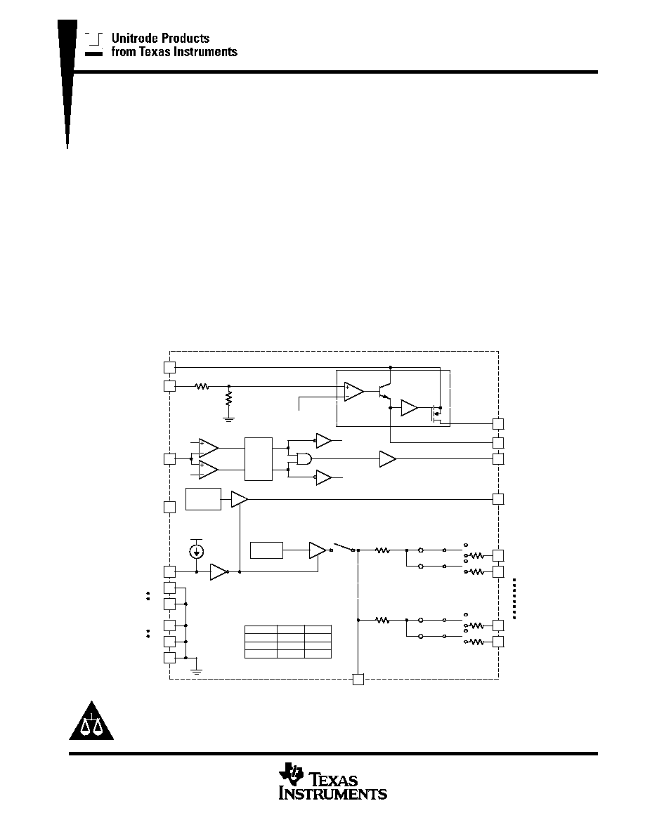
The UCC5642 is an LVD-only small computer system interface (SCSI) terminator that integrates the mode
change delay function required by the SPI-3 specification. The device senses what types of SCSI drivers are
present on the bus via the voltage on the DIFFSENS SCSI control line. Single-ended (SE) and high-voltage
differential (HVD) (EIA485) SCSI drivers are not supported. If the chip detects the presence of an SE or HVD
SCSI driver, it disconnects itself by switching all terminating resistors off the bus and enters a high-impedance
state. The terminator can also be commanded to disconnect the terminating resistors with the DISCNCT input.
Impedance is trimmed for accuracy and maximum effectiveness. Bus lines are biased to a failsafe state to
ensure signal integrity. A 2.85-V, 300-mA sourcing regulator on chip can share with two other UCC5642 devices
in a parallel configuration for a 900 mA total.
The UCC5642 is offered in a 36-pin QSOP (MWP) package for a temperature range of 0
∞
C to 70
∞
C.
block diagram
UDG-00158
11
6
DIFSENS
DIFFSENS
REF 1.3 V
ENABLE
21
L1≠
52
22
L1+
52
L9≠
L9+
56 mV
+ ≠
56 mV
-
+
124
34
52
33
52
56 mV
+ ≠
56 mV
≠ +
124
REG
5
DIFFB
0.6 V
2.1 V
FILTER/
DELAY
12
TRMPWR
LVD REF
1.25 V
SOURCE/SINK
REGULATOR
ENABLE
10
µ
A
28
26
HS/GND
HS/GND
32
GND
7
DISCNCT
SE
DISCNCT
HPD
LVD
DOWN
OPEN
DOWN
DOWN
DOWN
OPEN
OPEN
OPEN
MODE
SW1
OTHER
SWITCHES
HPD
LVD
SE
10
8
HS/GND
HS/GND
31
30
25
24
29
3.6 k
1.5 V
VOLTAGE
AMPLIFIER
CURRENT
AMPLIFIER
VCC TO 2.85 V REGULATOR
TTL DRIVERS
LVD
SHARE
VREG
VOUTM
VCC
4 k
SW1
Copyright
©
2000, Texas Instruments Incorporated
PRODUCTION DATA information is current as of publication date.
Products conform to specifications per the terms of Texas Instruments
standard warranty. Production processing does not necessarily include
testing of all parameters.
Please be aware that an important notice concerning availability, standard warranty, and use in critical applications of
Texas Instruments semiconductor products and disclaimers thereto appears at the end of this data sheet.
LINE3+
LINE8≠
TRMPWR
VREG
VCC
LINE2≠
LINE1+
LINE1≠
LINE2+
REG
GND
LINE3≠
LINE8+
LINE4+
LINE4≠
14
13
12
11
10
9
8
7
6
5
4
3
2
1
23
24
25
26
27
28
29
30
31
32
33
34
35
36
18
17
16
15
DIFFB
SHARE
DIFSENS
19
20
21
22
LINE5+
LINE5≠
DISCNCT
GND
LINE7≠
LINE7+
LINE6≠
LINE6+
VOUTM
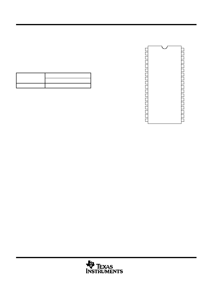
MWP PACKAGE
(TOP VIEW)
LINE9+
LINE9≠
GND
GND
GND
GND
SGND
LVD
N/C
UCC5642
LVD ONLY SCSI TERMINATOR
WITH REGULATOR AND SPI 3 DELAY
SLUS477 ≠ FEBRUARY 2000 ≠ REVISED DECEMBER 2000
2
POST OFFICE BOX 655303
∑
DALLAS, TEXAS 75265
package information
AVAILABLE OPTIONS
TJ
PACKAGED DEVICES
TJ
QSOP (MWP)
0
∞
C to 70
∞
C
UCC5642MWP
Available tape and reeled. Add R suffix to device type to
order quantities of 1000 devices per reel.
absolute maximum ratings over operating free-air temperature (unless otherwise noted)
TRMPWR voltage
6 V
. . . . . . . . . . . . . . . . . . . . . . . . . . . . . . . . . . . . . . . . . . . . . . . . . . . . . . . . . . . . . . . . . . . . . . . . . . .
Signal line voltage
0 V to 5 V
. . . . . . . . . . . . . . . . . . . . . . . . . . . . . . . . . . . . . . . . . . . . . . . . . . . . . . . . . . . . . . . . . . . .
Storage temperature, T
stg
≠65
∞
C to 150
∞
C
. . . . . . . . . . . . . . . . . . . . . . . . . . . . . . . . . . . . . . . . . . . . . . . . . . . . . . . . .
Junction temperature, T
J
≠55
∞
C to 150
∞
C
. . . . . . . . . . . . . . . . . . . . . . . . . . . . . . . . . . . . . . . . . . . . . . . . . . . . . . . . . .
Lead temperature (soldering, 10 sec.)
300
∞
C
. . . . . . . . . . . . . . . . . . . . . . . . . . . . . . . . . . . . . . . . . . . . . . . . . . . . . .
Stresses beyond those listed under "absolute maximum ratings" may cause permanent damage to the device. These are stress ratings only, and
functional operation of the device at these or any other conditions beyond those indicated under "recommended operating conditions" is not
implied. Exposure to absolute-maximum-rated conditions for extended periods may affect device reliability.
All voltages are with respect to GND. Currents are positive into, negative out of the specified terminal. Consult Packaging Section of the Interface
Products Data Book (TI Literature Number SLUD002) for thermal limitations and considerations of packages.
recommended operating conditions
TRMPWR voltage
2.7 V to 5.25 V
. . . . . . . . . . . . . . . . . . . . . . . . . . . . . . . . . . . . . . . . . . . . . . . . . . . . . . . . . . . . . . . . .
UCC5642
LVD ONLY SCSI TERMINATOR
WITH REGULATOR AND SPI 3 DELAY
SLUS477 ≠ FEBRUARY 2000 ≠ REVISED DECEMBER 2000
3
POST OFFICE BOX 655303
∑
DALLAS, TEXAS 75265
electrical characteristics, these specifications apply for T
A
= T
J
= 0
∞
C to 70
∞
C, TRMPWR = 2.7 V to
5.25 V, VCC = 4.75 V to 5.25 V,(unless otherwise stated)
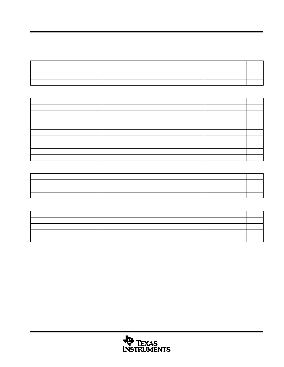
TRMPWR supply current section
PARAMETER
TEST CONDITIONS
MIN
TYP
MAX
UNITS
TRMPWR supply current
LVD SCSI mode
25
40
mA
TRMPWR supply current
DISCNCT mode
0.5
1
mA
VCC supply current
5
10
mA
regulator section
PARAMETER
TEST CONDITIONS
MIN
TYP
MAX
UNITS
1.25 V regulator output voltage
0.5
VCM
2,
See Note 1
1.15
1.25
1.35
V
1.25 V regulator source current
VREG = 0 V
≠100
≠80
mA
1.25 V regulator sink current
VREG = 3.0 V
80
100
mA
2.85 V regulator output voltage
2.79
2.85
2.91
V
2.85 V regulator source current
≠800
≠600
≠400
mA
2.85 V regulator sink current
3
5
8
mA
Share output gain
4.8
6.2
7.2
V/A
Share input gain
0.130
0.160
0.192
A/V
VOUTM input resistance
4
7.6
12
k
diff sense driver (DIFFSENS) section
PARAMETER
TEST CONDITIONS
MIN
TYP
MAX
UNITS
1.3 V DIFFSENS output voltage
0.5 mA
IDIFSENS
50
µ
A
1.2
1.3
1.4
V
1.3 V DIFFSENS source current
VDIFFSENS = 0 V
≠15
≠5
mA
1.3 V DIFFSENS sink current
VDIFFSENS = 2.75 V
50
200
µ
A
differential termination section
PARAMETER
TEST CONDITIONS
MIN
TYP
MAX
UNITS
Differential impedance
100
105
110
Common mode impedance
L+ and L≠ shorted together,
See Note 2
110
140
165
Differential bias voltage
100
125
mV
Common mode bias
L+ and L≠ shorted together
1.15
1.25
1.35
V
NOTES:
1. VCM is applied to all L+ and L≠ lines simultaneously.
2.
Z
CM
+
(2.0 V
*
0.5 V)
I
I
VCM(max)
*
I
VCM(min)
@ VCM(max) = 2.0, VCM(min) = 0.5 V.
3. Ensured by design. Not production tested.
UCC5642
LVD ONLY SCSI TERMINATOR
WITH REGULATOR AND SPI 3 DELAY
SLUS477 ≠ FEBRUARY 2000 ≠ REVISED DECEMBER 2000
4
POST OFFICE BOX 655303
∑
DALLAS, TEXAS 75265
electrical characteristics, these specifications apply for T
A
= T
J
= 0
∞
C to 70
∞
C, TRMPWR = 2.7 V to
5.25 V, VCC = 4.75 V to 5.25 V, (unless otherwise stated)
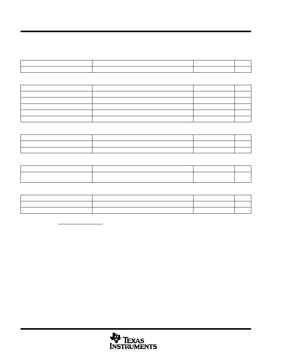
disconnected termination section (applies to each line pair, 1≠9, in DISCNCT, SE or HVD mode)
Output leakage
400
nA
Output capacitance
Single ended measurement to ground,
See Note 3
3
pF
disconnect (DISCNCT) and diff buffer (DIFFB) input section
PARAMETER
TEST CONDITIONS
MIN
TYP
MAX
UNITS
DISCNCT threshold
0.8
2.0
V
DISCNCT input current
≠30
≠10
µ
A
DIFFB SE to LVD SCSI threshold
0.5
0.7
V
DIFFB LVD SCSI to HPD threshold
1.9
2.4
V
DIFFB input current
≠1
1
µ
A
low voltage differential (LVD) status bit section
PARAMETER
TEST CONDITIONS
MIN
TYP
MAX
UNITS
ISOURCE
VLOAD = 2.4 V
≠6
≠4
mA
ISINK
VLOAD = 0.4 V
2
5
mA
time delay/filter section
PARAMETER
TEST CONDITIONS
MIN
TYP
MAX
UNITS
Mode change delay
A new mode change can start any time after a previous
mode change has been detected.
100
190
300
ms
thermal shutdown section
PARAMETER
TEST CONDITIONS
MIN
TYP
MAX
UNITS
Thermal shutdown threshold
For increasing temperature,
See Note 3
140
155
170
∞
C
Thermal shutdown hysteresis
10
∞
C
NOTES:
1. VCM is applied to all L+ and L≠ lines simultaneously.
2.
Z
CM
+
(2.0 V
*
0.5 V)
I
I
VCM(max)
*
I
VCM(min)
@ VCM(max) = 2.0, VCM(min) = 0.5 V.
3. Ensured by design. Not production tested.

UCC5642
LVD ONLY SCSI TERMINATOR
WITH REGULATOR AND SPI 3 DELAY
SLUS477 ≠ FEBRUARY 2000 ≠ REVISED DECEMBER 2000
5
POST OFFICE BOX 655303
∑
DALLAS, TEXAS 75265
pin descriptions
DIFFB: Input pin for the comparators that select SE, LVD or HIPD modes of operation. This pin should be
decoupled with a 0.1-
µ
F capacitor to ground and then coupled to the DIFSENS pin through a 20-k
resistor.
DIFSENS: SCSI bus DIFFSENS line driver.
DISCNCT: Input pin used to shut down the terminator if the terminator is not connected at the end of the bus.
Connect this pin to ground to activate the terminator or open to disable the terminator.
HS/GND: Heat sink ground pins. Connected to large ground area PC board traces to increase the power
dissipation capability.
GND: Power supply return.
L1≠ thru L9≠: Line termination pins. Negative lines in differential pair. In HIPD and SE mode, these lines are
high impedance.
L1+ thru L9+: Line termination pins. Positive lines in differential pair. In HIPD and SE mode, these lines are high
impedance.
REG: Regulator bypass pin, must be connected to a 4.7-
µ
F capacitor to ground and a high frequency, low ESR
0.01-
µ
F capacitor to ground.
SHARE: Load share pin for the 2.85-V regulator. Connect to the SHARE pins of the other devices in a parallel
configuration.
TRMPWR: 2.7-V to 5.25-V power input pin. Bypass near the terminators with a 4.7-
µ
F capacitor and a high
frequency, low ESR 0.01-
µ
F capacitor to ground.
VCC: 4.75-V to 5.25-V power-input pin. Connect to a 4.7-
µ
F capacitor and a low ESR 0.01-
µ
F capacitor to
ground.
VOUTM: V
REG
voltage feedback input pin for the 2.85-V regulator.
VREG: 2.85-V regulator output pin, must be connected to a 10-
µ
F low ESR capacitor.
APPLICATION INFORMATION
All SCSI buses require a termination network at each end to function properly. Specific termination requirements
differ, depending on which types of SCSI driver devices are present on the bus. The UCC5642 is a low-voltage
differential (LVD) only device. It senses which types of drivers are present on the bus. If it detects the presence
of a single-ended (SE) or high-voltage differential (HVD) driver, the UCC5642 will place itself in a
high-impedance input state, effectively disconnecting the chip from the bus.
The UCC5642 senses what kinds of drivers are present on the bus by the voltage on SCSI bus control line
DIFFSENS, which is monitored by the DIFFB input pin. The DIFSENS output pin on the UCC5642 attempts to
drive a DIFFSENS control line to 1.3 V. If only LVD devices are present, the DIFFSENS line will be successfully
driven to that voltage. If HVD drivers are present, they will pull the DIFFSENS line high. If any single-ended
drivers are present, they pull the DIFSENS line to ground (even if HVD drivers are also present on the bus). If
the voltage on the DIFFB is below 0.5 V or above 2.4 V, the UCC5642 enters the high-impedance SE/HVD state.
If it is between 0.7 V and 1.9 V, the UCC5642 enters the LVD mode. These thresholds accommodate differences
in ground potential that can occur between the ends of long bus lines.

UCC5642
LVD ONLY SCSI TERMINATOR
WITH REGULATOR AND SPI 3 DELAY
SLUS477 ≠ FEBRUARY 2000 ≠ REVISED DECEMBER 2000
6
POST OFFICE BOX 655303
∑
DALLAS, TEXAS 75265
APPLICATION INFORMATION
Three UCC5642 ICs are required at each end of the SCSI bus to terminate 27 lines (18 data, 9 control). Every
UCC5642 contains a DIFSENS driver, but only one should be used to drive the line at each end. The DIFSENS
pin on the other devices should be left unconnected.
On power up (the voltage on the TRMPWR pin rising above 2.7 V), the UCC5642 assumes the SE/HVD mode.
If the voltage on the DIFFB input indicates LVD mode, the chip waits 100 ms to 300 ms before changing the
mode of the bus. If the voltage at the DIFFB input later crosses one of the thresholds, the UCC5642 again waits
100 ms to 300 ms before changing the mode of the bus. The magnitude of the delay is the same when changing
in or out of either bus mode. A new mode change can start anytime after a previous mode change has been
detected.
The DIFFB inputs on all three chips at each end of the bus should be connected together. Properly filtered, noise
on DIFFB will not cause a false mode change. There should be a shared 50-Hz noise filter implemented on
DIFFB at each end of the bus as close as possible to the DIFFB pins. This is implemented with a 20-k
resistor
between the DIFFB and DIFSENS pins, and a 0.1-
µ
F capacitor from DIFFB to ground. See the
Typical
Application diagram at the end of this data sheet.
The 5-V to 2.85-V regulator in the UCC5642 can run as a stand-alone regulator by connecting the output
(VREG) to the voltage-feedback input (VOUTM). Also connect to VREG a low ESR 10-
µ
F capacitor. The other
side of the low ESR capacitor is connected to GND. When the load sinks current from VREG the voltage will
start to drop, this drop will be detected by the feedback at VOUTM, and more current will be driven by VREG.
Because the feedback loop has a slight delay the 10-
µ
F low ESR capacitor is very important to supply current
for fast transient and to stabilize the loop. In this configuration VREG can supply about 300-mA.
To supply more current, all three VREG output can be connected together. To keep one regulator from supplying
all the current the SHARE pins need to be connected together. Because this is an unusual feature a short
description follows.
In the stand alone configuration, the SHARE pin voltage is proprotional to the output current. By design, the
SHARE pin drive is a strong pullup and a weak pulldown. When the share pin is pulled up from outside the
UCC5642 the current out of VREG is proportional to the voltage on the SHARE pin.
In the parallel configuration, the VREG pins are connected together to provided the load current. The SHARE
pins are connected together so the regulators will share the load current. When the load is appllied, one
regulator will start to supply more current than the other two and will drive the common SHARE connection
higher. This higher voltage on the common SHARE connection will cause each of the other two regulators to
supply the same current, thus sharing the load current. In this configuration one regulator sets the voltage and
supplies one-third of the load current. Each of the other regulators supply an additional one-third of the current.
Because the 10
µ
F stabilizes the voltage feedback loop, there must be one 10-
µ
F low ESR capacitor near each
V
REG
output for each UCC5642. If better transient response is required there can be as much as 100
µ
F for
each UCC5642.

UCC5642
LVD ONLY SCSI TERMINATOR
WITH REGULATOR AND SPI 3 DELAY
SLUS477 ≠ FEBRUARY 2000 ≠ REVISED DECEMBER 2000
7
POST OFFICE BOX 655303
∑
DALLAS, TEXAS 75265
APPLICATION INFORMATION
REG
TRMPWR
VREG
VCC
DIFFB
SHARE
Termpower
Termpower
12
25
6
11
5
6
VOUTM
CONTROL LINES (9)
20 k
20 k
DIFF SENSE
22
22
21
21
4.7
µ
F
0.1
µ
F
33
33
34
34
L1+
L1≠
L9+
L9≠
L1+
L1≠
L9+
L9≠
UCC5642
UCC5642
24 VCC
VREG
7
29
30
VOUTM
SHARE
DISCNCT
4.7
µ
F
10
µ
F
4.7
µ
F
4.7
µ
F
10
µ
F
4.7
µ
F
12
25
24
29
30
REG
DIFFB
11
5
4.7
µ
F
0.1
µ
F
7
DISCNCT
TRMPWR
REG
TRMPWR
VREG
DIFFB
12
25
11
5
DATA LOW BYTE LINES (9)
22
22
21
21
4.7
µ
F
33
33
34
34
L1+
L1≠
L9+
L9≠
L1+
L1≠
L9+
L9≠
UCC5642
UCC5642
24 VCC
7
29
30
VOUTM
SHARE
DISCNCT
10
µ
F
4.7
µ
F
10
µ
F
4.7
µ
F
12
25
24
29
30
REG
DIFFB
11
5
4.7
µ
F
7
DISCNCT
TRMPWR
REG
TRMPWR
VREG
VCC
DIFFB
SHARE
12
25
11
5
VOUTM
DATA HIGH BYTE LINES (9)
22
22
21
21
4.7
µ
F
33
33
34
34
L1+
L1≠
L9+
L9≠
L1+
L1≠
L9+
L9≠
UCC5642
UCC5642
24 VCC
VREG
7
29
30
VOUTM
SHARE
DISCNCT
10
µ
F
4.7
µ
F
10
µ
F
4.7
µ
F
12
25
24
29
30
REG
DIFFB
11
5
4.7
µ
F
7
DISCNCT
TRMPWR
VCC
VREG
2.85 V Load
VCC
VREG
2.85 V Load
0.01
µ
F
0.01
µ
F
0.01
µ
F
0.01
µ
F
0.01
µ
F
0.01
µ
F
0.01
µ
F
0.01
µ
F
VCC
SHARE
VOUTM
VREG
0.01
µ
F
0.01
µ
F
0.01
µ
F
0.01
µ
F
0.01
µ
F
0.01
µ
F
Figure 1. Application Diagram

IMPORTANT NOTICE
Texas Instruments and its subsidiaries (TI) reserve the right to make changes to their products or to discontinue
any product or service without notice, and advise customers to obtain the latest version of relevant information
to verify, before placing orders, that information being relied on is current and complete. All products are sold
subject to the terms and conditions of sale supplied at the time of order acknowledgment, including those
pertaining to warranty, patent infringement, and limitation of liability.
TI warrants performance of its semiconductor products to the specifications applicable at the time of sale in
accordance with TI's standard warranty. Testing and other quality control techniques are utilized to the extent
TI deems necessary to support this warranty. Specific testing of all parameters of each device is not necessarily
performed, except those mandated by government requirements.
Customers are responsible for their applications using TI components.
In order to minimize risks associated with the customer's applications, adequate design and operating
safeguards must be provided by the customer to minimize inherent or procedural hazards.
TI assumes no liability for applications assistance or customer product design. TI does not warrant or represent
that any license, either express or implied, is granted under any patent right, copyright, mask work right, or other
intellectual property right of TI covering or relating to any combination, machine, or process in which such
semiconductor products or services might be or are used. TI's publication of information regarding any third
party's products or services does not constitute TI's approval, warranty or endorsement thereof.
Mailing Address:
Texas Instruments
Post Office Box 655303
Dallas, Texas 75265
Copyright
©
2001, Texas Instruments Incorporated